Broad-spectrum light emission at microscopic breakdown sites in
metal-insulator-silicon tunnel diodes
J. G. Mihaychuk, M. W. Denhoff, S. P. McAlister, W. R. McKinnon, and A. Chin
Citation: Journal of Applied Physics 98, 054502 (2005); doi: 10.1063/1.2031946 View online: http://dx.doi.org/10.1063/1.2031946
View Table of Contents: http://scitation.aip.org/content/aip/journal/jap/98/5?ver=pdfcov Published by the AIP Publishing
Articles you may be interested in
Infrared emission from Ge metal-insulator-semiconductor tunneling diodes Appl. Phys. Lett. 89, 261913 (2006); 10.1063/1.2420783
Carrier lifetime measurement on electroluminescent metal–oxide–silicon tunneling diodes Appl. Phys. Lett. 79, 2264 (2001); 10.1063/1.1405429
Enhanced reliability of electroluminescence from metal–oxide–silicon tunneling diodes by deuterium incorporation
Appl. Phys. Lett. 78, 1397 (2001); 10.1063/1.1353817
Hot carrier recombination model of visible electroluminescence from metal–oxide–silicon tunneling diodes Appl. Phys. Lett. 77, 4347 (2000); 10.1063/1.1332825
Hot electron impact excitation cross-section of Er 3+ and electroluminescence from erbium-implanted silicon metal-oxide-semiconductor tunnel diodes
Appl. Phys. Lett. 71, 2824 (1997); 10.1063/1.120147
Broad-spectrum light emission at microscopic breakdown sites
in metal-insulator-silicon tunnel diodes
J. G. Mihaychuk, M. W. Denhoff, S. P. McAlister,a兲 and W. R. McKinnon
National Research Council, Institute for Microstructural Sciences, Building M-50, Montreal Road, Ottawa, ON K1A 0R6, Canada
A. Chin
Department of Electronics Engineering, National Chiao Tung University, Hsinchu 300, Taiwan 共Received 14 January 2005; accepted 18 July 2005; published online 6 September 2005兲
In addition to Si band-edge electroluminescence共EL兲 near 1.1 eV, we observe hot-electron EL in metal-insulator-silicon tunnel diodes that can span a detector-limited range from 0.7 to 2.6 eV 共1780–480 nm兲. The maximum photon energy increases with increasing forward bias. In one implementation, sub-micron-sized EL sites appear during the forward-bias stress. The number of sites grows linearly with the current, consistent with the dielectric breakdown of the insulator. We compare the poststress current-voltage data with the quantum-point-contact model. Results are presented for various p-type Si共100兲 devices having 2–8-nm-thick SiO2, Al2O3, and HfOxNy
insulators. We also describe devices in which electron-beam lithography of an 18-nm-thick SiO2is used to define EL sites. © 2005 American Institute of Physics.关DOI:10.1063/1.2031946兴
I. INTRODUCTION
Silicon is a favored material for photonics as well as microelectronics due to its low cost, established process technology, and high material quality. However, crystalline Si is a very poor light emitter, in which nonradiative recom-bination exceeds phonon-assisted radiative recomrecom-bination because the band-gap is indirect. Nevertheless, the work on Si light-emitting devices1–3has intensified in the past decade. Increasingly this research addresses eventual performance limitations of integrated circuits.4,5A delay in the intercon-nects will impair signaling across integrated circuits. While optical interconnects might offer a solution,6a Si-compatible light source is desirable.
Many electrically driven Si light emitters have used ma-terials such as porous Si,7 Si-rich oxides,8,9 Si nanocrystals,10,11 or rare-earth dopants.12–15 Another approach16,17 employed a light-recycling top surface. Re-cently, stimulated emission was demonstrated18 in a ridge
pn diode fabricated using spin-on B dopant and SiO2
nanoparticles.
Electroluminescence共EL兲 has also been achieved in pla-nar Si microelectronics using, for example, dislocation loops formed by B implantation19or avalanching pn junctions.20–22 EL imaging has been used to analyze Si device operation23 and reliability.24,25Many light emitters have also been imple-mented as metal-insulator-silicon 共MIS兲 tunnel diodes.26–37 Recently, Rasras et al. outlined the connection between the substrate current and the EL at insulator breakdown sites.38
In this work we study MIS devices with SiO2, Al2O3, and HfOxNyinsulators. We examine visible and infrared EL,
including pointlike emission associated with the dielectric breakdown of the insulator. We also demonstrate devices in
which conduction and EL occur at locations defined by the electron-beam lithography of a thick SiO2 layer.
This article is organized as follows. In Sec. II we discuss the mechanisms for both the band-gap and the broad-spectrum EL. Section III outlines a model for postbreakdown current-voltage 共I-V兲 characteristics. In Sec. IV we describe the device structures and measurement methods. Section V reports measurement results for several device compositions. We present a detailed discussion of our findings in Sec. VI and more general conclusions in Sec. VII.
II. EL MECHANISMS A. Band-gap EL
As depicted in Fig. 1 by the transition labeled “1”, Si has an indirect band gap with the conduction-band 共CB兲 mini-mum near the Brillouin zone edge along the ⌫-X or 关100兴 axis and the valence-band共VB兲 maxima at the zone center ⌫. The radiative recombination of an electron-hole pair requires a third quantum to conserve momentum, normally a phonon. For this reason the nonradiative recombination involving in-terface states, impurities, and Auger processes dominates. Furthermore, the free-carrier optical absorption in Si can re-duce light transmission. Nevertheless, EL in Si occurs with quantum efficiency⬃10−6and is readily observed using sen-sitive detectors. The band-gap EL spectra from MIS tunnel diodes have been modeled considering the relevant phonon energies and the contributions of continuum and bound excitons.35
B. Broad-spectrum EL 1. Hot-carrier transitions
For MIS devices on p-type Si in forward bias, electrons are transported across the insulator to the Si substrate. We therefore consider only the transitions by an electron in a CB, as shown in Fig. 1. However, in addition to CB-VB
a兲Author to whom correspondence should be addressed; electronic mail: [email protected]
0021-8979/2005/98共5兲/054502/9/$22.50 98, 054502-1 © 2005 American Institute of Physics [This article is copyrighted as indicated in the article. Reuse of AIP content is subject to the terms at: http://scitation.aip.org/termsconditions. Downloaded to ] IP:
transitions共electron-hole recombination兲, we include CB-CB transitions by energetic electrons. A radiative CB-CB transi-tion may occur in the first CB or between two CB’s and can be understood as the inverse process to the free-carrier ab-sorption of photons.
Several workers have modeled39–41 EL in Si based on transitions of energetic carriers between multiple bands. Both direct and phonon-assisted transitions were considered for CB-VB, CB-CB, and VB-VB cases. The spectra depended strongly on the carrier energy distribution function. Pavesi et al. illustrated this for phonon-assisted CB-CB transitions us-ing thermal共Maxwellian兲 and “box” distributions of injected electrons 共see Fig. 8 of Ref. 39兲. For a thermal distribution with carrier temperature 1700 K, the EL intensity decreased exponentially with increasing photon energy. In contrast a box distribution centered at 4.0 eV with a width of 0.5 eV yielded a slowly varying spectrum from 1.0 to 3.5 eV, with a weaker tail from 3.5 to 4.5 eV and a very abrupt cutoff above 4.5 eV.
Models that use a single steady-state distribution func-tion may be appropriate in some devices. In our devices, however, electrons first enter a hole accumulation layer but may encounter a region of low-field and uniform hole con-centrations deeper in the substrate. Thus, electron energy dis-tributions could range from a narrow distribution of tunnel-ing electrons to a thermal distribution in equilibrium with the Si lattice.
Femtosecond-time-resolved photoemission studies42 in unbiased, atomically clean bulk Si共100兲 suggest this level of complexity, even in the absence of carrier heating due to an applied electric field. Through electron-electron and electron-phonon scattering electrons rapidly assume a ther-mal distribution with a temperature much higher than that of the crystal lattice. Through a succession of electron-phonon scattering events, these hot electrons relax to energies near
the bottom of the X valley within 1 ps and recombine with holes over much longer time scales. Since both hot and equi-librium electrons may be present simultaneously in MIS tun-nel diodes, the EL spectrum will generally include contribu-tions of multiple distribution funccontribu-tions.
2. Above- and below-gap EL
Many studies concerning Si devices address either the visible or the near-IR EL, often due to the spectral range of detectors. We will consider both parts of the spectrum.
Regarding the above-gap EL, several reports address MIS tunnel diodes.26–34The model spectra39suggest that the above-gap EL results from CB-CB transitions of electrons that have not cooled significantly. The CB-VB transitions can contribute similarly41 where the hole density is above 1019cm−3. The EL spectrum is expected to shift to shorter wavelengths with increasing forward bias. An alternative proposal26 stated that the above-gap EL was due to the re-combination of hot electrons and holes generated via impact ionization and described by Wolff distributions, given that the observed spectrum did not shift with bias.
Turning to the below-gap EL, one might invoke transi-tions via defect states within the Si band-gap. However, it is not clear that the spectrum due to defects would span the wide range of photon energies to be considered here. Alter-natively, the below-gap EL is compatible with models39 for the CB-CB EL. Although details depend on the distribution function considered, the intensity of the CB-CB EL between 0.5 and 1 eV can be similar to that of the CB-VB EL.
Finally, we note that the above-gap EL tends to originate in a relatively shallow layer of the Si substrate, while the below-gap EL is free of this restriction. While Si is transpar-ent for photon energies below the band gap, optical absorp-tion becomes increasingly strong as the photon energy in-creases to above 1.1 eV. For example, while light at 1.55 eV 共wavelength =800 nm兲 can originate within a depth ␦
= 10m, at 3.10 eV共=400 nm兲 one finds that␦= 0.1m, where 1 /␦is the optical absorption coefficient.43
III. CURRENT-VOLTAGE MODEL
In MIS tunnel diodes the physical alteration of the di-electric during a breakdown event should occur preferen-tially at locations that coincide with thin spots where the electric field is greatest. In addition, the current due to tun-neling grows exponentially for a linear decrease in the bar-rier width. The structure, composition, and electrode-edge effects may also influence the formation of breakdown sites. In a thorough review of the field, Miranda and Suñé compared44 several models for the current 共or conductance兲 as a function of voltage following dielectric breakdown in MIS structures with ultrathin insulators. The authors identi-fied several different categories of conduction according to the leakage current level or the current noise/instability: Fowler-Nordheim tunneling, stress-induced leakage current, soft breakdown, hard breakdown, and nonlinear hard break-down. The quantum-point-contact 共QPC兲 model was found to provide a relatively simple expression for fitting the I-V characteristics following either a soft or a hard breakdown.
FIG. 1. Si band structure and EL processes.共1兲 Phonon-assisted 共⌬k⫽0兲 recombination near the 1.1-eV band gap.共2兲 Direct 共⌬k=0兲 recombination of a hot electron.共3兲 Direct and 共4兲 phonon-assisted hot-electron CB-CB transitions.
054502-2 Mihaychuk et al. J. Appl. Phys. 98, 054502共2005兲
The QPC model serves as a useful reference point for any discussion of postbreakdown I-V characteristics in MIS devices.
The QPC model omits direct tunneling and considers nanometer-scale conductive damage channels through a ⬃5-nm-thick insulator. The lateral confinement leads to the quantization of the transverse momentum for electrons tun-neling through these constrictions. The separation between the associated energy subbands is in inverse proportion to the area of the constriction. Conduction occurs by ballistic tun-neling transport through a potential barrier of height ⌽. In the zero-temperature limit, the total current I through N simi-lar breakdown sites is
I =
冉
2e 2 h冊
N再
Vc+ 1 ␣ln冋
1 + exp兵␣关⌽ −Vc兴其 1 + exp兵␣关⌽ + 共1 −兲Vc兴其册
冎
, 共1兲 where the potential drop across the constriction is Vc. Thequantity ␣ parametrizes the shape of a parabolic potential barrier. The value 0⬍⬍1 represents the fraction of the potential dissipated on the source side of the constriction. The factor 2e2/ h is the quantum conductance unit.
The potential drop across the constriction is
Vc= V − Vint− IRseries, 共2兲
where V is the externally applied voltage, Vintis the internal voltage drop in the semiconductor near the leakage spot and Rseriesis the series resistance. The empirical form of Ref. 45 can be used to represent an increase and saturation of Vint with applied voltage:
Vint=
冉
2V0
冊
arctan关共V兲/共2V0兲兴, 共3兲where V0 is the limiting value of Vint for large values of V.
Inclusion of Rseries means that I appears on the right-hand
side of Eq.共1兲 because of Eq. 共2兲. We evaluate Rseriesas:
Rseries= rc+ Rsp+ R0, 共4兲
where rcis the specific contact resistance per unit area for a
circular front electrode of radius a, Rsp is the substrate
spreading resistance, and R0 is the resistance of the back
contact. Rsp dominates, and is calculated as follows:46
Rsp=F/a, 共5兲
F = 1
2arctan共2t/a兲, 共6兲
where and t are the resistivity and thickness of the Si substrate, respectively.
IV. EXPERIMENTAL DETAILS A. Thin-insulator structure
The devices are depicted in Fig. 2. The thin-insulator devices shown in Fig. 2共a兲 were fabricated on polished p-type Si共100兲 wafers with resistivity= 5⍀ cm. Some de-vices were also fabricated on n-type Si to compare the ef-fects of injecting holes rather than of electrons in forward
bias. All wafers were RCA cleaned to remove metallic im-purities. The native oxide was then removed using a 5% HF dip. After wafer cleaning, one or more insulating layers were formed. Insulator properties are summarized in Table I and will be discussed in Sec. IV B.
The formation of 100- to 200-nm-thick indium-tin-oxide 共ITO兲 transparent conducting films followed. One method used ac magnetron sputtering of the substrate at 120 °C in O2/Ar ambient at 3 m Torr. A second method used electron-beam deposition onto a substrate at ambient temperature, fol-lowed by annealing for 30 min at 350 °C to oxygenate the film. The films were characterized using transmission elec-tron microscopy 共TEM兲, scanning electron microscopy 共SEM兲, Auger electron spectroscopy 共AES兲, and resistivity measurements. Sputtered films had a columnar polycrystal-line structure with ⬃50-nm grain size, 3.9/40.7/55.4 at. % Sn:In:O content, and resistivity of 6⫻10−4⍀ cm.
Electron-beam-deposited films were characterized as having an irregu-lar structure with smaller grains, 22/43.5/54.3 at. % Sn:In:O content, and resistivity of 3⫻10−3⍀ cm. The lower
resistiv-ity of the sputtered ITO films is likely due to the higher Sn content.
Contact photolithography and either wet etching or Ar-ion milling defined circular mesas with diameters from 0.1 to 0.6 mm. Al was evaporated to form the back contact to the Si wafer, which was then annealed in forming gas at 400 °C for 10 min.
FIG. 2. Device cross sections, not to scale.共a兲 Thin insulator. 共b兲 Electron-beam-patterned thick oxide.
B. Barrier layers
In Table I, thin-insulator devices are classified according to composition and structure, as determined for uniform films using AES and TEM. The most straightforward struc-ture共denoted as TS兲 had a front-to-back layer sequence ITO/ SiO2/Si/Al, with thermal SiO2 grown in a tube furnace. A
second structure 共denoted as ET兲 had SiO2 electron-beam
deposited over thermal SiO2.
Other structures were formed using Al2O3. The ITO/
Al2O3/Si/Al structure with no intentional interfacial layer
共denoted as AO兲 was formed by first evaporating and then oxidizing Al. Structure AS had an additional interfacial ther-mal SiO2layer to form the sequence ITO/Al2O3/SiO2/Si/Al.
A variant of AS 共sp-AS兲 used ac magnetron sputtering in 3-mTorr O2/Ar ambient to form Al2O3 over a SiO2
interfa-cial layer on a Si wafer at 120 °C. The sp-AS layer structure is shown by the TEM cross section presented in Fig. 3.
The final structure共HS兲 had the sequence ITO/HfOxNy/
SiO2/Si/Al. The barrier and interfacial layers were formed by
metal-organic chemical-vapor deposition 共MOCVD兲 using 共共C2H5兲2N兲4Hf and NO. Thicknesses were estimated from
capacitance-voltage traces and from TEM of similar samples.
C. Patterned thick-oxide structure
The patterned device structure illustrated in Fig. 2共b兲 was based on creating openings in an 18-nm-thick layer of thermally grown SiO2. Following the growth of the SiO2
layer, electron-beam lithography was used to write square and rectangular features with dimensions as small as 100 nm in polymethylmethacrylate 共PMMA兲 resist. Openings were
then wet etched in the SiO2to expose the Si substrate. Thin
insulating layers were then deposited in the openings. Barrier layers were either thermal SiO2 or Al2O3 formed by
oxida-tion of an evaporated Al film. ITO was electron-beam depos-ited to fill the openings and form the front contact. Other details were the same as for the thin-insulator devices.
D. Measurement techniques
The electrical characterization of the devices involved I-V measurements. Devices were placed in a Wentworth low-vibration probe station for data acquisition using an Agilent 4155C semiconductor parameter analyzer. The back was held on a grounded vacuum chuck, and voltage was applied to a tungsten probe placed in contact with the ITO. For the p-type Si substrate, forward biasing required a negative potential on the ITO.
Imaging was typically performed using a Nikon Coolpix 990 color charge-coupled device共CCD兲 camera mounted on a long-working-distance Mitutoyo optical microscope at a low-vibration probe station. The EL from sp-AS devices was also imaged on a cryogenically cooled Jobin-Yvon In GaAs linear array, using narrow-bandpass filters for wavelength se-lection.
EL spectra were obtained for various devices. To help ensure that the I-V and other characteristics of the device did not change during the measurement, devices were subjected to a constant-voltage stress of at least 5 min prior to acquir-ing each spectrum. The spectra were verified usacquir-ing a number of different systems. Some IR spectra were recorded using Bomem Fourier-transform infrared 共FTIR兲 and CVI 0.25-m grating spectrometers with Ge detectors. Most spectra were acquired by fiber coupling to a Jobin-Yvon Triax-series 180-mm triple-grating spectrometer that used Si and Ge de-tectors to span the visible and near-IR. Data were corrected for the wavelength dependence of the optics and the detectors.
Spectra were most often acquired from 0.2- or 0.1-mm-diameter circular mesas. A 0.1-mm-0.1-mm-diameter-core multimode glass optical fiber was placed near the mesa surface with a small gap for the electrical probe tip. Light coupled through the fiber was transmitted through a gradient-index lens 共GRIN兲 collimator. The collimated light beam was modu-lated using a Stanford SR540 mechanical chopper and was focused on the spectrometer entrance slit.
TABLE I. Summary of insulator compositions.
Device type
Barrier layer Interfacial layer
Material
Thickness 共nm兲 Material
Thickness 共nm兲 Process
TS SiO2 2.0 None 0 Thermal oxidation using 400-SCCMaO2at 500 °C for 15 min.
ET SiO2 2.0 SiO2 2.0 Electron-beam deposition of barrier over thermal SiO2. AO Al2O3 2.0 None 0 Evaporating Al and oxidizing in 20-Torr O2.
AS Al2O3 1.5 SiO2 1.5 Growing thermal SiO2, evaporating Al, and oxidizing Al. sp-AS Al2O3 2.2 SiO2 2.2 Magnetron sputtering of Al2O3in O2/ Ar ambient. HS HfOxNy 4 SiO2 4 MOCVD of共共C2H5兲2N兲4Hf and NO.
aStandard cubic centimeter per minute.
FIG. 3. TEM cross-section of sp-AS sputtered Al2O3With SiO2interfacial layer.
054502-4 Mihaychuk et al. J. Appl. Phys. 98, 054502共2005兲
For wavelengths from 475 to 1000 nm共photon energies 2.61 to 1.24 eV兲 the detector was a Perkin Elmer 共SPCM-series兲, thermoelectrically cooled, photon-counting Si ava-lanche photodiode共APD兲 module with fiber-optic input. The APD output signal was recorded using a Stanford SR400 gated photon counter. For wavelengths in the range from 1000 to 1775 nm共1.24 to 0.70 eV兲 the detector was a North Coast Scientific EO-series liquid-N2-cooled high-purity-Ge p-i-n photodiode, with electrical signal output via a SR445A preamplifier. Detectors could be reproducibly changed using a fixture at the spectrometer exit port. The detector output was recorded using a SR535 lock-in amplifier interfaced with a computer.
For both sets of detector, diffraction grating, and optics, the slope responsivity of the spectrometer was calibrated at 100-nm intervals and estimated at intermediate wavelengths. The calibration light source used an incandescent lamp and narrow-bandpass filters manufactured by CVI. A 0.15-mm-diameter pinhole aperture was used to emulate the dimen-sions of an actual device mesa. Within the limitations posed by stray light and higher-order diffraction, the instrument cutoff wavelengths were determined from the spectrum of the unfiltered lamp.
V. RESULTS
A. Thin-insulator devices
In thin-insulator devices visible light emission was seen. As shown in Fig. 4, a pointlike EL was observed in forward bias in several devices having different barriers and interfa-cial layers. With reference to Table I, the compositions rep-resented in Fig. 4 are evaporated and thermal SiO2 共ET兲,
sputtered Al2O3/SiO2 共sp-AS兲 and MOCVD HfOxNy/SiO2
共HS兲. While the specific examples shown were obtained in constant-voltage mode, similar results may also be obtained by applying a constant-current stress.
Multiple light-emitting sites appeared during the first ap-plication of constant forward-bias voltage to the device. The current was monitored throughout, and we found that more sites appeared at higher biases. Once a given upper limit of bias was reached, the number of EL sites remained roughly constant if the voltage was varied but kept below this upper
limit. During such a variation of biases, the total EL intensity was proportional to the current. A small fraction of sites共less than 1%兲 may either appear as new sites or cease to emit light, but the majority of the sites are stable. Most sites sim-ply became brighter or dimmer as the current increased or decreased, respectively. Viewed through the microscope at 500⫻ magnification, individual sites appeared as points; i.e., their size was significantly smaller than 1 µm. Devices seen through the microscope also appeared to have dim, nearly uniform, light emission over the entire mesa that was below the noise floor in high-magnification micrographs.
The EL color varied from site to site. In a color image corresponding to Fig. 4共c兲, for example, the apparent color ranges from red to orange to yellow. This suggests that the properties of each site vary. EL sites were also imaged using an InGaAs linear array and were found to emit below共e.g., at 1400 nm兲, near 共at 1100 nm兲, and above 共e.g., at 900 nm兲 the band gap. At 1100 nm, EL was present both at pointlike sites and in a more uniform distribution across the entire mesa. At other wavelengths EL was measured only at the pointlike sites.
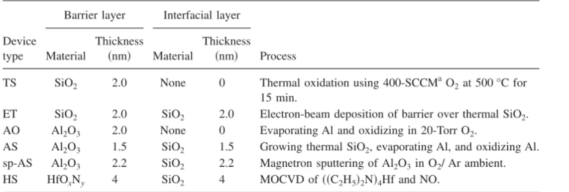
Figure 5 shows the increase of the number N of EL sites as the current I in a forward-biased virgin device increased. The images in Figs. 5共a兲–5共d兲 show a 0.2-mm-diameter sp-AS device subjected to progressive increases in forward bias in a constant-voltage mode. Where the number of EL sites exceeded ten, it was determined automatically using
IMAGEPROmachine-vision software. Manual and automated counts were verified as equivalent for up to 50 sites.
In Fig. 5共e兲 we plot the linear increase of N with I for several virgin devices during the first application of forward bias. Two structures are represented, both with SiO2 interfa-FIG. 4. Micrographs of devices with various barriers and SiO2interfacial
layer.共a兲 Illuminated view, unbiased 0.4-mm-diameter ET device 共SiO2 bar-rier兲. 共b兲–共d兲 Negative EL images for the following forward-biased devices: 共b兲 ET at 9 V and 140 mA; 共c兲 sp-AS 共Al2O3 barrier兲, 12.5 V, 81 mA, 0.2-mm diameter;共d兲 HS 共HfOxNybarrier兲, 7 V, 108 mA, 0.1-mm diameter.
FIG. 5. Number N of EL sites vs forward current I in a virgin device.共a兲–共d兲 Negative images of 0.2-mm-diameter sp-AS device at 22, 47, 66, and 81 mA, respectively.共e兲 N vs I plot. Open symbols: sp-AS devices. Crossed symbols: ET devices. Each shape denotes mesa diameter in millimeter:共䊊兲 0.1,共䉭兲 0.2, 共䊐兲 0.4, and 共〫兲 0.6.
cial layers: sp-AS共Al2O3barrier兲 and ET 共SiO2barrier兲. The
observed behavior was similar regardless of the composition of the insulator layers or the device area. The slope indicates an average current increase of 0.3 mA per light-emitting site. The linear increase suggests that each EL site acted as an antifuse formed by dielectric breakdown. If we assume that the diameter of a breakdown spot was from 100 to 10 nm, the local current density was from 106 to 108 A / cm2,
respectively.
In Fig. 6 we show experimental I-V data for both “vir-gin” devices and stressed devices. We compared the I-V characteristics with the mechanisms presented by Miranda and Suñé.44 The virgin I-V curve for the sp-AS device 共Al2O3barrier兲 is consistent with either stress-induced
leak-age current for small N or soft breakdown for larger N. Di-rect tunneling is expected to make a lesser contribution to the current due to the relatively thick共4.4 nm兲 barrier and inter-facial layers. While no light emission was observed by eye for the virgin sp-AS device, this may simply have been due to the relatively low current.
The current in a sp-AS device following constant-voltage stress for 5 min at 10 V and 100 mA was several orders of magnitude greater than that in the virgin device. A large number of pointlike sites for the visible EL were ob-served in forward bias. The magnitude of current present in the poststress sp-AS I-V curve was similar to the hard break-down examples in Ref. 44. On the other hand, one cannot exclude the soft breakdown occurring at a large number N of sites.
The QPC model has the advantage of being equally ap-plicable to both soft and hard breakdown modes. The heavy line plotted in Fig. 6 is a fit of Eq. 共1兲 to the forward-bias poststress sp-AS I-V curve, with the number of sites and the series resistance as input parameters. We found N⬇200 from a count of EL sites in an image of the device operated at maximum stress. In addition, we found Rseries⬇140 ⍀ for a
0.2-mm-diameter mesa from the slope at a high bias of the I-V curve of an Al–Si Schottky diode that was fabricated on a comparable substrate. The parameters obtained from the fit were ⌽=1.26 V, V0⬇1.53 V, ␣= 5.12 V−1, and = 0.89.
Given the observed color diversity, we emphasize that each site was distinct, so that these parameters are average values. Nevertheless, this particular I-V curve and the values of the parameters obtained from the fit are representative of many
measurements on several sp-AS devices. Qualitatively simi-lar I-V curves can be obtained for other devices that exhibit a pointlike light emission, although the exact fit parameters vary primarily with the insulator thickness and secondarily with the insulator composition. The greatest deviation of the fit from the measured data occurs between about 0.5 and 2.0 V, marking the transition to the series-resistance-limited con-duction at high biases.
The top curve in Fig. 6 represents a TS device with a single 2-nm thermal SiO2 layer. Only a few breakdown events were observed at relatively high biases. Below 4.5 V, the I-V curves for stressed TS devices generally reproduced the virgin curves. The TS device I-V followed the diode equation with ideality factor n = 2.1 up to 0.5 V. A forward-bias operation was accompanied by a dim visible EL that was relatively uniform across the entire mesa, without any pointlike sites. It appears that tunneling through the thin bar-rier was favored over the formation of luminescent break-down sites.
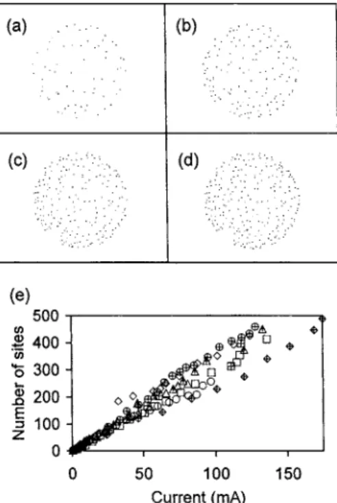
For ET, AO, AS, sp-AS, and HS devices, the Si band-gap peak near 1100 nm was bracketed by emission in a broad range of shorter and longer wavelengths. As an example, the spectra for different forward-bias voltages are presented in Fig. 7 for an ET device. We emphasize that devices were subjected to constant-voltage electrical stress prior to the ac-quisition of EL spectra, so that I-V and other characteristics do not change significantly during the course of the measure-ment. The light intensity varied linearly with current. The external quantum efficiency for the above-gap EL measured for an sp-AS device was about 10−7, in line with expectations
for band-gap Si light emitters. With respect to the power conversion efficiency, using a pW-precision meter, we found that for a 10-V bias and a 100-mA current 共1 W electrical power dissipation兲 the external optical power detected was 10 nW each in the above-gap共Si photodiode兲 and below-gap 共Ge photodiode兲 wavelength ranges. Much of the electrical power dissipation was due to the series resistance of the substrate.
Figure 8 shows the spectrum from a TS device at a for-ward bias of 5 V and a current of 85 mA. Given that the insulator was thinner than in the sp-AS case, the current for a given voltage was higher共see Fig. 6兲, consistent with direct tunneling. No pointlike visible EL was evident. Relative to sp-AS and ET devices, the band-gap EL was strong and the above-gap EL was weak. No below-gap EL was measured at wavelengths longer than about 1300 nm.
FIG. 6. I-V curves. Top: TS device共䊊兲. Middle: data from sp-AS device after stress共䊐兲, with fit to QPC model 共bold line兲. Bottom: virgin sp-AS device共䊏兲.
FIG. 7. Spectra from 0.1-mm-diameter ET device at the following forward-bias levels: 11 V and 72 mA共top兲; 9 V and 49 mA 共middle兲; 7 V and 30 mA 共bottom兲. Features near 700 and 1350 nm are artifacts of the coarse calibration.
054502-6 Mihaychuk et al. J. Appl. Phys. 98, 054502共2005兲
Some sp-AS devices were also made on n-type Si. No pointlike sites for EL were evident, although dielectric break-down features were still present in the I-V curve. For the forward-biased n-type device共ITO at positive potential兲 only the band-gap peak was observed. We therefore emphasize that the broad-spectrum EL was associated primarily with electron injection into p-type Si.
As Fig. 7 shows for the ET device, the spectrum shifted to shorter wavelengths as the forward bias was increased. The shift is consistent with an increase in the energy of elec-trons in the Si CB. By linearly extrapolating the short-wavelength tail to zero intensity, as in Fig. 9共a兲, we were able to estimate the maximum photon energy present. The maxi-mum photon energy, plotted as a function of the forward-bias voltage in Fig. 9共b兲, increased monotonically with the bias for ET, sp-AS, and TS devices. Although the increase in the cutoff photon energy was rapid at low biases, the effect be-gan to saturate by 5 V, where series resistance dominates. An earlier study26 found that the visible spectrum from ITO/ SiO2/Si tunnel diodes was insensitive to biases from about 6
to 9 V; however, the authors did not report results for lower voltages.
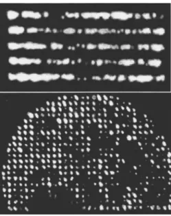
B. Patterned thick-oxide devices
Optical micrographs of patterned devices operated in forward bias, such as those shown in Fig. 10, showed visible EL only in the openings defined using electron-beam lithog-raphy. The color and brightness varied from one location to another in a manner similar to the thin-insulator devices. For the square-array device operated at a 15-V bias and a 100-mA current depicted in Fig. 10, about 400 of the 519 square windows emitted light. In comparison, thin-insulator devices had about 300 pointlike EL sites at the same current. The spectra were similar in form for both patterned and un-patterned devices. Changing the barrier from Al2O3 to
ther-mal SiO2did not significantly alter the behavior.
I-V curves for patterned devices were similar to those for unpatterned devices. For devices with the same number of square windows, the I-V characteristics were independent of the size of the windows, for sizes of 1 µm, 500, 300, or 100 nm. The current at a given voltage varied little despite a hundredfold change in the window area. The similarity of current levels, number of EL sites, and spectra suggests that current flow may have been via breakdown sites in both pat-terned and unpatpat-terned devices. If so, then each square must typically have contained one site with dimensions less than the smallest window size of 100 nm.
In layer structures where unpatterned devices showed pointlike visible EL, patterned devices also showed pointlike EL. Since negligible current was expected to flow through the 18-nm-thick oxide, and the current levels were similar, it is likely that almost all current passed through the light-emitting regions in both cases. As another example of the importance of current concentration in visible EL, patterned devices with a thermal SiO2 insulator produced visible EL
whereas unpatterned TS devices produced little above-gap EL 共Fig. 8兲. Thus visible EL was associated with current concentration, whether at a breakdown site or at a window in a thick SiO2.
FIG. 8. Spectrum from TS device at forward bias of 5 V and 85 mA. Above-gap EL is shown multiplied ten times for clarity.
FIG. 9. Shift of spectrum with increasing forward bias. 共a兲 Short-wavelength EL for sp-AS device from 9 V共top兲 to 5 V 共bottom兲 in 1 V steps. Dashed line, squares: example linear fit to tail at a 7 V bias.共b兲 Maximum photon energy vs bias:共⫻兲 sp-AS, 共䊊兲 ET, 共⫹兲 TS.
FIG. 10. Micrographs of electron-beam-patterned AO devices operated in forward bias. Top: five 1-µm-wide lines, at 11 V and 45 mA. Bottom: array of 1-µm squares, at 15 V and 100 mA, with lower left obscured by the electrical probe tip.
VI. DISCUSSION
We observed broad-spectrum EL from several MIS tun-nel diodes. We found pointlike EL sites in devices with a variety of insulators. The number of sites increased in pro-portion to the forward current, suggesting the formation of breakdown sites. The observations were independent of the growth method used to form the ITO.
It is interesting to compare the spectra associated with pointlike EL 共e.g., ET or sp-AS兲 with devices with more spatially uniform EL 共TS兲. In ET and sp-AS devices, the broad-spectrum EL was enhanced, and the band-gap peak was relatively weak. The converse was true for TS devices. Relative to the ET device operated at 72 mA共see Fig. 7兲, the TS device at 85 mA共see Fig. 8兲 exhibited a ten-fold greater band-gap EL, but a 4.5-times lower integrated EL at wave-lengths less than 900 nm. The measured photon energy ranges at a 5-V bias were 1.0–2.1 eV for the TS device, compared with 0.7–2.4 eV for the ET device.
The variation in the band-gap and broad-spectrum com-ponents leads one to consider the origins of each. Regarding the band-gap EL, an electron tunneling into Si can relax to a state near the CB minimum through multiple electron-phonon scattering events. While a nonradiative recombina-tion with a hole usually follows, a phonon-assisted radiative recombination can sometimes occur. The resulting peak has photon energies slightly below the Si band-gap.
EL at photon energies far from the band-gap is consis-tent with hot-electron radiative transitions in Si. For a suffi-ciently energetic distribution of tunneling electrons, CB-CB or CB-VB EL can span a large range of visible and near-IR photon energies.39In devices on n-type Si we observed only the band-edge EL, which suggests that hot-hole VB-VB pro-cesses are not effective.
Si metal-oxide-semiconductor field-effect transistor 共MOSFET兲 models39–41
predict slowly varying CB-CB EL from 0.5 to 1.0 eV共2480 to 1240 nm兲, similar to what we observed共Fig. 7.兲 A model of our devices should account for tunneling, scattering, drift, and diffusion in the vicinity of a breakdown site with submicron lateral extent. A constraint would be that electrons cool over a distance of not more than several hundred nanometers, based on the apparent size of the visible EL sites.
In devices with a pointlike EL, the enhanced broad-spectrum EL was accompanied by the relatively weak band-gap EL. However, it is not clear if the hot-electron EL would alter the subsequent radiative recombination involving elec-trons near the CB minimum. Instead, the diminished band-gap EL may be associated with the enhanced nonradiative recombination due to an increase in the density of interface states near a breakdown site. While other workers28 have suggested a direct competition between the visible and the band-edge EL, this appears unlikely. Given the low quantum efficiency, the hot-carrier EL only involves a negligible frac-tion of the total number of carriers available to participate in the band-gap EL.
The bias dependence of the high-photon-energy cutoff suggests that the distribution function for electrons in the Si CB undergoes a corresponding shift to higher energies. We
found that the spectrum shifted substantially at a low bias, where the voltage drop due to series resistance is small. It appears that Liu et al. did not observe a similar effect26 be-cause their results were obtained at a relatively high bias, where the effect saturates. The apparent lack of sensitivity to bias led Liu et al. to propose a mechanism for the visible EL involving the recombination of hot electrons and hot holes after the impact ionization. However, impact ionization would produce a quadratic variation of light intensity with current,47 whereas we measured a linear variation.
We also note that our results differed from the models of Asli et al.,48 who predicted that the above- and below-gap EL should be three to five orders of magnitude below the band-gap peak. We found that these features were often com-parable in intensity.
VII. CONCLUSIONS
Using MIS tunnel diodes with ITO transparent elec-trodes, we have explicitly identified and studied EL at sub-micron-sized breakdown sites. Our devices can support hun-dreds of pointlike breakdown sites without a catastrophic failure of the device.
We have also used electron-beam lithography to pattern sites for conduction and EL in thick-oxide devices. By study-ing a variety of structures at both visible and near-IR wave-lengths, we have gained a more complete understanding of the EL phenomena.
In particular we have shown that the band-gap peak can be bracketed at lower and higher photon energies by broad features of similar intensity. For devices where current flow and EL are associated with breakdown sites, the broad-spectrum EL was enhanced and the band-gap EL was dimin-ished, relative to devices with a thin thermal SiO2 barrier.
The spectra were consistent with a combination of the hot-electron radiative transitions and the band-gap recombination.
An important application of light-emission microscopy concerns visualization of leakage current. Scaled MOSFET’s require thicker, low-leakage gate dielectrics. To achieve the desired transconductance high- materials are introduced to maintain the capacitance. EL imaging and spectroscopy can be used to study leakage and breakdown in these materials.
Despite the low external quantum efficiency共⬃10−7兲 of
EL, the small size of the pointlike EL sites may prove useful. Furthermore, the number of sites created for a given current is independent of mesa size, in the range of sizes studied. On this basis it should be possible to make smaller light-emitting devices on Si, using a low-resistivity substrate and/or a shal-low active region to reduce the spreading resistance.
ACKNOWLEDGMENTS
This work was carried out under the NRC-NSCT col-laboration on “RF & Optical Wireless Interconnects for VLSI IC.” We gratefully acknowledge technical assistance from H.T. Tran, P. Ma, J. Lapointe, M. Lee, D. Landheer, X. Wu, J.W. Fraser, S. Moisa, M. Beaulieu, J.M. Fraser, S. Ray-mond, and N. Rowell.
054502-8 Mihaychuk et al. J. Appl. Phys. 98, 054502共2005兲
1D. A. B. Miller, Nature共London兲 384, 307 共1996兲. 2S. S. Iyer and Y.-H. Xie, Science 260, 40共1993兲. 3L. Pavesi, J. Phys.: Condens. Matter 15, R1169共2003兲.
4See, for example, Silicon Photonics, Topics in Applied Physics Vol. 94, edited by L. Pavesi and D. J. Lockwood共Springer, Berlin, 2004兲; Physica E共Amsterdam兲 16 共2003兲; and Intel Technol. J. 8, No. 2 共2004兲 共http:// developer.intel.com/technology/ITJ/兲
5D. A. B. Miller, IEEE J. Sel. Top. Quantum Electron. 6, 1312共2000兲. 6International Technology Roadmap for Semiconductors, http://
public.itrs.net/
7S. Lazarouk, P. Jaguiro, S. Katsouba, G. Masini, S. La Monica, G. Maiello, and A. Ferrari, Appl. Phys. Lett. 68, 1646共1996兲.
8K. D. Hirschman, L. Tsybeskov, S. P. Duttagupta, and P. M. Fauchet, Nature共London兲 384, 338 共1996兲.
9L. Tsybeskov, S. P. Duttagupta, K. D. Hirschman, D. G. Hall, and P. M. Fauchet, Appl. Phys. Lett. 69, 3411共1996兲.
10J. De La Torre et al., Physica E共Amsterdam兲 16, 326 共2003兲. 11A. Irrera et al., Physica E共Amsterdam兲 16, 395 共2003兲. 12A. Polman, J. Appl. Phys. 82, 1共1997兲.
13M. E. Castagna et al., Physica E共Amsterdam兲 16, 547 共2003兲; M. E. Castagna et al., Mater. Sci. Eng., B 105, 83共2003兲.
14Ch. Buchal et al., Nucl. Instrum. Methods Phys. Res. B 190, 40共2002兲. 15Ch. Buchal, S. Wang, F. Lu, R. Carius, and S. Coffa, Nucl. Instrum.
Methods Phys. Res. B 190, 40共2002兲.
16M. A. Green, J. Zhao, A. Wang, P. J. Reece, and M. Gal, Nature共London兲
412, 805共2001兲.
17J. Zhao, M. A. Green, and A. Wang, J. Appl. Phys. 92, 2977共2002兲. 18M. J. Chen, J. L. Yen, J. Y. Li, J. F. Chang, S. C. Tsai, and C. S. Tsai, Appl.
Phys. Lett. 84, 2163共2004兲.
19W. L. Ng, M. A. Lourenco, R. M. Gwilliam, S. Ledain, G. Shao, and K. P. Homewood, Nature共London兲 410, 192 共2001兲.
20M. du Plessis, H. Aharoni, and L. W. Snyman, IEEE J. Sel. Top. Quantum Electron. 8, 1412共2002兲.
21M. Lahbabi et al., Appl. Phys. Lett. 77, 3182共2000兲.
22A. T. Obeidat, Z. Kalayjian, A. G. Andreou, and J. B. Khurgin, Appl. Phys. Lett. 70, 470共1997兲.
23J. C. Tsang, J. A. Kash, and D. P. Vallet, Proc. IEEE 88, 1440共2000兲. 24C. Leroux and D. Blachier, Microelectron. Eng. 49, 169共1999兲. 25A. Chatterjee and B. Bhuva, IEEE Trans. Device Mater. Reliab. 2, 60
共2002兲.
26C. W. Liu, S. T. Chang, M. J. Chen, and C. F. Lin, Appl. Phys. Lett. 77,
4347共2000兲.
27A. Chin, C. S. Liang, C. Y. Lin, C. C. Wu, and J. Liu, IEDM Technical
Digest, International Electron Devices Meeting, 2001, Washington, D. C.,
2–5 December 2001共IEEE, Piscataway, NJ, 2001兲, p. 171.
28E. Cartier, J. C. Tsang, M. V. Fischetti, and D. A. Buchanan, Microelec-tron. Eng. 36, 103共1997兲.
29M. J. Chen, C. F. Lin, W. T. Liu, S. T. Chang, and C. W. Liu, J. Appl. Phys. 89, 323共2001兲.
30Y. Q. Wang, T. P. Zhao, J. Liu, and G. G. Qin, Appl. Phys. Lett. 74, 3815 共1999兲.
31C. Y. Lin, A. Chin, Y. T. Hou, M. F. Li, S. P. McAlister, and D. L. Kwong, IEEE Photon. Technol. Lett. 16, 36共2004兲.
32R. Versari, A. Pieracci, M. Manfredi, G. Soncini, P. Bellutti, and B. Ricco,
IEDM Technical Digest, International Electron Devices Meeting, 1999,
Washington, D.C., 5–8 December 1999共IEEE, Piscataway, NJ, 1999兲, p. 745.
33L. Heikillä, T. Kuusela, and H.-P. Hedman, J. Appl. Phys. 89, 2179 共2001兲.
34N. Porjo, T. Kuusela, and L. Heikillä, J. Appl. Phys. 89, 4902共2001兲. 35M. J. Chen, J. F. Chang, J. L. Yen, C. S. Tsai, E. Z. Liang, C. F. Lin, and
C. W. Liu, J. Appl. Phys. 93, 4253共2003兲.
36M. J. Chen, E. Z. Liang, S. W. Chang, and C. F. Lin, J. Appl. Phys. 90, 789共2001兲.
37C. W. Liu, M. H. Lee, M. J. Chen, I. C. Lin, and C. F. Lin, Appl. Phys. Lett. 76, 1516共2000兲.
38M. Rasras, I. De Wolf, G. Groeseneken, R. Degraeve, and H. E. Maes, J. Appl. Phys. 91, 2155共2002兲.
39M. Pavesi, P. L. Rigolli, M. Manfredi, P. Palestri, and L. Selmi, Phys. Rev. B 65, 195209共2002兲.
40S. Villa, A. L. Lacaita, and A. Pacelli, Phys. Rev. B 52, 10993共1995兲. 41J. Bude, N. Sano, and A. Yoshii, Phys. Rev. B 45, 5848共1993兲. 42J. R. Goldman and J. A. Prybyla, Phys. Rev. Lett. 72, 1364共1994兲. 43D. F. Edwards, in Handbook of Optical Constants of Solids, edited by E.
D. Palik共Academic, Orlando, 1985兲, pp. 547–569.
44E. Miranda and J. Suñé, Microelectron. Reliab. 44, 1共2004兲. 45E. Miranda and J. Suñé, Microelectron. Reliab. 40, 1599共2000兲. 46D. K. Schroder, Semiconductor Material and Device Characterization,
2nd ed.共Wiley, New York, 1998兲, Chap. 3.4, p. 143.
47G. Deboy and J. Kölzer, Semicond. Sci. Technol. 9, 1017共1993兲. 48N. Asli, A. F. Shulekin, P. D. Yoder, M. I. Vexler, I. V. Grekhov, and P.
Seegebrecht, Solid-State Electron. 48, 731共2004兲.