Low Power On-Chip Current Monitoring
Medium-Grained Adaptive Voltage Control
Wei-Chih Hsieh and Wei Hwang, Fellow, IEEE
Department of Electronics Engineering & Institute of Electronics, and Microelectronics and Information Systems Research Center,
National Chiao-Tung University, Hsin-Chu 300, Taiwan
[email protected], [email protected]
Abstract—In this paper, a novel low power on-chip current
monitor is proposed for adaptive voltage control (AVC). Instead of tracking the delay of worst case critical path replica, current characteristic of target circuits is considered. The proposed current monitor distinguishes between the switching and stable state of the circuit by monitoring the current consumption. It has no negative impact on circuit speed with only less than 3µW power overhead. Using proposed low power on-chip current monitor, a medium-grained adaptive voltage control scheme is also presented. Traditional AVC applied a single (scaled) voltage satisfying critical path to the whole chip, wasting the power in non-critical paths. The medium-grained AVC exploits the unused slack in non-critical paths, which further discovers the power reduction potentiality that lies on non-critical paths. A different width multipliers example exhibits over 30% power reduction on non-critical paths. Simulations are all implemented in Berkeley Predictive 65nm technology [7].
I. INTRODUCTION
New technology has encouraged the System-on-a-Chip (SoC) style design and a tremendous boost of integrated circuits on a single die. The ever increasing amount of power consumption coming along has become a serious design issue in SoC era. Therefore, controlling and further reducing the power consumption is an urgent design consideration for nowadays technology.
Voltage scaling has been suggested to be an efficient power reduction method due to its quadratic relation in the power equation. Adaptive voltage scaling (AVS) or dynamic voltage scaling (DVS) with critical path replica scheme is the most used method [1]-[3]. Delay synthesizer [1] was proposed to emulate gate delay, RC interconnection delay, and rise/fall delay at a time. Ring oscillator [3] had been suggested to track the critical path as well as the process and temperature variations. However, the mostly used critical path method has some inherited limitation. It always tracks the worst case critical path delay, which is not frequently occurred during the chip operation. Moreover, safety
margins are added in order to ensure that the critical path replica fails before the chip. In addition, though the critical path replica ensures the correctness of the whole chip, energy in those non-critical paths has been wasted. These considerations limit the efficiency of the voltage scaling.
A low power on-chip current monitoring scheme is proposed for AVS. This on-chip current monitoring scheme needs no critical path replica, therefore significantly reduces the voltage scaling overhead. The scheme can aggressively scale down the supply voltage while maintaining the correct operation of the logic. The voltage safety margin is also eliminated. Moreover, due to the low overhead of the proposed current monitoring scheme, the voltage scaling can be applied even deeper into the non-critical paths. This medium-grained adaptive voltage control mechanism further discovers the power reduction potentiality that lies on the non-critical paths.
This paper is organized as follows. The design concept of current monitoring scheme is derived in Section II. The proposed low power on-chip current monitoring adaptive voltage control is presented in Section III. The medium-grained adaptive voltage control mechanism using the proposed low power on-chip current monitor is briefly described in Section IV. The simulation results are shown in Section V. Finally, Section VI ends with conclusions.
II. DESIGN CONCEPT
Fig. 1 illustrates the current drawn from an ideal power supply by a 16*16 multiplier. It can be observed that the multiplier draws a great amount of current during switching periods such that it exhibits sharp transient current peaks. When the results have been computed successfully, the multiplier enters a stable state without drawing any charging/discharging current except the leakage current.
Supply current will have an upper limit if realistic power supply is used. The drawn current will have lower peak value but wider switching period compared with the one shown in
This research is supported by National Science Council, R.O.C., under project NSC 94-2220-E-009-011, NSC 94-2220-E-009-024. This work also supported by Ministry of Economic Affairs, R.O.C., under the project MOEA 95-EC-17-A-01-S1-034. The authors would like to thank Ministry of Education, ITRI, and TSMC for their support.
1637
A[15:0] B[15:0] Product[15:0] I(VDD) Switching Switching Stable Stable
Figure 1. Current characteristic with respect to circuit switching.
Fig. 1, indicating slower circuit speed. The situation will be worse if the supply voltage is lowered, i.e. speed of the circuit will degrade when the voltage scaled down as suggested in [5]. In other words, to have success computing, the period of stable state of the circuit should be identified and ensured to be longer than a certain time. The current monitoring scheme is then developed to identify the amount of the drawing current from power source and to distinguish between the switching and stable state.
III. LOW POWER ON-CHIP CURRENT MONITORING
ADAPTIVE VOLTAGE CONTROL
The control loop of the current monitoring adaptive voltage scaling is shown in Fig. 2. The loop begins at the power source of the CMOS circuit provided by the voltage regulator. The current monitor block identifies the current characteristic. Processed information will be passed to the AVS control block. Finally a control word is sent back to the voltage regulator to adjust the voltage. The control loop responds every clock cycle.
A. Voltage Regulator
The voltage regulator used here is an on-chip digital power supply [4]. The on-chip digital power supply is implemented as a parallel-connected power switch network, as shown in Fig. 3. This power switch network has multiple resistance values hence provides different voltage levels. A control word (Ctrl[0] ~ Ctrl[4]) controls the on/off state of each power switch. Switches turned on and off sequentially in the order of indexes. Larger indexed switch is turned off first while smaller indexed on first. When the last switch (controlled by Ctrl[0]) is off, the circuit is power gated.
B. Low Power On-Chip Current Monitor
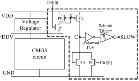
An on-chip transient current monitor [6] was presented to make uses of the power line resistance to sense supply current. The digital power supply is also a resistance network. However, the resistance of the digital power supply and the voltage drop are more than simply correlated. Therefore, a new low power on-chip current monitor is proposed to have better monitor performance. The proposed low power current monitor is depicted in Fig. 4. It consists of a current mirror, a mirror load, a p-skewed inverter, and a Schmitt trigger.
All the power switches work in the linear region. The current provided by each power switch is proportional to its drain-source voltage difference, which is dependent on the value of VDDV. The VDDV will be pulled down more for fewer
CMOS circuit GND Voltage Regulator VDD VDDV Current Monitor Block AVS Control Block
Figure 2. Block diagram of the current monitoring adaptive voltage control loop. CMOS circuit GND VDD VDDV Ctrl[4] Ctrl[3] Ctrl[2] Ctrl[1]Ctrl[0]
Figure 3. On-chip digital power supply [4].
on power switches to supply the same switching current. The value of VDDV rises back to a higher value when fewer
current is required in the stable state. Therefore the value of VDDV varies according to the current characteristics.
The reference of the current mirror is inserted between VDD and VDDV lines. Similar to [6], the proposed current
monitor makes use of the voltage difference of the VDD and
VDDV. However, this voltage difference doesn’t produce a
current difference [6] but is used to control the magnitude of the reference current. P2 mirrors the current and is loaded with a weak long channel N0. P1 and N1 are used to turn off the current monitor when the circuits are power gated, otherwise the current mirror will consume power in gating period and increase the power overhead.
The monitor is asked to assert only when VDDV is lower
than a safe level. When VDDV is pulled too low, it will
produce a large mirrored current. The voltage level of node C will rise above a configured value. A p-skewed inverter is used to respond at the point. Schmitt trigger generates “SLOW” signal with hysteresis threshold and fast transient response. The simulation results of proposed current monitor are shown in Fig. 6. “SLOW” signal is used by AVS control block as described in III.C.
The reference current through P0 and P1 is also used for circuit switching, not wasted in vain as in [6], therefore reduces the power overhead of the current monitor. This compensation of switching current makes proposed current monitor to have no negative impact on the circuit speed.
C. Adaptive Voltage Control Block
The control block is a finite state machine responding every clock cycle. It monitors the SLOW signal. No SLOW signal means present voltage state exceeds corresponding requirement, and the controller will instruct the power switch network going to next weaker state to save the power consumption. If the SLOW signal is asserted, the voltage state is raised to speed up the circuit. In order to have a more 1638
VDDV CMOS circuit GND Voltage Regulator VDD Ctrl[0] Ctrl[0] P0 P1 P2 N0 N1 p-skewed INV Schmitt Trigger SLOW C X
Figure 4. Proposed low power current monitor.
stable control, there can be cycles between each adjustment. The interval setting is a trade-off between stability and power reduction aggressiveness.
D. Design Priciple of Current Monitor
P0 is always in saturation region while P1 in linear region. Using the same (W/L) ratio of P0 and P1, VX can be
determined by
(
)
(
)
DD tp DDV DD tp DDV tp DD X V V V V V V V V V + + + + + = 2 2 1 2 2 2 (1) where Vtp is PMOS threshold voltage. It’s obviously that VXrelates only to one variable VDDV as what is desired. On the
other hand, P2 and N0 are both in saturation region, the relation between VC and VX can be given by
(
)
(
(
)
)
(
)
2 0 ' 2 ' 2 tp DD X N n P p tn C V V V L W k L W k V V − = − − (2)where Vtn is NMOS threshold voltage, k’ is the process
transconductance parameter. It can be shown in (2) that VC,
VX and (W/L) ration of P2 and N0 are correlated.
A simple α power model suggested that the delay varies with supply voltage as [5]
(
)
α th DD DD g V V V K T − = (3)where K is a proportional constant specific to a given technology, and α is the velocity saturation coefficient. Therefore, the calibration of proposed current monitor starts from determining the original and largest allowable scaled delay of the target circuit block. The lowest allowable VDDV
(VLow) will be derived by scaled delay ratio using (3). This
VLow is a response point for the current monitor. Some
margins can be added to have safer operation and to tolerate the response time of current monitor. The critical VX can be
derived by putting VLow in (1). The critical VC when VDDV
32*32 Mult. 16*16 Mult. FF LCFF FF AVS
Figure 5. A simple example of proposed medium-grained adaptive voltage control. LC represents pass-transistor half latch level converters.
reaches the critical point can be chosen arbitrarily. Then the (W/L) ratio of P2 and N0 can be determined by putting critical VX and VC together into (2). The switching threshold
of p-skewed inverter and Schmitt trigger can also be derived from critical VC.
The overhead comes from mirrored current, inverter, and Schmitt trigger, and mostly from the latter two. The mirrored current is determined by (W/L) ratio of P0 and P2, while the critical VC only depends on (W/L) ratio of P2 and N0.
Therefore the mirrored current can be greatly suppressed with long length narrow width transistors. The inverter and Schmitt trigger are sized as small as possible to reduce the power overhead.
IV. MEDIUM-GRAINED ADAPTIVE VOLTAGE CONTROL
Traditional AVS applies a single (scaled) voltage to the whole chip. The voltage can only be scaled down to the lowest level for critical paths to function correctly. However, there is still much power reduction potentiality on non-critical paths. A medium-grained adaptive voltage control using presented low overhead current monitoring scheme is proposed to exploit it.
A simple example is shown in Fig. 5 to exhibit the proposed medium-grained adaptive voltage control. Suppose the supply voltage is just sufficient for the 32*32 multiplier under a certain cycle time. However, the 16*16 multiplier requires much less than that to come out with the result under the same voltage level. The medium-grained adaptive voltage control is applied to exploit the unused slack of the 16*16 multiplier.
Fig. 5 takes two different function blocks as an example. However, the medium-grained adaptive voltage control can apply on any types of non-critical paths. The overhead comes from current monitor, controller, and level converters. These overheads are negligible if the target is more than an order of magnitude larger. This is not so difficult since the overhead of proposed scheme is quite small. The proposed scheme is therefore called medium-grained adaptive voltage control. Moreover, different groups of non-critical paths can have different controllers, resulting in better adaptive performance of voltage scaling.
V. SIMULATION RESULTS
Simulations of proposed current monitor and medium-grained adaptive voltage control are all done with Berkeley Predictive 65nm CMOS technology [7].
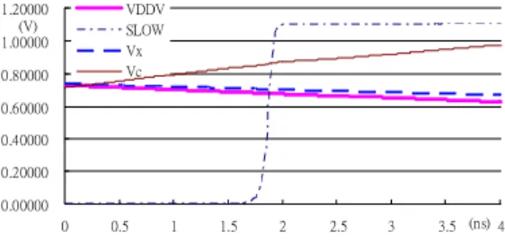
0.00000 0.20000 0.40000 0.60000 0.80000 1.00000 1.20000 0 0.5 1 1.5 2 2.5 3 3.5 (ns)4 (V) VDDV SLOW Vx Vc
Figure 6. Waveform of VDDV, VX, VC, and SLOW signals.
0 0.5 1 1.5 2 2.5 original avs 31.63% 5.04% Original AVS (mW) controller level converters monitor 16*16 mult.
Figure 7. Simulation Results of medium-grained adaptive voltage control.
A. Current Monitor
Two parameters are first chosen. The critical VLow and
VC are set at 0.65V and 0.9V, respectively. The critical VX is
0.69V from (1). The switching point of p-skewed inverter is the same as the critical VC. Schmitt trigger is sized to have
lower power with acceptable transient speed.
Fig. 6 shows the simulated waveform of proposed current monitor. It can be observed that VC rises above 0.9V and
SLOW signal asserts when VDDV is lower than 0.65V. VX is
slightly higher than VDDV at the point. The simulation results
match with the first order equations in III.D pretty well. The power overhead of the proposed current monitor is less than 3µW depending on applications. This overhead is quite low.
B. Medium-Grained Adaptive Voltage Control
The simulation environment is set up as shown in Fig. 5. The cycle time is 2ns, which is the minimum cycle time that the 32*32 multiplier required. However, this 2ns cycle time is more than enough for the 16*16 multiplier. Proposed medium-grained adaptive voltage control is applied on the 16*16 multiplier. The simulation results are shown in Fig. 7, including original circuits’ results without voltage scaling.
As shown in Fig. 7, with medium grained adaptive voltage control the non-critical 16*16 multiplier’s power has reduced about 36%. The adaptive voltage control has introduced only 5% power overhead, most of which comes from un-optimized level converters. Considering the 32*32 multiplier and flip-flops’ power consumption, this example only has a 5.82% power reduction. However, it has been stated that this medium scheme can be applied more than
once in a chip. Multiple groups of non-critical paths will accumulate this reduction percentage.
VI. CONCLUSIONS
A new low power current monitor for adaptive voltage control is proposed in this paper. Traditional critical path replica scheme results in quite conservative power reduction. Proposed scheme makes use of current monitoring to distinguish whether the circuits have entered the stable state. The proposed scheme scales the voltage according to actual circuit operation instead of a predefined worst case condition. The proposed current monitor consists of a current mirror, a p-skewed inverter, and a Schmitt trigger. The reference current of the current mirror exhibits a compensation for the switching current, imposing no extra power overhead. The attached current mirror has no speed impact on the circuit, neither. The power overhead of the proposed current monitor is less than 3µW.
Presented low power current monitor helps the voltage scaling to be applied even deeper into non-critical paths. A medium-grained adaptive voltage control is proposed. Unlike traditional method wasted power on non-critical paths, proposed medium-grained adaptive voltage control further discovers the power reduction potentiality that lies on non-critical paths. Simulation shows that the medium-grained adaptive voltage control on an example of multipliers reduces more than 30% of power on non-critical paths. Moreover, the medium-grained adaptive voltage control suggests that multiple different controllers can be attached to different groups of non-critical paths. Each group can scale voltage independently for best operating point, which results in better adaptive performance of voltage scaling.
REFERENCES
[1] M. Nakai, S. Akui, K. Seno, T. Meguro, T. Seki, T. Kondo, A. Hashiguchi, H. Kawahara, K. Kumano, and M. Shimura, “Dynamic Voltage and Frequency Management for a Low-Power Embedded Microprocessor,” IEEE Journal of Solid-State Circuits, vol. 40, no. 1, pp. 28-35, Jan. 2005.
[2] M. Nomura, Y. Ikenaga, K. Takeda, Y. Nakazawa, Y. Aimoto, and Y. Hagihara, “Delay and Power Monitoring Schemes for Minimizing Power Consumption by Means of Supply and Threshold Voltage Control in Active and Standby Modes,” IEEE Journal of Solid-State
Circuits, vol. 41, no. 4, pp. 805-814, April 2006.
[3] T. D. Burd, T. A. Pering, A. J. Stratakos, and R. W. Brodersen, “A Dynamic Voltage Scaled Microprocessor System,” IEEE Journal of
Solid-State Circuits, vol. 35, no. 11, pp. 1571-1580, Nov. 2000.
[4] M. Meijer, J. P. de Gyvez, and R. Otten, “On-Chip Digital Power Supply Control for System-on-Chip Applications,” Proceedings of
the 2005 International Symposium on Low Power Electronics and Design, Aug. 2005, pp. 311-314.
[5] R. Gonzalez, B. M. Gordon, and M. A. Horowitz, “Supply and Threshold Voltage Scaling for Low Power CMOS,” IEEE Journal of
Solid-State Circuits, vol.32, no. 8, pp. 1210-1216, Aug. 1997.
[6] V. Stopjaková, H. Manhaeve and M. Sidiropulos, “On-chip Transient Current Monitor for Testing of Low-Voltage CMOS IC,” Proceedings of Design, Automation and Test in Europe Conference and Exhibition, Mar. 1999, pp. 538-542.
[7] Berkeley Predictive Technology Model (BPTM),
http://www.eas.asu.edu/~ptm/ .
![Figure 2. Block diagram of the current monitoring adaptive voltage control loop. CMOS circuit GND VDDVDDVCtrl[4]Ctrl[3]Ctrl[2]Ctrl[1]Ctrl[0]](https://thumb-ap.123doks.com/thumbv2/9libinfo/7666596.140919/2.918.83.455.112.231/figure-diagram-current-monitoring-adaptive-voltage-control-vddvddvctrl.webp)