threshold voltage (DT) MOSFETs are experimentally examined. In the low-voltage regime, both the cutoff and maximum oscilla-tion frequencies ( and max) tend to increase with temperature. In addition, the inherent body-related parasitics and the series resistance have much more impact on max than . Besides, we found that the noise stemmed from the body resistance( ) would contribute to the output noise current, and degrade the minimum noise figure(NFmin). Our study may provide insights
for RF circuit design using advanced SOI DT MOSFETs. Index Terms—Body resistance, dynamic threshold voltage (DT) MOSFETs, noise, RF, silicon-on-insulator (SOI), small signal, tem-perature dependence.
I. INTRODUCTION
D
UE TO its larger current driving ability with low leakage current, the dynamic threshold voltage (DT) MOSFET is attractive for low-power applications [1]. Hence, the dc char-acteristics and modeling of the DT MOSFET have been widely studied since its introduction [2]–[4]. Moreover, the temperature effect on its dc characteristic has also been well investigated [4]. Several optimized silicon-on-insulator (SOI)- or bulk-based DT MOS fabrication processes with improved performance have been demonstrated [5], [6], and its ability of RF applica-tions with high cutoff frequency and maximum oscillation frequency has been reported as well [7]–[9]. However, the temperature effect on the RF characteristics of DT MOS-FETs is rarely known.Manuscript received March 02, 2010; revised April 06, 2010; accepted June 08, 2010. Date of publication August 03, 2010; date of current version September 10, 2010. This work was supported in part by the National Science Council of Taiwan.
S.-C. Wang and G.-W. Huang are with the National Nano Device Laborato-ries (NDL), Hsinchu 300, Taiwan, and also with the Department of Electronics Engineering, National Chiao Tung University, Hsinchu 300, Taiwan (e-mail: scwang@ndl.org.tw; gwhuang@ndl.org.tw).
P. Su is with the Department of Electronics Engineering and Institute of Electronics, National Chiao Tung University, Hsinchu 300, Taiwan (e-mail: pinsu@mail.nctu.edu.tw).
K.-M. Chen, K.-H. Liao, and B.-Y. Chen are with the National Nano De-vice Laboratories (NDL), Hsinchu 300, Taiwan (e-mail: kmchen@ndl.org.tw; khliao@ndl.org.tw; bychen@ndl.org.tw).
S.-Y. Huang and C.-C. Hung are with the United Microelectronics Corpo-ration (UMC), Hsinchu 300, Taiwan (e-mail: Samny_Huang@umc.com; Big-choug_Hung@umc.com).
Color versions of one or more of the figures in this paper are available online at http://ieeexplore.ieee.org.
Digital Object Identifier 10.1109/TMTT.2010.2057175
low gate overdrive region. Therefore, it is crucial to examine the RF small-signal and noise characteristics under this regime.
This paper is an experimental investigation on the RF small-signal and noise characteristics of SOI DT MOSFETs and is organized as follows. The measurement environment and device structures/geometries are described in Section II. In Section III, the temperarue effect of body-related parasitics and series resistances on and will then be investigated. In Section IV, the RF noise behavior and its temperature de-pendence will be discussed for the first time. The temperature dependences of the equivalent thermal resistance and minimum noise figure will be examined as well. Finally, conclusions will be drawn in Section V.
II. DEVICES ANDEXPERIMENTS
The RF SOI DT MOSFETs used in this work were fabricated using UMC 65-nm SOI technology. These RF devices were laid out in the multifinger (eight fingers) and multigroup (16 groups) structure with 1- m channel width per finger.
On-wafer two-port common-source high-frequency and noise parameters were measured using an ATN NP5B noise measurement system with Cascade microwave probes. Besides, to eliminate the inevitable parasitic accompanied with the probing pads, the -parameters of the devices’ corresponding dummy were measured and then used to perform the and noise parameters’ de-embedding procedure.
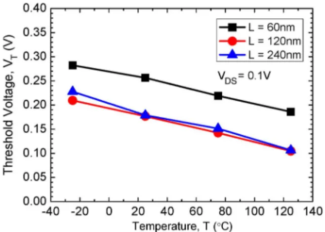
Fig. 1 shows the temperature dependences of threshold voltage extracted by the constant current
nA W/L method. Due to the negative temperature coefficient of the device’s Fermi potential [4], exhibits the negative temperature dependence for each channel length device.
The equivalent circuit for both RF small-signal and noise be-haviors is depicted in Fig. 2. The inherent body-related para-sitics include the source- and drain-side junction capacitances ( and , respectively), the junction resistance , the body resistace , and the body-transconductance . The series resistances , , and were determined using the proposed zero method [10], and the other parameters along with the channel noise current can be extracted by the ex-traction method presented in [11]. Note that to keep the device
2320 IEEE TRANSACTIONS ON MICROWAVE THEORY AND TECHNIQUES, VOL. 58, NO. 9, SEPTEMBER 2010
Fig. 1. Temperature dependence of the threshold voltage for SOI DT MOS-FETs.
Fig. 2. RF small-signal and noise equivalent circuit for the SOI DT MOSFET.
operating in the saturation region, we let in our experiments.
III. RF SMALL-SIGNALCHARACTERIZATION
The cutoff frequency and maximum oscillation fre-quency are two common figures of merit used to characterize the RF performance of a device. Based on the equivalent circuit shown in Fig. 2 and neglecting the series resistances , , and , the “intrinsic” and for the DT MOSFET biased in the low regime can be approximately expressed as the following [12]:
(1) (2) In (1) and (2), , (3) and (4)
Fig. 3. (a) Short-circuit current gainjH j and (b) unilateral power gain U with and without considering the series resistance effect (symbols: measured data; solid and dash lines: modeled results with and without considering the series resistance effect, respectively).
where is the input resistance, which can be extracted by op-timizing .
The approximation in (1) and (2) holds in the low regime, where , , , and around .
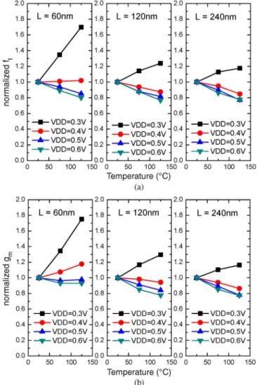
Equation (1) implies that the inherent body-related parasitics of the DT MOSFET would have little influence on . In the low regime, since tends to increase with temperature [4], [13], would have a positive temperature coefficient. On the other hand, due to the less temperature-dependent behavior of and the degradation factor , tends to have the same temperature dependence as [12]. That is, in the low regime, both intrinsic and would increase with temperature.
To investigate the overall performance, however, the impact of the series resistance effect on and should be exam-ined. Fig. 3 shows that the series resistance has much more sig-nificant effect on the unilateral power gain (involved in the determination of ) than the short-circuit current gain (involved in the determination of ) at V. Com-pared to the series resistances, the much larger input and output impedance in the low regime would dominate , and hence, . The little series resistance effect on can be also deduced from Fig. 4(a) and (b), where has nearly the same temperature coefficient as for each channel length device.
Fig. 4. Temperature dependences for: (a)f and (b) g . (Data normalized with respect to their corresponding values atT = 25 C.)
This coincides with the implication in (1), which has assumed the series resistance is insignificant.
The input and output impedance matching for the maximum available power gain, and hence, , however, can be greatly influenced by the series resistances. Moreover, since the degra-dation factor is found to be nearly temperature indepen-dent for each channel length device, as shown in Fig. 5(a), the degraded temperature dependence of , shown in Fig. 5(b), would be mostly caused by the series resistance effect. That is, the larger resistances at higher temperatures would severely de-grade .
IV. RF NOISECHARACTERIZATION
A. Channel Noise and Equivalent Thermal Resistance
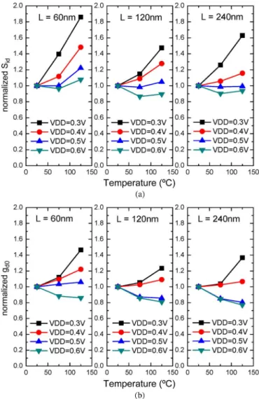
The extracted power spectral density for the channel noise current (denoted as ) is shown in Fig. 6, and is usually expressed as follows [14]:
(5) where J/K is the Boltzmann constant, is the ambient temperature in kelvin, is the channel con-ductance at zero drain–source voltage, and is the noise factor.
Fig. 5. Temperature dependences for: (a) and (b)f . (Data normalized with respect to their corresponding values atT = 25 C.)
Fig. 6. Channel noise versus VDD.
Besides, [15] has shown that has a weak temperature depen-dence, and the temperature dependence of is dominated by that of and .
Fig. 7(a) and (b), respectively, shows the temperature depen-dences of and . In the low regime, since tends to increase with temperature [12], would increase accord-ingly as predicted by (5). Note that (5) was originally derived for the device operating in the strong inversion region. However,
2322 IEEE TRANSACTIONS ON MICROWAVE THEORY AND TECHNIQUES, VOL. 58, NO. 9, SEPTEMBER 2010
Fig. 7. Temperature dependences for: (a)S and (b) g . (Data normalized with respect to their corresponding values atT = 25 C.)
in our experiments, the consistent prediction results for the tem-perature dependence of shows that it seems to remain valid even for the medium or weak inversion applications.
The channel noise has a significant effect on the equivalent thermal resistance for conventioanl MOSFETs. In fact, by neglecting the body trans-conductance, for DT MOSFETs would be approximately the same as that for conventional MOS-FETs as expressed in the following:
(6) where K is the reference temperature. Note that (6) indicates that in the low regime, the body-related para-sitics would have little influence on .
Fig. 8(a) shows versus temperature curves for each channel length device. Since for nm device is about 0.1 V higher than those for nm and nm devices in the whole temperature range (see Fig. 1), we first consider V for nm and nm devices, and V for the nm device to keep approximately the same gate overdrive voltage. In this case, one can compare the temperature dependence for in
Fig. 8. Temperature dependences for: (a)R and (b) g . (Data normalized with respect to their corresponding values atT = 25 C.)
Fig. 7(a) and that for in Fig. 8(b). Since tends to have the similar temperature coefficient as , according to (6), tends to increase with temperature mainly due to the increase of and .
For an nm device operating at weaker bias condition, i.e., V; however, tends to more deeply increase with increasing temperature than . This could compete with or even overwhelm the contribution from “hot” . Therefore, tends to decrease with increasing temperature. This also shows the existence of the zero temperature coefficient for , which occurs between V and V for the nm device.
B. Output Noise Current and Minimum Noise Figure
Unlike , the minimum noise figure may be strongly influenced by . Although the analytical expression for is not easily derived, the noise contribution arising from to the output noise current flowing into the drain terminal can be analyzed and regarded as an important factor determining
.
The noise power spectral density arising from (denoted as ) is considered as thermal noise, and can be expressed as follows:
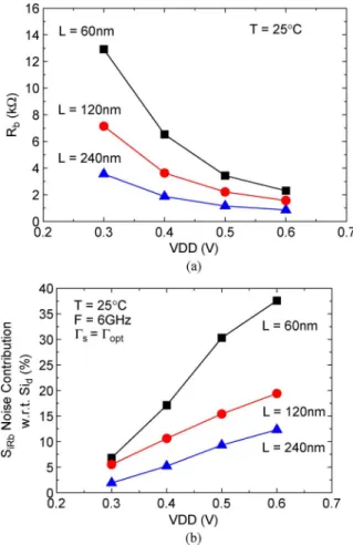
Fig. 9. (a) Extracted body resistance as a function ofV DD. (b) Noise contri-bution from the body noiseS to the output noise current with respect to that from the channel noise.
The extracted values and their corresponding contri-bution with respect to counterpart to the output noise current and are shown in Fig. 9(a) and (b), respectively. We found that larger in the low regime would have less noise contribution for each length device. This figure also shows that the shorter device with larger would have more contri-bution. It is worth noting that the smaller body cross-sectional area seen in the direction perpendicular to the channel current flow can account for the larger present in the shorter device.
Through the sensitivity analysis of the variation of to its noise contribution, as shown in Fig. 10, we can see that its noise contribution could be reduced with increasing . In fact, the noise equivalent circuit for DT MOSFETs would be equiva-lent to that for conventional MOSFETs when approaches infinity and can be removed in the equivalent circuit. Therefore, the larger would play an insignificant role in determining
.
The minimum noise figure versus is shown in Fig. 11. is sharply increased towards the weak inversion region, and this trend is consistent with that for the conventional bulk MOSFET [16]. Moreover, our experimental results show that has less temperature dependence in the low regime. As shown in Fig. 10, in the low regime, since the noise contribution of to the output noise current for each temperature is not significant, would have little effect on the temperature dependence of .
Fig. 10. Sensitivity analysis of the body resistance with respect to its noise contribution.
Fig. 11. NF as a function ofV DD at different temperatures for various channel length devices. (Data normalized with respect to their corresponding values atT = 25 C.)
V. CONCLUSIONS
We have investigated the temperature dependences of RF small-signal and noise behaviors for the DT MOSFET. In the low regime, since tends to increase with temperature, would have a positive temperature coefficient. On the other hand, due to the less temperature-dependent behavior of and , is found to increase with temperature as well. Moreover, the body-related parasitics and the series resistances are found to have more impact on than .
In the low regime, the channel noise has a posi-tive temperature coefficient due to larger at higher tempera-ture. In addition, compared to , the much higher toward the weaker inversion region can cause to have a negative temperature coefficient. Finally, it shows that, in the low regime, the large would have little impact on the temperature dependence of .
ACKNOWLEDGMENT
The authors would like to thank the United Microelectronics Corporation (UMC), Hsinchu, Taiwan, for providing the devices used in this study.
2324 IEEE TRANSACTIONS ON MICROWAVE THEORY AND TECHNIQUES, VOL. 58, NO. 9, SEPTEMBER 2010
REFERENCES
[1] F. Assaderaghi, D. Sinitsky, S. A. Parke, J. Bokor, P. K. Ko, and C. Hu, “Dynamic threshold-voltage MOSFET (DTMOS) for ultra-low voltage VLSI,” IEEE Trans. Electron Devices, vol. 44, no. 3, pp. 414–422, Mar. 1997.
[2] S. S. Rofail and K. S. Yeo, “Experimentally-based analytical model of deep submicron LDD MOSFETs in a Bi-MOS hybrid-mode environ-ment,” IEEE Trans. Electron Devices, vol. 44, no. 9, pp. 1473–1482, Sep. 1997.
[3] J. B. Kuo, K. H. Yuan, and S. C. Lin, “Compact threshold-voltage model for short-channel partially-depleted (PD) SOI dynamic-threshold MOS (DTMOS) devices,” IEEE Trans. Electron Devices, vol. 49, no. 1, pp. 190–196, Jan. 2002.
[4] J.-K. Lee, N.-J. Choi, C.-G. Yu, J.-P. Colinge, and J.-T. Park, “Tem-perature dependence of DTMOS transistor characteristics,” Solid State Electron., vol. 48, pp. 183–187, 2004.
[5] C. Wann, F. Assaderaghi, R. Dennard, C. Hu, G. Shahidi, and Y. Taur, “Channel profile optimization and device design for low-power high-performance dynamic threshold MOSFET,” in Int. Electron. Device Meeting Tech. Dig., Dec. 1996, pp. 113–116.
[6] A. Shibata, T. Matsuoka, S. Kakimoto, H. Kotaki, M. Nakono, K. Adachi, K. Ohta, and N. Hashizume, “Ultra low power supply voltage (0.3 V) operation with extreme high speed using bulk dy-namic threshold voltage MOSFET (B-DTMOS) with advanced fast-signal-transmission shallow well,” in Proc. VLSI Technol. Tech. Symp. Dig., 1998, pp. 76–77.
[7] Y. Momiyama, T. Hirose, H. Kurata, K. Goto, Y. Watanabe, and T. Sugii, “A 140 GHz f and 60 GHz f DTMOS integrated with high-per-formance SOI logic technology,” in Int. Electron. Device Meeting Tech. Dig., 2000, pp. 451–454.
[8] T. Hirose, Y. Momiyama, M. Kosuhi, H. Kano, Y. Watanabe, and T. Sugii, “A 185 GHzfmax SOI DTMOS with a new metallic overlay-gate for low-power RF applications,” in Int. Electron. Device Meeting Tech. Dig., 2001, pp. 33.5.1–33.5.3.
[9] C.-Y. Chang, J.-G. Su, H.-M. Hsu, S.-C. Wong, T.-Y. Huang, and Y.-C. Sun, “Investigation of bulk dynamic threshold-voltage MOSFET with 65 GHz ‘nomal mode’ ft and 220 GHz ‘over-drive mode’ ft for RF applications,” in VLSI Technol. Tech. Symp. Dig., 2001, pp. 89–90. [10] S.-C. Wang, P. Su, K.-M. Chen, C.-T. Lin, V. Liang, and G.-W. Huang,
“On the RF extrinsic resistance extraction for partially-depleted SOI MOSFETs,” IEEE Microw. Wireless Compon. Lett., vol. 17, no. 5, pp. 364–366, May 2007.
[11] S.-C. Wang, P. Su, K.-M. Chen, S.-Y. Huang, C.-C. Hung, V. Liang, C.-Y. Tzeng, and G.-W. Huang, “RF small-signal and noise modeling for SOI dynamic threshold voltage MOSFETs,” in Int. Solid-State De-vices Mater. Conf. , Sep. 2008, pp. 414–415.
[12] S.-C. Wang, P. Su, K.-M. Chen, S.-Y. Huang, C.-C. Hung, and G.-W. Huang, “Temperature dependences of RF small-signal characteristics for the SOI dynamic threshold voltage MOSFET,” in Proc. 4th Eur. Micro. Integr. Circuits Conf., Sep. 2009, pp. 69–72.
[13] A. A. Osman and M. A. Osman, “Investigation of high temperature ef-fects on MOSFET transconductance (gm),” in Proc. 4th Int. High-Tem-perature Electron. Conf., Albuquerque, NM, Jun. 1998, pp. 301–304. [14] A. F. Tong, W. M. Lim, K. S. Yeo, C. B. Sia, and W. C. Zhou, “A
scalable RFCMOS noise model,” IEEE Trans. Microw. Theory Tech., vol. 57, no. 5, pp. 1009–1019, May 2009.
[15] S.-C. Wang, P. Su, K.-M. Chen, C.-T. Lin, V. Liang, and G.-W. Huang, “Temperature dependence of high frequency noise behaviors for RF MOSFETs,” IEEE Microw. Wireless Compon. Lett., vol. 18, no. 8, pp. 530–532, Aug. 2008.
[16] K.-H. To, Y.-B. Park, T. Rainer, W. Brown, and M. W. Huang, “High frequency noise characteristics of RF MOSFET’s in subthreshold re-gion,” in IEEE RF Integr. Circuits Symp. Dig., Jun. 2003, pp. 163–167.
Sheng-Chun Wang received the B.S. and M.S.
degrees in electrical engineering from National Cheng Kung University, Tainan, Taiwan, in 1999 and 2001, respectively, and is currently working toward the Ph.D. degree at Chiao Tung University, Hsinchu, Taiwan.
In 2001, he joined the National Nano Device Laboratories, Hsinchu, Taiwan, as an Assistant Researche. His current research interests focus on the small-signal and noise characterization and modeling for RF CMOS devices.
Pin Su (S’98–M’02) received the B.S. and M.S.
de-grees in electronics engineering from National Chiao Tung University, Hsinchu, Taiwan, in 1992 and 1994, respectively, and the Ph.D. degree in electrical engi-neering and computer sciences from the University of California at Berkeley, in 2002.
From 1997 to 2003, he conducted his doctoral and postdoctoral research in SOI devices at the Univer-sity of California at Berkeley. He was also one of the major contributors to the unified BSIMSOI model, the first industrial standard SOI MOSFET model for circuit design. Since August 2003, he has been with the Department of Elec-tronics Engineering, National Chiao Tung University, where he is currently an Associate Professor. He has authored or coauthored about 100 research papers in refereed journals and international conference proceedings. His research in-terests include silicon-based nanoelectronics, modeling and design for advanced CMOS devices, and device/circuit interactions in nano-CMOS.
Kun-Ming Chen received the M.S. degree and Ph.D.
degree in electronics engineering from National Chiao Tung University, Hsinchu, Taiwan, in 1996 and 2000, respectively.
In 2000, he joined the National Nano Device Laboratories, Hsinchu, Taiwan, as an Associate Researcher, and in 2007, became a Researcher. He was engaged in research on microwave device processes and characterization.
Kuo-Hsiang Liao received the M.S. degree in
elec-tronic engineering from National Changhua Univer-sity of Education, Taiwan, Taiwan, in 2005.
In 2005, he joined the National Nano Device Laboratories, Hsinchu, Taiwan, as an Assistant Researcher. He was engaged in research on RF device characterization and modeling.
Bo-Yuan Chen was born in Miaoli, Taiwan, in 1980.
He received the M.S. degree in materials science and engineering from National Dong Hwa University, Hualien, Taiwan, in 2006.
In 2006, he joined the National Nano Device Laboratories, Hsinchu, Taiwan, as an Assistant Researcher. He was engaged in research on III–V compound semiconductors and RF device character-ization.
Sheng-Yi Huang received the B.S. degree in
electrical engineering from National Cheng Kung University, Tainan, Taiwan, in 2001, and the M.S. and Ph.D. degrees in electronics engineering from National Chiao Tung University Hsinchu, Taiwan, in 2003 and 2007, respectively.
Since 2003, he has been with the Advanced Technology Development Division, United Micro-electronics Corporation (UMC), Hsinchu, Taiwan, where he is involved with RF-related technolo-gies. His current research focuses on advanced mixed-mode and RF CMOS design including device modeling, noise charac-terization, power behavior, and reliability studies.