3146 IEEE TRANSACTIONS ON ELECTRON DEVICES, VOL. 54, NO. 12, DECEMBER 2007
Voltage-Polarity-Independent and High-Speed
Resistive Switching Properties of
V-Doped SrZrO
3
Thin Films
Chun-Chieh Lin, Chih-Yang Lin, Meng-Han Lin, Chen-Hsi Lin, Member, IEEE,
and Tseung-Yuen Tseng, Fellow, IEEE
Abstract—In this paper, nonpolar resistive switching behavior is reported for the first time in a SZO-based memory device. The electrode materials used which have different conductivi-ties affect the resistive switching properconductivi-ties of the device. The Al/V:SZO-LNO/Pt device shows nonpolar switching behavior, whereas the Al/V:SZO/LNO device has bipolar switching prop-erty. The resistance ratios of these two devices are quite distinct owing to the difference between the resistance of low resistance states. The Al/V:SZO-LNO/Pt device with lower resistive switch-ing voltages (±7 V turn on and ±2 V turn off) and higher resistance ratio (107) is more suitable for practical applications compared to the Al/V:SZO/LNO device. The switching speed of the Al/V:SZO-LNO/Pt device is 10 ns, which is the fastest speed that has ever been reported. The conduction mechanisms, nonde-structive readout property, retention time, and endurance of this device are also reported in this paper.
Index Terms—Conduction mechanism, nonvolatile memory (NVM), resistive random access memory (RRAM), resistive switching, SrZrO3, switching polarity.
I. INTRODUCTION
N
ONVOLATILE memory (NVM) has played an important role in the semiconductor industry as a result of the prevalent usage of portable equipment. The advantage of NVM is that the stored data can be kept for a long time without power supply. Requirements for a perfect NVM include the properties of nondestructive readout, low operation voltage, low power consumption, high operation speed, long retention time, high endurance, simple structure, and small size [1]. However, flash memory, the mainstream of NVM nowadays, has some drawbacks such as high operation voltage, low operation speed, and poor retention time owing to a high leakage current with device scaling [2]. Therefore, various new types of NVMs have been enthusiastically studied for possibly replacing flash memory. Among various new types of NVMs, resistive random access memory (RRAM) is one of the promising candidates due to its superior properties including simple structure, smallManuscript received April 5, 2007; revised August 3, 2007. This work was supported in part by the Winbond Electronics Corporation and by the National Science Council of Taiwan under Project NSC 95-2221-E009-278. The review of this paper was arranged by Editor M. J. Kumar.
C.-C. Lin, C.-Y. Lin, M.-H. Lin, and T.-Y. Tseng are with the Department of Electronics Engineering and Institute of Electronics, National Chiao-Tung University, Hsinchu 300, Taiwan, R.O.C. (e-mail: [email protected]).
C.-H. Lin is with the Winbond Electronics Corporation, Hsinchu 300, Taiwan, R.O.C.
Digital Object Identifier 10.1109/TED.2007.908867
size, long retention time, high operation speed, and multistate switching [3]–[5]. Based on the materials of resistive lay-ers, researches of RRAM can be classified into four groups: 1) PrCaMnO3(PCMO) and LaSrMnO3 [1], [6]–[8]; 2) doped
SrZrO3 (SZO) and SrTiO3 [9]–[14]; 3) transition metal
ox-ides [2]–[4], [15]–[18]; and 4) polymer materials [19], [20]. However, the switching voltage, nonpolar or bipolar switching, and polarity of bipolar switching of these devices are quite different from each other. For instance, Fujimoto et al. [15] reported that the Pt/TiO2/TiN device was bipolar switching,
while Choi et al. [16] reported that the Pt/TiO2/Ru device
was nonpolar switching. Further, the resistive switching of SZO-based memory devices in the earlier studies is reported to be bipolar switching, and hence, bipolar switching was considered as an intrinsic property of SZO-based memory devices [9]–[13]. Nevertheless, in this paper, the nonpolar switching of SZO-based memory devices is proposed for the first time, achieved by using Pt and Al for bottom electrode (BE) and top electrode (TE), respectively. The switching volt-age, nonpolar or bipolar switching, and polarity of bipolar switching are found to be determined by the electrode materials with different conductivities used in the devices. The resistive switching time of the device reported in this paper is 10 ns, which is the fastest speed compared with the earlier mentioned reports. In addition, the conduction mechanisms, nondestruc-tive readout property, retention time, and endurance of the Al/V:SZO-LNO/Pt device are also demonstrated. Conse-quently, this paper may lead to a better understanding of RRAM devices for NVM applications.
II. EXPERIMENT
First, a 200-nm-thick SiO2 isolation layer was thermally
grown on RCA-cleaned (100) silicon wafer in an oxida-tion furnace. Second, a 10-nm-thick Ti adhesion layer and a 100-nm-thick Pt conducting layer were sequentially deposited on the SiO2/Si substrate using an electron beam evaporator to
form the BE. Then, a 150-nm-thick LaNiO3(LNO) buffer layer
was deposited on the Pt BE at 250◦C by a radio frequency (RF) magnetron sputtering. The LNO film was heat treated using a rapid thermal annealing furnace in O2 ambient at 600◦C for
1 min. After that, a 45-nm-thick 0.3 mol% V-doped SZO (V:SZO) resistive film was deposited on the LNO buffer layer at 500 ◦C by RF magnetron sputtering. Finally, a 300-nm-thick Al TE was deposited on the V:SZO film using a thermal
Fig. 1. Device structures and equivalent circuits of (a) Al/V:SZO-LNO/Pt device, and (b) Al/V:SZO/LNO device.
evaporator to form an Al/V:SZO-LNO/Pt (metal/resistor/metal, MRM) sandwich structure. The area of the TE defined by a shadow mask was 4.9× 10⁻⁴cm2. The MRM structure of the
device is shown in Fig. 1(a).
In a separate study, an LNO film was directly deposited on the SiO2/Si substrate to form a BE. Besides, all the
fabricating processes of this device were the same with the aforementioned device except the Pt/Ti deposition, and then, the Al/V:SZO/LNO MRM sandwich structure was also formed [Fig. 1(b)]. This device configuration is similar to that proposed earlier [13].
The crystal structure of LNO films deposited on Pt BE and SiO2 layer was determined by X-ray diffraction (XRD)
analysis. The electrical properties of these two devices were recorded by an Agilent 4155C semiconductor parameter ana-lyzer and Agilent 81110A pulse pattern generator. During the electrical measurements, electrical signals including a sweep voltage and a voltage pulse were applied on TE, while the BE was grounded.
III. RESULTS ANDDISCUSSION
Fig. 2 shows the XRD patterns of LNO films deposited on Pt BE and SiO2layer. Two LNO films exhibit (100)-preferred
orientation. It has been reported that SZO film deposited on (100)-orientated LNO film had (100)-preferred orientation and good resistive switching characteristics [12].
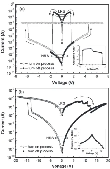
Fig. 3(a) depicts the current–voltage (I–V ) curve of the Al/V:SZO-LNO/Pt device. When a sweep voltage is applied from 0 to +7 or −7 V, the current of the device increases rapidly, and the device is switched from high resistance state (HRS) to low resistance state (LRS), which is defined as the “turn on” process. On the other hand, when a sweep voltage is applied from 0 to +2 or−2 V, the current decreases suddenly and the device is switched from LRS to HRS, defined as the “turn off” process. A current compliance is set at 1 mA during the turn on process to prevent degradation of the device, but
Fig. 2. XRD patterns of LNO films deposited on Pt BE and SiO2layer.
Fig. 3. I–V curves of (a) Al/V:SZO-LNO/Pt device, and (b) Al/V:SZO/LNO
device. The inset is the resistance ratio between two states of each device.
no current compliance is used for the turn off process. The voltage window between turn on and turn off processes is clear enough for accurate switching of the device. The polarity independence on turn on and turn off voltages as shown here
3148 IEEE TRANSACTIONS ON ELECTRON DEVICES, VOL. 54, NO. 12, DECEMBER 2007
is called “nonpolar” switching. Nonpolar switching behavior is proposed in the SZO-based memory device for the first time. The LRS resistance of the device is about 15 Ω, and an equivalent circuit of this device is shown in Fig. 1(a), where the parasitic capacitance is assumed to be ignored. Equation (1) is the series resistance of this device
RV:SZO+ RLNO+ RCPt+ RP = 15 Ω (1) where RV:SZO, RLNO, RCPt, and RPare the sum of the thin film resistance of V:SZO film and contact resistance of Al/V:SZO and V:SZO/LNO interfaces, the sum of the LNO thin film re-sistance and LNO/Pt contact rere-sistance, the crabwise rere-sistance of Pt BE, and other parasitic resistance, respectively. Resistance value of each item shown in (1) is lower than 15 Ω, and the resistivity of platinum is 1.06× 10⁻⁵Ω· cm [21].
The resistance ratio between two states in this device is higher than 107, which is shown in the inset of Fig. 3(a). In addition, a little asymmetric of the I–V curve of the device may be due to the different materials used for BE and TE, which have different work functions and contact resistance with LNO and V:SZO films, respectively.
Fig. 3(b) shows the I–V curve of the Al/V:SZO/LNO device. When a sweep voltage is applied from 0 to−19 V, the device is turned on at about−13 V; when a sweep voltage is applied from 0 to +19 V, the device is turned off after passing through a transition region [13]. The polarity dependence on applying voltages as shown here is called “bipolar” switching. The LRS resistance of the device is about 15 kΩ, and an equivalent circuit of the device is shown in Fig. 1(b) (parasitic capacitance assumed to be ignored). Equation (2) is the series resistance of this device
RV:SZO+ RCLNO+ RP = 15 kΩ (2) where RV:SZO, RCLNO, and RP are the sum of the thin film re-sistance of V:SZO film and contact rere-sistance of Al/V:SZO and V:SZO/LNO interfaces, the crabwise resistance of LNO BE, and other parasitic resistance, respectively. The resistance ratio between the two states in this device is higher than 104, shown in the inset of Fig. 3(b). However, the resistance ratio of this device is three orders of magnitude lower than that of the Al/V:SZO-LNO/Pt device owing to the difference between the LRS resistance of two devices. From (1) and (2), it can be easily understood that the crabwise resistance of LNO BE of the Al/V:SZO/LNO device mainly contributes to the LRS resis-tance, which is similar to a compliance effect although the re-sistance of V:SZO films and parasitic rere-sistance of two devices may have some differences under the distinct turn on processes. Consequently, the device structure of Al/V:SZO-LNO/Pt with lower resistive switching voltage and higher resistance ratio is more suitable for practical NVM applications. However, if the SZO film is directly deposited on Pt or other metals, such as Al, Ti, Ta, Zr, Ni, and Nb, no (100)-preferred orientation film can be obtained, and no good resistive switching behavior can be observed [12]. Therefore, the LNO buffer layer is needed for a SZO-based device with good switching properties. Besides, to prove that the resistive switching does not occur in the LNO film, the resistive switching property was determined between
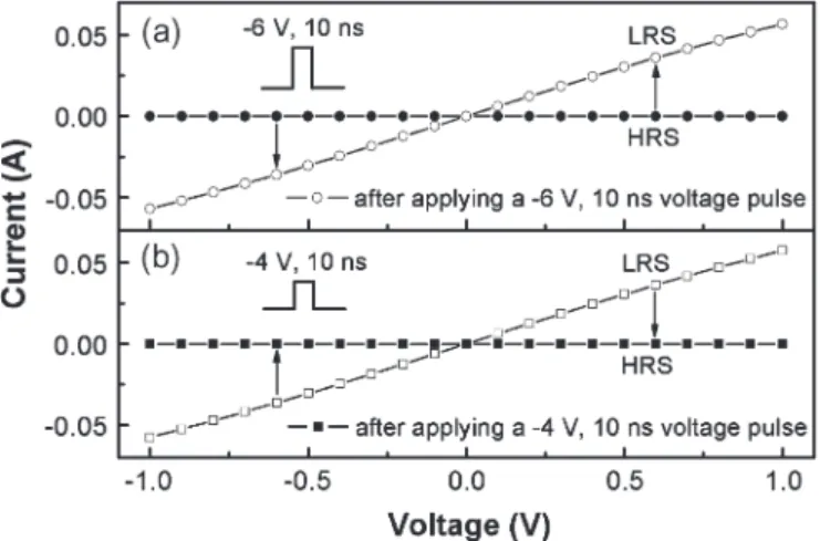
Fig. 4. Resistive switching speed of the Al/V:SZO-LNO/Pt device.
Pt BE and LNO film [Fig. 1(a)], and no resistive switching behavior was observed. Hence, the resistive switching occur-ring in the LNO film can be eliminated. In addition, it was indicated in Fig. 2 that the LNO film quality on Pt is better than that on SiO2, which may be one of the minor reasons for
the aforementioned distinct resistive switching behavior. The voltage polarity of resistive switching will be further discussed in the last paragraph of this section.
Fig. 4 indicates the resistive switching speed of the Al/V:SZO-LNO/Pt device. Fig. 4(a) shows the I–V curves of the device before and after applying a−6 V, 10 ns voltage pulse, and the device is switched from HRS to LRS. On the other hand, this device is switched back to HRS after applying a−4 V, 10 ns voltage pulse shown in Fig. 4(b). The switching speed of turn on and turn off processes is 10 ns. Liu et al. [11] have reported that the device with Al/Cr-doped SZO (Cr:SZO)/LNO structure can be turned on and turned off by applying−20 V, 5 ns and +20 V, 500 µs voltage pulses, respectively. Obviously, the switching speeds between turn on and turn off processes have a difference of five orders of magnitude. The asymmetry of switching speed can be explained by the LNO compliance effect. In the turn off process, electrons are injected from BE to resistive layer, so the conductivity of BE will determine the switching speed of the device. Therefore, the SZO-based memory device using Pt BE can significantly improve the switching speed. In this paper, the Al/V:SZO-LNO/Pt device with high-speed resistive switching of 10 ns is proposed. It is the fastest speed in comparison with those reported in the earlier studies [9], [11], [12].
Fig. 5(a) depicts the plots of Ln(|I|) versus Ln(|V |) of both LRS and HRS currents for the Al/V:SZO-LNO/Pt device. The slopes of LRS curves are close to unity, indicating that the LRS currents are dominated by Ohmic conduction, which is related to thermally excited electrons hopping from one isolated state to the next [22]. On the other hand, the HRS curves are not straight lines, implying that the HRS currents are dominated by other conduction mechanisms. Fig. 5(b) shows the plots of Ln(|I/V |) as a function of |V |1/2 of both HRS and LRS currents for this device. The linear fittings of the device indicate that the HRS currents follow the Frenkel–Poole (F–P) emission, which is corresponding to field-enhanced thermal excitation of trapped electrons into the conduction band [22]. These
Fig. 5. Fitting curves of LRS and HRS currents of the Al/V:SZO-LNO/Pt device by (a) Ohmic conduction, and (b) F–P emission.
results conform to that proposed earlier [13], which implies that the resistive switching mechanisms can be considered as formation and disruption of local conducting paths. Besides, both Ohmic behavior and F–P emission are bulk conduction so that the resistive switching occurring at the interface can be eliminated.
Fig. 6(a) indicates the nondestructive readout property of the Al/V:SZO-LNO/Pt device. The currents of LRSs and HRSs switched by both sweep voltages and voltage pulses remain al-most constant after applying−0.5 V, ongoing bias voltages for more than 104s, which indicates that two resistance states will not be varied after performing 1012 of read pulses (assuming that a read pulse is−0.5 V, 10 ns). Because a sweep voltage can be looked on as a voltage pulse with infinite duration [8], the LRS/HRS current switched by a sweep voltage is higher/lower than that by a voltage pulse, and hence, the resistance ratio between two states switched by sweep voltages is higher than that by voltage pulses. Fig. 6(b) shows the retention time of the Al/V:SZO-LNO/Pt device measured at−0.5 V, indicating that the retention time is longer than 106s and the resistance ratio between two states remains higher than 107. Fig. 6(c) indicates the endurance of the Al/V:SZO-LNO/Pt device measured at −0.5 V, showing that the device can be switched between HRS and LRS for more than 50 times. In summary, the Al/V: SZO-LNO/Pt device with superior resistive switching proper-ties, such as low operating voltage, high operating speed, and
Fig. 6. (a) Nondestructive readout property, (b) Retention time, and (c) Endurance of the Al/V:SZO-LNO/Pt device measured at room temperature.
long retention time, is a possible candidate for next-generation NVM applications.
Table I shows the resistive switching properties of SZO-, TiO2-, and PCMO-based memory devices reported by several
well-known research groups. Based on the experimental results shown in Fig. 3(a), the SZO-based memory device is nonpolar switching, which is different from bipolar switching results
3150 IEEE TRANSACTIONS ON ELECTRON DEVICES, VOL. 54, NO. 12, DECEMBER 2007
TABLE I
DEVICESTRUCTURES, DEPOSITIONMETHOD OFRESISTIVELAYER, RESISTIVESWITCHINGPOLARITIES,ANDSWITCHINGVOLTAGES OFSZO-, TiO2-,ANDPCMO-BASEDMEMORYDEVICESPROPOSED BYSEVERALWELL-KNOWNRESEARCHGROUPS
reported in the earlier studies [9], [10]. Besides, in those studies, the polarities of turn on and turn off voltages are entirely opposite; Beck et al. [9] proposed that their device with Au/Cr : SZO/SrRuO3(SRO) structure could be turned on/off by
apply-ing a negative/positive voltage; nevertheless, Park et al. [10] reported that Pt/Cr:SZO/SRO device could be turned on/off by applying a positive/negative voltage. The different switching properties between these two studies might be due to their different TEs used. Therefore, these results indicate that the electrode materials employed in the device determine its bipolar or nonpolar switching, and the polarity of bipolar switching. In Fig. 3(b), for instance, when the device is turned on, electrons are injected from Al TE into the V:SZO film; whereas in the turn off process, electrons flow from LNO BE into the V:SZO film slowly and trapped by defects uniformly [13]. However, the device cannot be turned on by applying a positive voltage because electrons injected from LNO BE are trapped by defects existing in the V:SZO film and cannot flow to Al TE. Therefore, the distinct resistive switching properties of two devices shown in Fig. 3(a) and (b) are due to different BEs used, that is, the dis-tinct switching is attributed to different conductivities between Pt and LNO BEs. Similar results are also observed in TiO2- and
PCMO-based memory devices. In TiO2-based memory
de-vices, Fujimoto et al. [15] proposed bipolar switching of the Pt/TiO2/TiN device; however, Choi et al. [16] reported
non-polar switching of the Pt/TiO2/Ru device. In PCMO-based
memory devices, Sawa et al. [6] reported bipolar switching of the Ti/PCMO/SRO device, while Fujimoto et al. [7] reported nonpolar switching of the Pt/PCMO/Pt device. Consequently, nonpolar switching is considered as an intrinsic property of SZO-, TiO2-, and PCMO-based memory devices; however, the
electrode materials employed, which have different conduc-tivities, would dominate their bipolar or nonpolar switching behavior and the polarity of bipolar switching. Therefore, ap-propriate electrode materials chosen are indeed important for obtaining an RRAM device with excellent properties. However, other factors, such as work function of electrodes, contact resistance between two films, microstructure of resistive layer, and work function difference and property of each interface,
still need further detailed studies for developing an excellent RRAM device.
IV. CONCLUSION
The experimental results reported in this paper indicate that the electrode materials with different conductivities sig-nificantly affect the resistive switching properties of the de-vices. The device with Al/V:SZO-LNO/Pt structure shows nonpolar switching property, whereas the Al/V:SZO/LNO de-vice depicts bipolar switching behavior. The resistance ratios between two states are 107 and 104 for Al/V:SZO-LNO/Pt and Al/V:SZO/LNO devices, respectively, which is due to the resistance difference between the LRS of two devices. The device with Pt BE has lower switching voltages and higher resistance ratio, while the device with LNO BE possesses higher switching voltages and lower resistance ratio. Such a different behavior is attributed to a high resistance of LNO BE in comparison with a low resistance of Pt BE. The switching speed of the Al/V:SZO-LNO/Pt device is 10 ns, which is the fastest speed in comparison with those of the earlier mentioned reports. The conduction mechanisms of LRS and HRS currents are Ohmic and F–P behavior, respectively, which is consid-ered as formation and disruption of local conducting paths in the resistive layer. The nondestructive readout property of the Al/V:SZO-LNO/Pt device is demonstrated, and the retention time of the device longer than 106 s is also performed in this paper. Therefore, the Al/V:SZO-LNO/Pt memory device, having good switching properties, is a possible candidate for next-generation NVM applications.
REFERENCES
[1] W. W. Zhuang, W. Pan, B. D. Ulrich, J. J. Lee, L. Stecker, A. Burmaster, D. R. Evans, S. T. Hsu, M. Tajiri, A. Shimaoka, K. Inoue, T. Naka, N. Awaya, K. Sakiyama, Y. Wang, S. Q. Liu, N. J. Wu, and A. Ignatiev, “Novell colossal magnetoresistive thin film nonvolatile resistance random access memory (RRAM),” in IEDM Tech. Dig., 2002, pp. 193–196. [2] A. Chen, S. Haddad, Y.-C. Wu, T.-N. Fang, Z. Lan, S. Avanzino,
S. Pangrle, M. Buynoski, M. Rathor, W. Cai, N. Tripsas, C. Bill, M. VanBuskirk, and M. Taguchi, “Non-volatile resistive switching for advanced memory applications,” in IEDM Tech. Dig., 2005, pp. 746–749.
[3] I. G. Baek, M. S. Lee, S. Seo, M. J. Lee, D. H. Seo, D.-S. Suh, J. C. Park, S. O. Park, H. S. Kim, I. K. Yoo, U.-I. Chung, and J. T. Moon, “Highly scalable non-volatile resistive memory using simple binary oxide driven by asymmetric unipolar voltage pulses,” in IEDM Tech. Dig., 2004, pp. 587–590.
[4] I. G. Baek, D. C. Kim, M. J. Lee, H.-J. Kim, E. K. Yim, M. S. Lee, J. E. Lee, S. E. Ahn, S. Seo, J. H. Lee, J. C. Park, Y. K. Cha, S. O. Park, H. S. Kim, I. K. Yoo, U.-I. Chung, J. T. Moon, and B. I. Ryu, “Multi-layer cross-point binary oxide resistive memory (OxRRAM) for post-NANDstorage application,” in IEDM Tech. Dig., 2005, pp. 750–753. [5] H. Sim, H. Choi, D. Lee, M. Chang, D. Choi, Y. Son, E.-H. Lee, W. Kim, Y. Park, I.-K. Yoo, and H. Hwang, “Excellent resistance switching characteristics of Pt/SrTiO3 Schottky junction for
multi-bit nonvolatile memory application,” in IEDM Tech. Dig., 2005, pp. 758–761.
[6] A. Sawa, T. Fujii, M. Kawasaki, and Y. Tokura, “Hysteretic current– voltage characteristics and resistance switching at a rectifying Ti/ Pr0.7Ca0.3MnO3interface,” Appl. Phys. Lett., vol. 85, no. 18, pp. 4073–
4075, Nov. 2004.
[7] M. Fujimoto, H. Koyama, S. Kobayashi, Y. Tamai, N. Awaya, Y. Nishi, and T. Suzuki, “Resistivity and resistive switching properties of Pr0.7Ca0.3MnO3thin films,” Appl. Phys. Lett., vol. 89, no. 24, p. 243 504,
Dec. 2006.
[8] A. Sawa, T. Fujii, M. Kawasaki, and Y. Tokura, “Interface resistance switching at a few nanometer thick perovskite manganite active layers,”
Appl. Phys. Lett., vol. 88, no. 23, p. 232 112, Jun. 2006.
[9] A. Beck, J. G. Bednorz, C. Gerber, C. Rossel, and D. Widmer, “Repro-ducible switching effect in thin oxide films for memory applications,”
Appl. Phys. Lett., vol. 77, no. 1, pp. 139–141, Jul. 2000.
[10] J.-W. Park, J.-W. Park, M. K. Yang, K. Jung, D.-Y. Kim, and J.-K. Lee, “Low-voltage resistive switching of polycrystalline SrZrO3:Cr thin films
grown on Si substrates by off-axis rf sputtering,” J. Vac. Sci. Technol. A,
Vac. Surf. Films, vol. 24, no. 4, pp. 970–973, Jul. 2006.
[11] C.-Y. Liu, P.-H. Wu, A. Wang, W.-Y. Jang, J.-C. Young, K.-Y. Chiu, and T.-Y. Tseng, “Bistable resistive switching of a sputter-deposited Cr-doped SrZrO3 memory film,” IEEE Electron Device Lett., vol. 26,
no. 6, pp. 351–353, Jun. 2005.
[12] C.-Y. Liu, A. Wang, W.-Y. Jang, and T.-Y. Tseng, “Electrical properties of resistance switching V-doped SrZrO3films on textured LaNiO3
bot-tom electrodes,” J. Phys. D, Appl. Phys., vol. 39, no. 6, pp. 1156–1160, Mar. 2006.
[13] C.-C. Lin, B.-C. Tu, C.-C. Lin, C.-H. Lin, and T.-Y. Tseng, “Resistive switching mechanisms of V-doped SrZrO3memory films,” IEEE Electron
Device Lett., vol. 27, no. 9, pp. 725–727, Sep. 2006.
[14] Y. Watanabe, J. G. Bednorz, A. Bietsch, C. Gerber, D. Widmer, A. Beck, and S. J. Wind, “Current-driven insulator–conductor transition and non-volatile memory in chromium-doped SrTiO3single crystals,” Appl. Phys.
Lett., vol. 78, no. 23, pp. 3738–3740, Jun. 2001.
[15] M. Fujimoto, H. Koyama, M. Konagai, Y. Hosoi, K. Ishihara, S. Ohnishi, and N. Awaya, “TiO2anatase nanolayer on TiN thin film exhibiting
high-speed bipolar resistive switching,” Appl. Phys. Lett., vol. 89, no. 22, p. 223 509, Nov. 2006.
[16] B. J. Choi, D. S. Jeong, S. K. Kim, C. Rohde, S. Choi, J. H. Oh, H. J. Kim, C. S. Hwang, K. Szot, R. Waser, B. Reichenberg, and S. Tiedke, “Resistive switching mechanism of TiO2 thin films grown
by atomic-layer deposition,” J. Appl. Phys., vol. 98, no. 3, p. 033 715, Aug. 2005.
[17] K. Kinoshita, T. Tamura, M. Aoki, Y. Sugiyama, and H. Tanaka, “Bias polarity dependent data retention of resistive random access memory consisting of binary transition metal oxide,” Appl. Phys. Lett., vol. 89, no. 10, p. 103 509, Sep. 2006.
[18] D. C. Kim, S. Seo, S. E. Ahn, D.-S. Suh, M. J. Lee, B.-H. Park, I. K. Yoo, I. G. Baek, H.-J. Kim, E. K. Yim, J. E. Lee, S. O. Park, H. S. Kim, U.-I. Chung, J. T. Moon, and B. I. Ryu, “Electrical obser-vations of filamentary conductions for the resistive memory switching in NiO films,” Appl. Phys. Lett., vol. 88, no. 20, p. 202 102, May 2006. [19] J. He, L. Ma, J. Wu, and Y. Yang, “Three-terminal organic memory
devices,” J. Appl. Phys., vol. 97, no. 6, p. 064 507, Mar. 2005.
[20] Y.-S. Lai, C.-H. Tu, D.-L. Kwong, and J. S. Chen, “Charge-transport characteristics in bistable resistive poly (N-vinylcarbazole) films,” IEEE
Electron Device Lett., vol. 27, no. 6, pp. 451–453, Jun. 2006.
[21] J. P. Schaffer, A. Saxena, S. D. Antolovich, T. H. Sanders, and S. B. Warner, The Science and Design of Engineering Materials. New York: McGraw-Hill, 1999, p. 446.
[22] S. M. Sze, Physics of Semiconductor Device. New York: Wiley, 1981, pp. 402–407.
Chun-Chieh Lin was born in Hualien, Taiwan,
R.O.C., in 1980. He received the B.S. and Ph.D. de-grees in electronics engineering from the Department of Electronics Engineering and Institute of Elec-tronics, National Chiao-Tung University, Hsinchu, Taiwan, R.O.C., in 2002 and 2007, respectively.
He is currently a Postdoctoral Researcher of Na-tional Chiao-Tung University. His research interests include in developing and exploring the resistive random access memory.
Chih-Yang Lin was born in Kaohsiung, Taiwan,
R.O.C., in 1982. He received the B.S. degree from the Department of Electronics Engineering, National Chiao-Tung University, Hsinchu, Taiwan, R.O.C. in 2004. He is currently pursuing the Ph.D. degree from the Institute of Electronics, National Chiao-Tung University.
His current research is the fabrication and analysis of resistive random access memory.
Meng-Han Lin was born in Taichung, Taiwan,
R.O.C., in 1981. He received the B.S. degree in physics from National Central University, Taoyuan, Taiwan, R.O.C., in 2004, and the M.S. degree in electronics engineering from National Chiao-Tung University, Hsinchu, Taiwan, R.O.C., in 2006. He is now pursuing the Ph.D. degree from the Institute of Electronics, National Chiao-Tung University.
His research interests are high dielectric constant materials and resistive random access memory.
Chen-Hsi Lin (M’93) received the Ph.D.
de-gree in applied physics from Harvard University, Cambridge, MA.
He was with Hewlett-Packard IC Processing Lab-oratory, Palo Alto, CA, from 1983 to 1995. He joined Winbond Electronics Corporation, Hsinchu, Taiwan, R.O.C., in 1995 as Director of technology development. His primary interests are advanced CMOS device design, nonvolatile memory, and low power DRAM technologies. He is now Vice Pres-ident of Technology R&D Group, Winbond Elec-tronics Corporation.
Tseung-Yuen Tseng (M’93–SM’94–F’02) received
the Ph.D. degree in electroceramics from the School of Materials Engineering, Purdue University, West Lafayette, IN, in 1982.
He was briefly associated with the University of Florida, Gainesville, before joining National Chiao-Tung University, Hsinchu, Taiwan, R.O.C., in 1983, where he is now a University Chair Professor in the Department of Electronics Engineering and In-stitute of Electronics. His professional interests are electronic ceramics, nanoceramics, ceramic sensors, ferroelectric thin films and their based devices, and resistive switching memory devices. He has published over 300 refereed journal papers and conference pa-pers and held eight patents. He is an Associate Editor of Journal of Nanoscience
and Nanotechnology and Advanced Science Letters.
Dr. Tseng has received Distinguished Research Award (three times) from the National Science Council (1995–2001), Hou Chin-Tui Distinguished Honor Award (2002), Dr. Sun Yat-Sen Academic Award (2003), TECO Technology Award (2004), IEEE CPMT Exceptional Technical Achievement Award (2005), Distinguished Research Award of Pan Wen Yuan Foundation (2006) and Academic Award of Ministry of Education (2006). He was elected a Fellow of the American Ceramic Society in 1998. He is currently the Vice President and University Chair Professor of the National Taipei University of Technology, Taipei, Taiwan, R.O.C.