國 立 交 通 大 學
電子工程學系 電子研究所碩士班
碩 士 論 文
具有昇起式源/汲極之多晶鍺薄膜電晶體的
元件製作與特性分析
A Study of the Fabrication and Characteristics
of Poly-Ge Thin-Film Transistors
with Raised Source/Drain
研 究 生:陳冠宇
指導教授:林鴻志 博士
黃調元 博士
具有昇起式源/汲極之多晶鍺薄膜電晶體的
元件製作與特性分析
A Study of the Fabrication and Characteristics
of Poly-Ge Thin-Film Transistors
with Raised Source/Drain
研 究 生:陳冠宇 Student:Kuan-Yu Chen
指導教授:林鴻志 博士 Advisors:Dr. Horng-Chih Lin
黃調元 博士 Dr. Tiao-Yuan Huang
國 立 交 通 大 學
電子工程學系 電子研究所碩士班
碩 士 論 文
A Thesis
Submitted to Department of Electronics Engineering & Institute of Electronics College of Electrical and Computer Engineering
National Chiao-Tung University in Partial Fulfillment of the Requirements
for the Degree of Master of Science
in
Electronic Engineering September 2010
Hsinchu, Taiwan, Republic of China
i
具有昇起式源/汲極之多晶鍺薄膜電晶體的
元件製作與特性分析
研究生 : 陳冠宇 指導教授 : 林鴻志 博士
黃調元 博士
國立交通大學
電子工程學系 電子研究所碩士班
摘要
在本篇論文中,我們製作並探討含有矽化鎳或多晶矽之昇起式源/汲極的多 晶鍺電晶體特性。在製作元件過程中,利用低溫500℃的固相結晶法形成多晶鍺 通道。而由於缺陷出現於元件氧化層與通道的介面之間,因此初完成的元件特性 尚未能穩定。但在經過多次的量測之後,元件表現出較好的次臨界擺幅特性(subthreshold swing),並達到等級約為105的開關電流比(Ion/Ioff ratio)。然而,透過
固相結晶法形成的多晶鍺,其晶粒尺寸偏小,使得臨界電壓的範圍廣且差異幅度 從7.75V至10.75V。
另外,我們認為昇起式源/汲極區域的鎳化矽與多晶矽於固相結晶時為多晶 鍺通道的種晶層(seeding layer)。進一步萃取昇起式多晶矽與鎳化矽源/汲極區域
ii
的電阻值,分別為0.575MΩ與0.490 MΩ。除此之外,由於種晶層對非晶鍺的結晶 影響,多晶鍺通道的結晶度為非均勻並與所處的位置相關。
最後,我們討論不同的汲極對源極的電壓對電流電壓特性。即使在通道較長 的尺寸下,我們發現汲極引致晶粒能障下降(drain–induced grain barrier lowering, DIGBL)效應應為在不同的汲-源電壓下導致電流變化的主要原因。
iii
A Study of the Fabrication and Characteristics
of Poly-Ge Thin-Film Transistors
with Raised Source/Drain
Student : Kuan-Yu Chen Advisors : Dr. Horng-Chih Lin
Dr. Tiao-Yuan Huang
Department of Electronics Engineering and Institute of Electronics
National Chiao Tung University, Hsinchu, Taiwan
Abstract
In this thesis, we have fabricated and characterized poly-Ge TFT devices with
raised NiSi or poly-Si source/drain (S/D). The poly-Ge channel was formed with
solid-phase crystallization (SPC) method at a lower temperature (500℃). The fresh
device characteristics are not stable due to the defects presenting at or near the
channel/oxide interface. After several repeated measurements are executed, superior
device performance with smaller S.S. and Ion/Ioff ratio of about 105 is achieved.
However, owing to the small grain size formed by SPC treatment, the threshold
iv
The poly-Si and NiSi are expected to serve as the seeding layer for
crystallization during the SPC treatment. Furthermore, we also extracted the RSD for
raised poly-Si and NiSi S/D and found to be 0.575 MΩ and 0.490 MΩ, respectively.
Moreover, we also showed that the crystallinity in the channel is non-uniform and
location dependent, owing to the action of the seeding layer in crystallizing the α-Ge.
Finally, the ID-VG characteristics under different VDS also have been investigated.
Even when the channel length is long, we also found that the DIGBL effect is likely the main cause for the significant shift in ID as VDS is varied.
v
Acknowledgment
兩年的碩士生涯過去了,開始要寫這頁的同時,過去的點點滴滴皆浮現於腦 海中,當然能夠完成這本論文要感謝的人非常多。首先,我要感謝我的指導教授 林鴻志博士和黃調元博士。感謝林鴻志老師總能準確的指出任何事情的癥結所在, 無論是在實驗操作、元件物理亦或是研究態度,也感謝黃調元老師教導我待人接 物的道理,從兩位老師的教導之中學到了何謂”學然後知不足”。 接著,要感謝國家奈米實驗室的陳仕鴻博士,給我許多專業知識以及研究上 的幫助。而這兩年當中,最要感謝的就是陳威臣學長了,不厭其煩的帶著我做實 驗以及不斷的提供我研究中的想法,讓我的經驗累積從無到有;也因為學長,啟 發了我對英文的學習熱情。感謝哲民、蘇博、徐博、子儀、MACA、阿毛學長, 於實驗上我所遭遇的問題幾乎都可迎刃而解。另外要感謝張佑寧學長,教導我鍺 元件的製作與實驗上的幫助。 感謝簡博於實驗及修課中的支援,使得你那俊俏的cos照更加帥氣;感謝家 維兄,總在我最難過時伸出援手,我不會忘記馬偕的那個夜晚;感謝正瑋兄,不 管出會幾秒就合體,永遠會記得你的義氣與貼心;感謝pH值稍低的小輔神,因 為有你實驗室氣氛更加的熱絡;感謝距離頂級廚師只差一步的劉媽媽,出遊或是 聚會總能完美的開始至結束;感謝阿智,於修課的期間大力的幫忙。謝謝你們, 毫無血緣的大家能夠相聚一起,使得這兩年的記憶更加的完整,最不會忘記的就 是對我所喊的一聲”兄弟”。感謝姚明陪伴我度過最辛苦的一年,以及感謝和苑的 大家,むむ先生、企鵝、達哥、たくみ先生、阿部先生、馥霓老師在我碩士的生 涯的最後三個月給我無限的活力及勇氣。 最後,感謝我最愛的家人,感謝爸爸、媽媽、姊姊在我背後默默的支持著我, 才能讓我於求學的路上順利至此,親情的羈絆永遠是我前進的動力。謝謝N。 陳冠宇 致於風城交大 2010年9月vi
Contents
Abstract (Chinese)………... i
Abstract (English)………... iii
Acknowledgment (Chinese) ………... v
Contents ………... vi
Figure Captions………... viii
Table Captions ……….... xi
Chapter 1 Introduction………...
11-1 Overview………. 1
1-2 Motivation.……….. 7
1-3 Thesis Organization...………. 8
Chapter 2 Device Structure, Fabrication and Measurement Setups…..
102-1 Device Structure and Process Flow...…...………. 10
2-1-1 TFT Devices with Raised Poly-Si S/D……… 10
2-1-2 TFT Devices with Raised NiSi S/D………. 12
2-2 Measurement Setup for Electrical Characterization……….……... 13
Chapter 3 Electrical Characteristics of Raised S/D Poly-Ge TFTs……
163-1 Basic Electrical Characteristics of Raised S/D Poly-Ge TFTs……...……… 16
3-1-1 Transfer Characteristics………..………. 17
vii
3-2 Series Resistance and Effective Channel Length…….………... 21
3-3 Drain Induced Grain Barrier Lowering Effect……… 24
3-4 Comparisons among Different Poly-Ge TFT Devices……… 27
Chapter 4 Conclusion and Future Work………...
314-1 Summary and Conclusion………...……… 31
4-2 Future Work……… 32 References ……… Figures………... 34 42 Vita……… 68
viii
Figure Captions
Chapter 1Chapter 2
Fig. 2-1. (a) Top view layout of a raised S/D TFT device. (b) Cross-section view of a TFT device with raised poly-Si S/D. (c) Cross-section view of a TFT device with raised NiSi S/D. (d) SEM picture of a TFT device with raised NiSi S/D………...42 Fig. 2-2. Process flow of the TFT device with raised poly-Si S/D...43 Fig. 2-3. Process flow of the TFT device with raised NiSi S/D ...44
Chapter 3
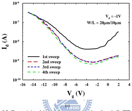
Fig. 3-1. Transfer curves of two different poly-Ge TFT devices [30]...45 Fig. 3-2. Characteristics of drain current versus gate voltage for poly-Ge TFTs with raised poly-Si S/D showing gradually stabilized characteristics with increasing measurement sequence. (a)L=2 μm. (b)L=5 μm. (c)L=10 μm...47 Fig. 3-3. Characteristics of drain current versus gate voltage for poly-Ge TFTs with
raised NiSi S/D showing gradually stabilized characteristics with increasing measurement sequence. (a)L=2 μm. (b)L=5 μm. (c)L=10 μm...49 Fig. 3-4. Fig. 3-4. TEM cross-sectional view of poly-Ge film annealed at 500℃ for 1
hour. [30]...50 Fig. 3-5. Id-Vg curves as a function of channel length for poly-Ge TFTs with (a)
raised poly-Si S/D and (b) raised NiSi S/D...51 Fig. 3-6. SS versus channel length for poly-Ge TFTs with (a) raised poly-Si S/D and
ix
(b) raised NiSi S/D...52 Fig. 3-7. Threshold voltage distribution with raised S/D made of (a) Poly-Si. (b)
NiSi...53 Fig. 3-8. Threshold voltage versus channel length for poly-Ge TFTs with raised poly-Si S/D and raised NiSi S/D...54 Fig. 3-9. Mobility versus channel length for poly-Ge TFTs with (a) raised poly-Si
S/D and (b) raised NiSi S/D...55 Fig. 3-10. (a) Schematic picture indicating the route of current flow at the source/drain
side. (b) Components of parasitic source/drain series resistance...56 Fig. 3-11. Output characteristics of poly-Ge TFTs with (a) raised poly-Si S/D and (b)
raised NiSi S/D...57 Fig. 3-12. (a) Equivalent circuit of TFT with source and drain resistance [42]. (b) Equivalent circuit of TFT with re-defined terminal voltages...58 Fig. 3-13. Extraction of RSD and Leff of poly-Ge TFT with raised poly-Si S/D. (a) Rm
verse L. (b) B versus A...59 Fig. 3-14. Extraction of RSD and Leff of poly-Ge TFT with raised NiSi S/D. (a) Rm
verse L. (b) B versus A...60 Fig. 3-15. Schematic view of crystallized Ge channel with raised S/D as seeding layer. Section 1 indicates the regions with better crystallinity than Section 2...61 Fig. 3-16. Id-Vg curves measured under various drain bias for poly-Ge TFTs with
poly-Si raised S/D region. (a) L = 5 μm. (b) L = 10 μm...62 Fig. 3-17. Id-Vg curves measured under various drain bias for poly-Ge TFTs with NiSi
raised S/D region. (a) L = 5 μm. (b) L = 10 μm...63 Fig. 3-18. Cross-sectional view of an n-type polycrystalline TFT and the potential
x
Fig. 3-19. Energy-level diagram for a grain boundary under a lateral bias ΔV in an n-type polycrystalline film [45]...64 Fig. 3-20. (a) Process flow and schematic cross section [46] and (b) transfer characteristics of NiGe Schottky S/D poly-Ge TFT [47]...65 Fig. 3-21. (a) Process flow and schematic cross section and (b) transfer characteristics of the single-crystalline Ge p-channel TFT on polyimide substrate [48]...66 Fig. 3-22. Process flow and schematic cross section of poly-Ge on poly-Si film p-channel TFT [30]...67
xi
Table Captions
Table. 1-1. Material characteristics of alternative channel materials [1]……...……..9
Table. 2-1. Split conditions of the raised S/D structures………...15
Table. 3-1. Major characteristics of poly-Ge TFT devices………...30
Table. 3-2. Corrected mobility by taking into account RSD effect...30
1
Chapter 1
Introduction
1-1 Overview
Early in 1947, Bardeen and Brattain in Bell lab invented the first contact point
transistor using germanium (Ge) accidentally. This important breakthrough opened
the gate to the semiconductor industry nowadays. Ge had been the main material for
the development of bipolar transistors, while its progress in field-effect devices was
less prosperous, because of the low quality of its native oxide (GeO2) [1], which
cannot provide sufficient passivation of the surface. Moreover, the thermal stability of
formed GeO2 is inferior to SiO2 and is soluble in water, so the Ge oxide layer will
easily degrade in the process of fabrication. Owing to the relatively much cheaper
material cost of Si, as well as the intriguing properties of the silicon dioxide (SiO2),
such as excellent stability in water, effective passvation of the Si surface, higher
mechanical strength, and better heat conductivity, Si-based
metal-oxide-semiconductor (MOS) transistors succeeded bipolar transistors as the
major active device in chips in 1960s. Si has been the mainstream substrate of
2
In 1965 Gordon Moore predicted that the number of transistors per integrated
circuit would double every 12 months. Although the period he predicted is not so
accurate (practical period is around 18 months), the trend he recognized is still
profound and continues to this date. To maintain Moore‟s Law, the semiconductor
industry keeps shrinking the dimensions of the transistors with improved performance.
Indeed, the trend in reducing feature sizes enables higher operation speed, lower
operation voltage, and reduced cost per transistor. However, at the 32 nm technology
node and beyond, the scaling methodology for conventional planar transistors
encounters technological problems and fundamental challenges [2]. Some issues arise
due to dimension scaling, like high leakage with ultra-thin gate oxide and very
shallow source/drain (S/D) junctions, and mobility degradation due to the use of
heavy substrate doping for suppression of subthreshold leakage and short-channel
effects. Actually these issues are difficult to overcome for achieving the targets of
device performance requested by International Technology Roadmap for
Semiconductors (ITRS) roadmap [3].
To address those issues, it may need to bring new materials and structures into
the manufacturing. For examples, high-k material for replacing silicon dioxide as the
gate dielectric and new semiconductor layers with high carrier mobility for replacing
3
has been regarded as one of the appropriate candidates for future CMOS technology
due to its 2x higher intrinsic electron mobility and 4x higher intrinsic hole mobility
over Si [1]. Moreover, the bulk hole mobility of Ge is the highest among group IV and
III-V semiconductor materials as shown in Table 1.1 [1]. Because of its low melting
point (937 ℃ for crystal Ge), Ge-based devices are usually processed at temperatures
much lower than that for Si counterparts. For example, the source/drain dopant
activation can be done at a temperature ranging from 400 to 500 ℃. Such low
temperature helps control the impurity profile suitable for forming shallow junctions
for better control of short-channel effects. Therefore, Ge is highly suitable for
three-dimensional integrated circuits (3D-ICs) which request low-temperature
fabrication [5], [6]. For thin-film transistors (TFTs), the low temperature processing
also benefits the use of low-cost substrates.
However, to realize the advantages as mentioned above, a lot of pending issues
need to be addressed and solved. First, Ge has a smaller bandgap, Eg, as compared
with Si. Although this property allows a lower power supply voltage, VDD, to be used
in Ge-based devices and circuits, the smaller bandgap could also result in significant
increase in junction leakage. Additionally, there exist many defects at the interface
between Ge and the gate dielectric layer which deteriorate the subthrehold swing (SS)
4
solubility of n-type dopants in Ge is low while the dopants diffusion speed is quite
fast [7], so high-performance n-type devices are hard to fabricate. Furthermore, as
compared with Si, the natural reserve of Ge on earth is scarce. Thus, unlike the Si
wafers, the supply of bulk Ge wafers definitely can not sustain the industrial demand.
However, taking the advantage of the high mobility in Ge, some studies have
demonstrated high-mobility bulk Ge p-FETs with different gate dielectric including
HfO2, Al2O3, and GeON [8]-[11]. Experimental results showed that the fabricated
devices can exhibit about >1.5x hole-mobility enhancement as compared with
conventional Si p-MOSFETs. In addition, Schottky-barrier S/D Ge p-channel
MOSFETs were proposed to reduce the series resistance. The drain drivability is
improved over the Si counterpart due to the lower Schottky barrier height of holes at
the germanide-Ge contact as well as the higher mobility of Ge channel [12]. Recently,
Ge-based p-MOSFETs have been successfully formed on thin Ge layer epitaxially
grown on Si substrate. To overcome the issue of large S/D resistance in thin body
structures, Schottky barrier S/D GOI MOSFETs were proposed and implemented
[13]-[17].
Furthermore, Ge/Si and SiGe/Si heterostructures have been used in
high-performance devices because of their higher electron and hole mobilities
5
achieving higher MOSFET performance with lower leakage current as well as
high-speed operation. However, for thin film transistor (TFT) applications, some
studies have demonstrated the fabrication of Ge thin films deposited on SiO2-covered
Si substrates at a low temperature around 350 ℃ using chemical vapor deposition
(CVD) techniques [18], yet there are rare studies about the deposition of Ge film by
physical vapor deposition (PVD) technique. By low-pressure CVD (LPCVD) using
GeH4 as the reaction gas, before the growth of Ge film, an incubation time was
usually found, during which Ge nuclei were formed on Si [18]. Besides, the nucleus
size would vary depending on some factors such as the type of carrier gas. Using
high-density plasma CVD (HDP-CVD) system, pure and high-quality Ge film have
been deposited with nearly no incubation time using a mixture of GeH4/H2 as process
gas at 400 ℃. The cubic structure with primarily (111) orientation of the Ge films is
mainly composed of fine grains [19]. Through inductively coupled plasma CVD
(ICP-CVD) system, polycrystalline Ge (poly-Ge) films can be directly deposited onto
a SiO2-covered Si substrate at a relatively low temperature and exhibit the same cubic
structures. Although the characteristics of the low-temperature deposited Ge film are
slightly worse, subsequent annealing can improve the crystalline quality significantly
[20].
6
for realization of advanced system-on-panel (SOP) applications. Moreover, the
process temperature of poly-Ge can be reduced and easily implemented on the glass
substrate. There are several methods for the fabrication of poly-Ge, especially from
amorphous Ge (α-Ge) to poly-Ge, including solid-phase crystallization (SPC) [21],
liquid-phase epitaxy (LPE) [22], metal-induced crystallization (MIC) [6], [23], [24],
metal-induced lateral crystallization (MILC) [25] and so on.
Similar to the fabrication of poly-Si film for TFT applications, SPC is also a
common technique to transform α-Ge to poly-Ge. The SPC mechanism is interpreted
as a bond rearrangement process at the interface of the amorphous layer and the
crystalline layer, α-Si/poly-Si or α-Ge/poly-Ge. In the interface, the bond breaking is
thermally activated at the defect sites [21]. At first the crystalline film can
heterogeneously nucleate at the defect sites or the interfaces serving as the nucleation
centers or homogeneously nucleate within the amorphous film. The grains gradually
enlarge until the two adjoining grains merge and forms a region called the grain
boundary.
The activation energy of SPC is given by the sum of the maximum distortion
energy encountered during the migration of dangling bond and the broken energy of
the bond. However, the average grain size of poly-Ge formed by SPC is relatively
7
would encounter serious scattering from the grain boundaries. And there are more
grain boundaries in poly-Ge, where abundant intra-grain strain bonds and dangling
bonds exist, and are more likely to trap carriers. Not only would the carrier mobility
be degraded, the performance of devices would also be significantly influenced. In
light of this, several approaches for enlarging the grain size have been proposed and
investigated, such as two-step SPC [27].
Also, with low melting point, Ge is appropriate for three dimensional integrated
circuits (3D-ICs) which required low process temperature. Monolithic 3D-ICs employ
a bottom-up manufacturing of 3D layers and the 3D structure provides the potential
for the shorter length (vertical) of interconnectivity [25]. In order to conserve
underlying layers, it requires low processing temperature, hence, the fabrication is
challenging. Moreover, there still exist some issues for use of Ge in device-level
applications.
1-2 Motivation
Taking advantage of Ge‟s higher hole and electron mobilities in low electric
fields, and lower manufacturing temperature over Si as mentioned earlier in this
chapter, Ge devices have been proposed as the candidate beyond the scaling limit of
8
Ge-MOSFETs fabricated on bulk Ge and Ge-on-insulator (GOI). For TFT
applications, some studies have discussed the deposition of α-Ge or poly-Ge film by
CVD technique which is done at a higher temperature than PVD technique. However,
the deposition of Ge film by physical vapor deposition (PVD) method is rarely
explored. Besides, in order to reduce the S/D resistance, the raised S/D (RSD) structure
is adopted. Therefore, with low-temperature fabrication (<500 ℃), the purpose of
this study is to investigate and characterize poly-Ge devices with various structures
fabricated with Ge films deposited with an ultrahigh vacuum (UHV) sputtering
system.
1-3 Thesis Organization
The organization of this thesis is divided into four chapters. A brief overview and
motivation are given in this chapter. In Chapter 2, we briefly describe the device
structures and process flow for fabricating the structures of poly-Ge devices with
raised source/drain (S/D) region. In Chapter 3, the electrical characteristics of devices
and phenomenon in these poly-Ge devices are investigated and discussed. Finally, a
summary of conclusion achieved in this thesis and suggestions for future work are
9 Table 1-1
Material characteristics of alternative channel materials [1].
Ge Si GaAs InSb InP
Bandgap,Eg (ev) 0.66 1.12 1.42 0.17 1.35
Electron affinity, χ (ev) 4.05 4.0 4.07 4.59 4.38
Hole mobility, μh (cm2V-1s-1) 1900 450 400 1250 150
Electron mobility, μe (cm2V-1s-1) 3900 1500 8500 80000 4600
Dielectric constant, κ 16.0 11.9 13.1 17.7 12.4
10
Chapter 2
Device Structure, Fabrication and
Measurement Setups
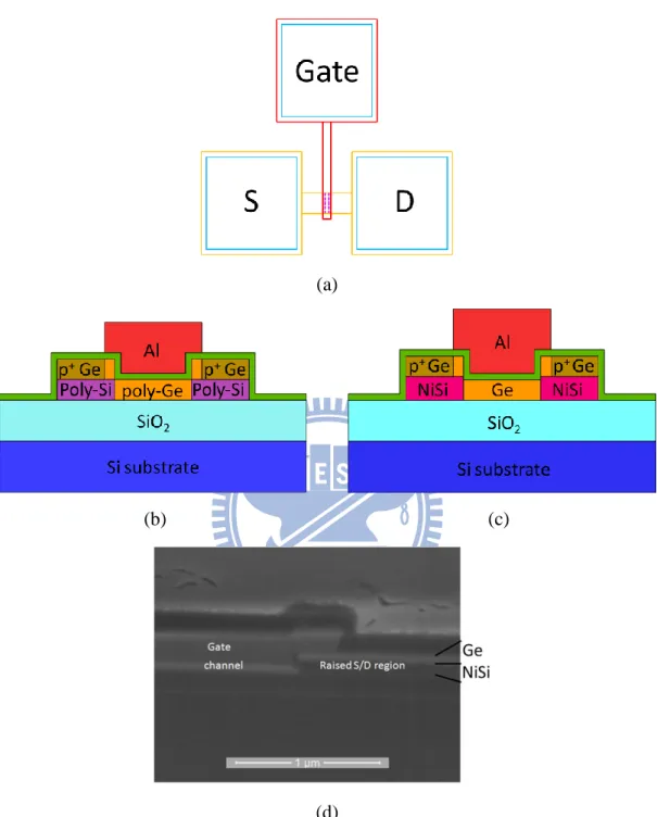
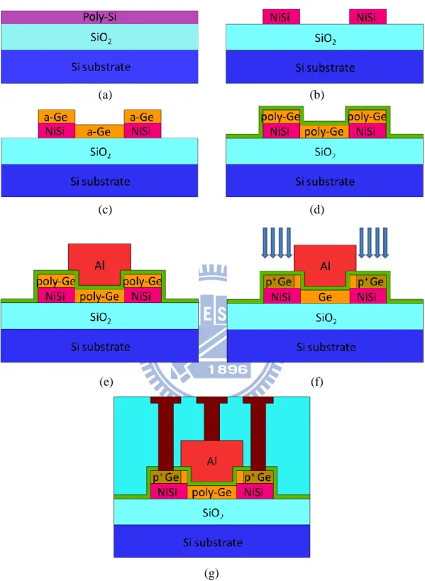
2-1 Device Structure and Process Flow
In this chapter, we describe the fabrication process in detail for TFTs with raised
S/D. The top and cross-sectional views of the device structure are illustrated in Fig.
2-1, while Fig. 2-2 and Fig. 2-3 depict the process flow to fabricate the two types of
raised S/D structure adopted in the study, namely, raised poly-Si S/D and
nickel-silicide (NiSi) S/D. The incentive of employing these structures is to reduce the
parasitic S/D resistance and to study their impacts on the device characteristics.
Subsequently, the measurement setups for electrical characterization are presented.
2-1-1 TFT Devices with Raised Poly-Si S/D
Figure 2-1 (a) is the top-view of the fabricated device. The cross-sectional view
of the device with raised poly-Si S/D and the process steps for the fabrication of the
devices are illustrated in Fig. 2-1 (b) and Figs. 2-2 (a)~(f), respectively. First, 6-inch
11
thick-poly-Si by furnace and LPCVD systems, respectively, were used as the starting
substrates, as shown in Fig. 2-2 (a). After the poly-Si layer was formed, BF2+ ion
implantation was carried out at 20 keV with a dose of 5x1015 cm-2. Then, dopant
activation was performed at 600 ℃ for 12 hours in nitrogen ambient. Afterwards,
I-line lithography was used to pattern the raised S/D region on the substrates and
subsequently etching of the poly-Si film was performed.
After standard cleaning, a 100 nm-thick amorphous-Ge (α-Ge) film was
deposited on the poly-Si film by ultrahigh vacuum Ge sputtering system at 60 ℃, and
then the active region was defined by I-line lithography, followed by etching of the α-Ge, as shown in Fig. 2-2 (b). Next, a TEOS SiO2capping layer of 30 nm was
deposited by plasma enhanced chemical vapor deposition (PECVD) at 350 ℃ and a
solid-phase crystallization (SPC) treatment was subsequently performed at 500 ℃ for
1 hour in N2ambient to transform the α-Ge to poly-Ge. The capping layer was then
removed using buffered oxide etchant (B.O.E.) solution, followed by the deposition of
a 30 nm thick PECVD TEOS SiO2layer to serve as the gate dielectric, as shown in
Fig. 2-2 (c). Afterwards, a 200 nm thick Al film was deposited by electron-beam
evaporation system operated at a base pressure of 5×10
– 7
Torr with a deposition rate of 5 Å /s, and patterned to serve as the gate electrode, as shown in Fig. 2-2 (d). BF2
12
Al gate electrode serving as the self-aligned implantation mask, as shown in Fig. 2-2
(e). Then, dopant activation was performed at 400 ℃ for 1 hour in nitrogen ambient,
followed by the deposition of a 200 nm thick PECVD TEOS SiO2layer serving as the
passivation layer. Finally, the devices were completed after using the standard
metallization steps to form test pads, as shown in Fig. 2-2(f).
2-1-2 TFT Devices with Raised NiSi S/D
The cross-sectional view of a TFT device with raised NiSi S/D is shown in Fig.
2-1(c), while the SEM image of a device is shown in Fig. 2-1 (d). Process flow for
fabricating the devices is shown in Figs. 2-3 (a)~(f). The main difference between this
device and the one described in previous sub section is the raised S/D material.
Details about the raised S/D structures are listed in Table 2.1. As can be seen in the
table, the raised NiSi S/D region is formed on p-type with the following process steps:
After the poly-Si layer was formed and patterned, a 30nm thick Ni film was deposited
to the poly-Si islands by electron-beam evaporation system operated at a base
pressure of 5×10
– 7
Torr with a deposition rate of 2 Å /s. Then, rapid thermal annealing was performed at 500 ℃ for 40 seconds to form NiSi, as shown in Fig. 2-3 (b). After
removing the unreacted Ni by sulfuric acid solution, a 100 nm thick a-Ge film was
13
formation, the following fabrication process from the deposition of a-Ge film to
metallization steps were the same as what had been described for fabricating the
raised poly-Si S/D TFT device, as shown in Fig. 2-3.
2-2 Measurement Setup for Electrical Characterization
In this section, we describe the measurement setup used for investigating the
electrical characteristics of the devices that will be presented in Chap. 3. The
Interactive Characterization Software (ICS) software and automated measurement
setup constructed by an Aglient
TM
4156A semiconductor parameter analyzer were mainly used to characterize the electrical characteristics of fabricated devices. During
the measurements a dehumidifier was used to keep the humidity at the same level,
while the temperature was also accurately controlled by a temperature regulated
heater. For most measurements, the temperature was kept at room temperature (R.T.)
by temperature-regulated hot chuck. Additionally, in order to explore the relationship
between leakage current mechanism and temperature, the temperature was adjustable
by temperature regulated heater.
Based on the transfer characteristics measured at Vsd= 1 V, the parameters of the
TFTs including field-effect mobility (μFE), threshold voltage (Vth), subthreshold swing
14
Here, the field-effect mobility (μFE) is determined by
sd ox m FE V WC Lg = μ , (Eq. 2-1)
where L is the channel length, W is the channel width, gm is the maximum
transconductance, and Cox is the gate oxide capacitance per unit area.
The Vth is defined as the gate voltage (Vg) needed to achieve a drain current (Id)
of (W/L)× 10nA, where L and W are the channel length and width, respectively, i.e.,
10nA × L W = I @ V = Vth g d . (Eq. 2-2) [28]
The S.S. can be calculated from the subthreshold current in the weak inversion region
by
(
d)
g logI ∂ V ∂ = S.S. . (Eq. 2-3) [29]15 Table 2-1
Split conditions of the raised S/D structures.
Split 01 02 Raised S/D region formation Poly-Si with BF2 implantation NiSi with BF2 implantation *BF2 dose: 5E15 cm-2, energy: 20 keV
16
Chapter 3
Electrical Characteristics of Raised
S/D Poly-Ge TFTs
3-1 Basic Electrical Characteristics of Raised S/D Poly-Ge
TFTs
According to one of our previous publications [30], the grain size of poly-Ge
achieved by solid phase crystallization (SPC) method was very small (< 5 nm), and the grains were surrounded by α-Ge. This would dramatically affect the device performance. Generally, factors including grain size, interface states, defects at grain
boundaries, band-gap of channel, and S/D materials will affect the transfer
characteristics of the devices. With decreasing grain size, grain boundaries and the
amount of defects increase, resulting in degradation of performance such as smaller
drain current, larger leakage current, reduced mobility and subthreshold swing
degradation. For Ge film, its small band-gap will amplify the effects arising from the
small grain size and further increase the leakage current in comparison with Si film.
Figure 3-1 shows the transfer curves of two types of poly-Ge TFTs [30]. We found the
17
as a functional transistor. This indicates the existence of a huge amount of defects
which would pin the Fermi level and hinder the action of field effect operation.
Another TFT device fabricated on top of a poly-Si layer displays decent
characteristics. Improved poly-Ge crystallinity by the underneath poly-Si is likely the
major factor accounting for the dramatic driving current enhancement, but there is a
concern about the actual current flowing path, namely, conduction in the underlying
poly-Si cannot be neglected. To mitigate the influence from parasitic S/D resistance
and the above concern on the conduction path, we take advantage of the lower
resistance offered by a raised S/D structure consisted of different conductive materials
to improve the characteristics of the Ge-channel TFT devices.
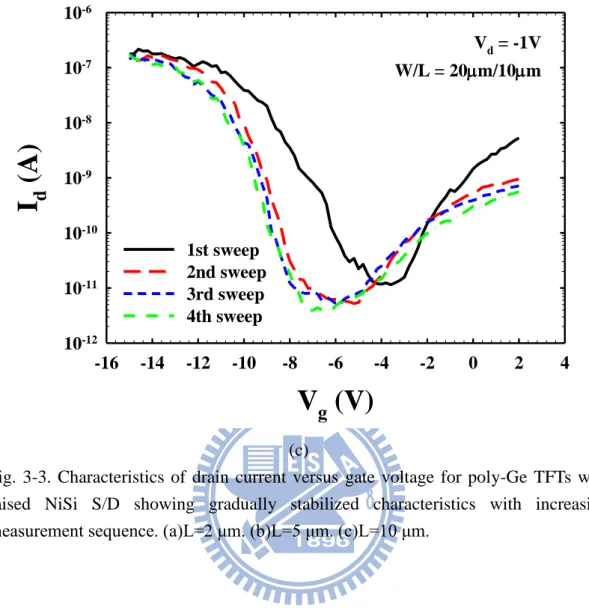
3-1-1 Transfer Characteristics
Figures 3-2 and 3-3 show the transfer curves (Id–Vg) of poly-Ge TFT devices of
different channel lengths (L) with raised S/D materials of poly-Si and NiSi,
respectively. Typically, after several repeated measurements, it can be seen that the
characteristics become stable. Overall, the stabilized transfer curves shift leftwards
with off-state current decreased by 1 ~ 2 orders of magnitude and the subthreshold
swing (S.S.) decreased as compared with the fresh curve. This indicates that there
18
interface in the device. During the first few measurements, some of the carriers will
be trapped by the defects. In addition, charging of these defects results in a transient
current that makes profound contribution to leakage current. In this study, all process
steps were done at low temperature (less than 500℃), including the gate oxide
deposition which was performed by PECVD instead of LPCVD. It is expected that the
quality of oxide/channel interface and the gate oxide are not as good as those in bulk
CMOS devices. Moreover, because the grain size is really small (<5 nm) as shown in
Fig. 3-4 [30], a lot of defects may exist in or near the grain boundaries and the
interface between channel and gate oxide [31], [32].
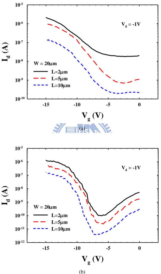
Figures 3-5 (a) and (b) show the stabilized transfer characteristics of the devices
with poly-Si and NiSi S/D, respectively, and channel lengths of 2 μm, 5 μm and 10 μm. The threshold voltage (Vth), calculated by the constant current method, is defined
as the gate voltage needed to achieve a drain current (Id) of (W/L) × 10 nA. The
devices have a threshold voltage of around 8 V, and an Ion/Ioff maximum ratio of 104 to
~105.
In general, the device with shorter channel length usually has a larger off-state
leakage current, which may be caused by the inferior S.S.. However, we don‟t observe
the trend in our case, as shown in Fig. 3-6, in which we can see the S.S. values of the
19
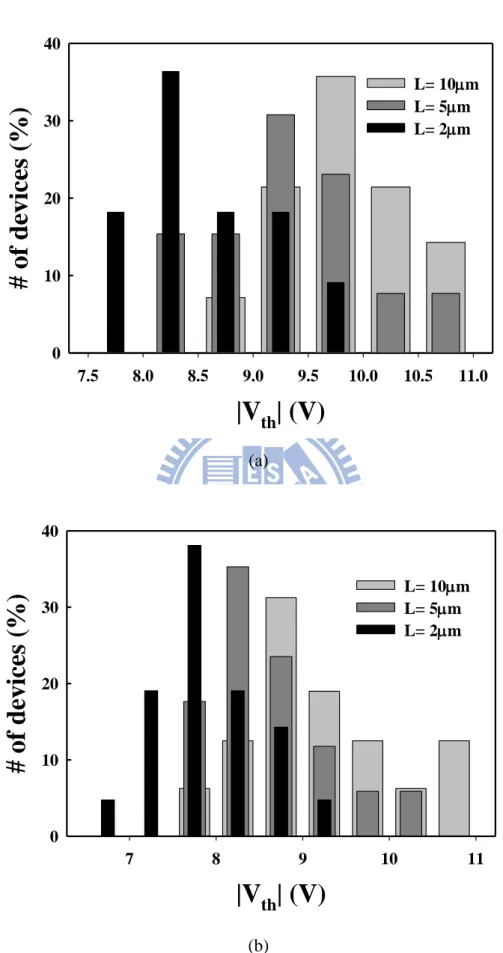
(a) and (b) show the threshold voltage distribution of a poly-Ge TFT device with
poly-Si and NiSi S/D, respectively. Here, the threshold voltage range is widely
distributed from 7.75 V to 10.75 V. The small grain size results in the large Vth and
S.S..
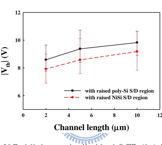
As shown in Fig. 3-8, the mean threshold voltage in poly-Ge TFTs with raised
NiSi S/D is lower than that with raised poly-Si S/D. Both devices are implanted with
BF2+ (see Chapter 2 for detail) at the raised S/D regions to form p+ regions prior to
poly-Ge deposition [33]. The major difference between the two devices is the S/D
materials, namely, poly-Si and NiGe. The smaller Vth in the devices with NiSi S/D
implies the channel crystallinity of the devices is superior to that with poly-Si S/D.
During the SPC treatment, the poly-Si and NiSi are expected to serve as seeding layer
for crystallization. The above results indicate the use of NiSi is better in promoting in
the channel crystallinity.
Figures 3-9 (a) and (b) show the mobility of the two types of TFTs. Based on the
transfer characteristics measured at Vsd = 1 V, the field-effect mobility (μFE) is
determined by Eq. 2-1. Both devices reveal similar and low mobility value. It is noted
that the intrinsic property of poly-Ge is not affected by the S/D structure. Generally,
the hole mobility in bulk Ge reaches 1900 cm2/V-s [34]. And the effective hole
20
respectively [34]-[36]. So the inferior mobility of less than 1 cm2/V-s also reflects the
poor crystalline quality of the Ge layer and interface between the oxide and the
channel. The high series resistance in the S/D is another factor that will lead to the
underestimation of the mobility, which will be discussed in Section 3-2. The
characteristics of poly-Ge TFTs with different raised S/D are summarized and listed in
Table 3-1, including Ion/Ioff ratio, threshold voltage, S.S., and mobility.
3-1-2 Output Characteristics
Effects of the large parasitic resistance in the raised S/D poly-Ge TFTs are more
significant on the output performance. Besides the resistance in the poly-Ge channel
caused by granular structure and defects at the interface between gate oxide and
channel, there are many components of parasitic resistance at the S/D side [37], [38].
The structure in the vicinity of channel end of raised S/D of the device is depicted in
Fig. 3-10 (a). Fig. 3-10 (a) also illustrates the paths at S/D side where the current
passes by. When applying negative biases to the drain and the gate, the current flows
from source to channel and channel to drain.
There are many different resistance components which tend to decrease the on
current, as shown in Fig. 3-10 (b). Impacts of these resistances are reflected on the
21
components. Firstly, Rco is the component of contact resistance. In our devices, there
are at least two such resistance components, one exists at the interface between the
channel and raised S/D region, and the other is in the S/D between Ge and raised S/D
material. It is dependent on the step coverage of the deposited Ge thin film during
fabrication process. Secondly, Rac is the component of accumulation resistance caused
by the doping gradient. Finally, Rsh is the sheet resistance in the S/D, which is
attributed to the poly-Ge crystallinity and raised S/D material quality. Fig. 3-11 also
shows that current is pinched at low-drain bias with the high series resistance.
3-2 Series Resistance and Effective Channel Length
The overall resistance between source and drain consists of the following
components: source resistance, drain resistance, and channel resistance. The source
resistance RS and drain resistance RD are shown in Fig. 3-12 (a). RS and RD are
composed of the source and drain contact resistance, the sheet resistance of the source
and drain, the spreading resistance at the transition from the source diffusion to the
channel and any additional resistance.
Methods proposed in [39]-[42] are taken to extract the RSD and Leff. I-V
characteristics of the device operating in the linear region can be expressed as the
22
1 ' ' ' ' 2 eff D ox GS T DS DS eff W I C V V V V L , (Eq. 3-1)where ID is the drain current, μ is the carrier mobility, Cox is the gate oxide
capacitance, Weff is the effective channel width, Leff is the effective channel length,
V’DS, V’GS and V’T are the intrinsic drain bias, gate bias and threshold voltage,
respectively.
When operating the devices in the linear region, e.g., VD = -1V (relatively low
compared with VT ), with (VGS-VT) >> 0.5VDS and RS = RD = RSD/2. Eq. 3-1 becomes
( ) ( ) ( ) eff eff ox GS T DS D eff eff ox GS T SD W C V V V I L L W C V V R . (Eq. 3-2)
The device resistance (Rm), including intrinsic channel resistance (Rch) and RSD,
can be defined by the following equation,
DS
m ch SD
D V
R R R I . (Eq. 3-3)
According to Fig. 3-12 (b), we can derive an analytical form of the Rm by Eqs. 3-1,
3-2, and 3-3, which is convenient for us to extract Leff and RSD [42].
m eff SD R AL R B A L, (Eq. 3-4) with
1 0.5 ox eff GS T DS C W V V V A , (Eq. 3-5) and SDB R
A
L
, (Eq. 3-6)23
where Δ L = L-Leff .
In this method, a set of devices with same channel width and different gate
lengths are required. Here, we would like to extract the RSD values of devices with
different raised S/D material. With Eqs. 3-4 and 3-5, Rm can be plotted as a function
of L, as shown in Figs. 3-13 (a) and 3-14 (a). Then, we use the linear least square
regression method to fit the data, draw the plot of B versus A, with Eq. 3-6. According
to the regression result, we can obtain the RSD, as shown in Fig. 3-13 (b) and 3-14 (b).
As shown in Figs. 3-13 (b) and 3-14 (b), the extracted RSD of raised poly-Si and
NiSi S/D regions are 0.575 MΩ and 0.490 MΩ, respectively. The ΔL of raised
poly-Si and NiSi S/D region are 1.45 μm 1.90 μm, respectively. A large series
resistance is consistent with our observation in previous chapter. Therefore, the large
S/D resistance restrains the device performance.
Hence, after taking into account the RSD effect of our device, with Eq. 3-2 and
Fig 3-12 (b), VDS should be replaced by V’DS (VDS = V’DS + ID‧RSD). The mobility
becomes 1.96 times and 2.33 times larger than previous calculations. The corrected
mobility values are also shown in Table 3-2.
Furthermore, one thing should be noted in Figs. 3-13 (a) and 3-14 (a) is that the
data points are actually not lying on the fitting straight lines. To explain this, we
24
shown in Fig. 3-15, we consider the raised S/D regions as a seeding layer for
crystallization and enhancing the crystallinity of the Ge-channel. So, the channel can
be roughly divided into two regions, one is neighboring to the S/D seeding region called “Section 1” with length of L1, the other is located at the channel center called
“Section 2” with the length of L2. In Section 2, crystallization of the poly-Ge is
independent of the S/D seeding layer and thus has a poorer crystallinity and therefore
higher resistance.
During the fabrication, the L1 maximum length should be a constant due to same
crystallization process conditions. In Figs. 3-13 (a) and 3-14 (a) for the devices with
shorter channel (e.g, ≦5 μm), Section 1 region would dominate the channel and thus the total resistance is relatively low. When the channel length increases to 10 μm, Section 2 becomes dominant and results in an anomalously high measured resistance.
3-3 Drain Induced Grain Barrier Lowering Effect
In polycrystalline semiconductor films, some electrical conduction models
considering the carrier transport across the grain boundaries (GBs) and the effects of
grain sizes have been developed. In the literatures, Lin et al. [43] had developed a
model to calculate the barrier height at grain boundary. This model takes into account
25
grain barrier lowering (DIGBL). Moreover, this model illustrates that the drain bias
will generate asymmetric grain barrier height and result in more carrier injection from
the lowered barrier side. Besides, Lin et al. also clarified the dependence of threshold
voltage on the grain size, that is, the smaller the grain is, the larger the threshold
voltage will be.
Figs. 3-16 and 3-17 show the ID-VG characteristics under different VDS. As we
can see, when the applied |VDS| increases, the drain current increases and shifts
upward. Though likely, we are not sure that this phenomenon is caused by the DIGBL
effect. To verify our postulation, we take the methods proposed in [44]-[45] to extract the potential barrier, B , at grain boundaries. For a device operated in the
subthreshold region, when applying a lateral voltage VDS to the polycrystalline film,
the voltage drop across a grain-boundary is ΔV = VDS /Ng, where Ng is the number of
grain boundaries in the polycrystalline film across the channel, as shown in Figs. 3-18
[44] and 3-19 [45].
Note that B is modulated by the gate bias and is thus a function of the
surface potential,
V
i. When we consider the thermionic emission process over theenergy barrier, the current density can be expressed with the following equation [44],
g n i B inv i L V V qn J exp( ( )) , (Eq. 3-7)
26
the electron mobility in the surface channel, and
n
inv is the inversion carrierconcentration (
C
OX(
V
GS
V
TO
V
i)
/
qy
inv, whereV
TO is the threshold voltage forbulk material). We also can obtain that
B(
V
i)
is equal to (
b0
V
1), where,2 1 V
V V
as shown in Fig. 3-19, and
b0 is the potential barrier without theapplied drain bias. Furthermore, the voltage drop at the lower barrier side can be
expressed with the following equation [3],
0 1 8 1 2 b V V V . (Eq. 3-8)
Substituting Eq. 3-8 into Eq. 3-7 gives
g n b b inv i L V V V qn J 0 0 8 1 2 exp . (Eq. 3-9)
Then, we set the V VD1 under |VDS| = 1 V, V VD2 2VD1 under
|VDS| = 2 V, and
V
V
D3
0
.
5
V
D1 under |VDS| = 0.5 V. Combining theseconditions, Eq. 3-9 can be rewritten in terms of
V
D1. After calculation, we can express the relation between the ratios of current density under various VDS with thefollowing form: ) 5 . 0 | (| ) 1 | (| ) 1 | (| ) 2 | (| V V J V V J B V V J V V J DS DS DS DS , (Eq. 3-10) with 1 1 0 9 exp 4 64 D D B V V B A
, (Eq. 3-11) and27 2 ) 1 ( ) 5 . 0 ( ) 2 ( ) ( ) )( ( V V i TO GS V V i TO GS V V i TO GS DS DS DS V V V V V V V V V A . (Eq. 3-12)
When VDS is not large, parameter A is less than but very close to 1. Parameter B
can be figured out by substituting the experimental data into Eq. 3-10. Range of the
extracted B values is from 0.7 to 1.4, and most of them are also close to 1. Though
more efforts are still needed to uncover the nature of conduction barriers at the grain
boundaries, the DIGBL effect is still likely the main cause for the significant shift in
ID as the VDS is varied, even as the channel length is long.
3-4 Comparisons among Different Poly-Ge TFT Devices
Through literature survey, there are several groups dedicated to the research of
poly-Ge TFT. Here, we choose some of them published in recent years as references
for comparison with the results obtained in this study. First, Sadoh et al. have
fabricated poly-Ge TFT with NiGe Schottky S/D on glass by low-temperature (<
500℃) processing [46], [47]. Another study was proposed by W. Hsu et al., where
single-crystalline Ge p-channel TFTs with Schottky S/D on flexible polyimide
substrates were fabricated by a simple low-temperature process (≦ 250 ℃) [48].
Based on their respective results, relatively high hole mobility (about 100 cm2/V‧s
[46] and 170 cm2/V‧s [48]) was reported. In this section, we will benchmark the
28
The process flow and schematic cross sections of NiGe Schottky S/D TFTs are
shown in Fig. 3-20 (a) [46], [47]. The Ion/Ioff is ~102 by applying an SOI (silicon on
insulator) structure with an Ion of ~10 μA/μm at Vd = -5V, as shown in Fig. 3-20 (b).
The superior on characteristics of the devices is owing to the much better film
crystalinity with grain size of about 80 nm, which is larger than 5 nm in ours.
Moreover, Ioff is much worse, rendering a poor on/off current ratio. , Such high
leakage is presumably related to the ambipolar conduction of the Schottky NiGe S/D
structures.
In Fig. 3-21 (a), it shows the process flow of forming single-crystalline Ge
p-channel TFTs with Schottky-barrier S/D on flexible polyimide substrates [48]. In
this study, the device has a very small Ion/Ioff ratio of ~22, and an Ion of ~1.6 μA/μm at
Vd = -1.5 V, as shown in Fig. 3-21 (b). The large Ioff is suspected to be related to the
underlying indium tinoxide (ITO) layer which would provide additional leakage
current path. It should be noted that the NiGe S/D is not raised.
According to the work of our group carried out last year [30], whose process
flow and schematic cross sections are shown in Fig. 3-22, the device has an Ion/Ioff
ratio of ~102. The relatively low Ion as compared to the poly-Ge raised S/D TFT
device is mainly ascribed to a large parasitic S/D resistance, as shown in Fig. 3-1. The
29
Moreover, the poly-Si layer under the Ge thin film may also contribute parasitic
current route between the S/D and is also responsible for the large Ioff.
The comparison of characteristics of these poly-Ge TFTs are summarized and
listed in Table 3-3, including Ion/Ioff ratio, threshold voltage, S.S., and mobility. As we
can see, the mobility of our device is inferior to other structures. More efforts in
promoting the film crystallinity are needed. However, the high Ion/Ioff ratio is greatly
30 Table 3-1
Major characteristics of poly-Ge TFT devices.
Ge TFT with raised poly-Si S/D Ge TFT with raised NiSi S/D
L=2μm L=5μm L=10μm L=2μm L=5μm L=10μm Ion/Ioff Ratio ~104 ~105 S.S. (mV/dec) 1954 1809 2272 718 685 829 Vth (V) 8.59 9.37 9.82 7.92 8.57 9.18 μ (cm2 /V-s) 0.66 0.64 0.73 0.57 0.73 0.38 Table 3-2
Corrected mobility by taking into account RSD effect.
Ge TFT with raised poly-Si S/D Ge TFT with raised NiSi S/D
L=2μm L=5μm L=10μm L=2μm L=5μm L=10μm
μ (cm2
/V-s) 0.66 0.64 0.73 0.57 0.73 0.38
μ fix (cm2/V-s) 1.75 1.04 0.8 1.33 0.91 0.41
μ fix: mobility corrected with the series S/D resistance taken into account.
Table 3-3
Major characteristics of different poly-Ge-channel TFT devices.
Ion/Ioff Ratio Vth (V) S.S. (mV/dec) μ (cm2/V-s) Ge TFT with raised S/D 104 ~ 105 ~ -8.5 ~ 800 ~ 1 NiGe Schottky S/D TFTs [46],[47] 10 2 ~ -10 ~ 4000 ~ 100 Ge p-channel TFT on polyimide substrate [48] 22 ~ -3 ~ 1200 ~ 120 poly-Ge on poly-Si film
p-channel TFT [30] 10
2
31
Chapter 4
Conclusion and Future Work
4-1 Summary and Conclusion
In this thesis, we have fabricated and characterize poly-Ge TFT devices with
raised NiSi or poly-Si S/D. The poly-Ge channel was formed with SPC method at a
lower temperature (<500 ℃ ). Due to the existence of defects at or near the
channel/oxide interface, the device characteristics are not stable until several repeated
measurements are executed. The transfer curve is stabilized because during the first
few measurements the traps are filled by the carriers and become inactive. The
stabilized transfer curves shift leftwards with off-state current decreased by 1 ~ 2
orders of magnitude and the S.S. decreased as compared with the fresh curve.
After stabilization, superior device performance with smaller S.S. and Ion/Ioff
ratio of about 105 is achieved. However, due to the small grain size (5 nm), the
threshold voltage range is wide and varies from 7.75 V to 10.75 V. The mean
threshold voltage in poly-Ge TFTs with raised NiSi S/D is lower than that with raised
poly-Si S/D. During the SPC treatment, the poly-Si and NiSi are expected to serve as
32
better in promoting the channel crystallinity.
Besides, there are many different resistance components which tend to decrease
the on-current and are reflected on the output characteristics. The RSD extracted for
raised poly-Si and NiSi S/D are 0.575 MΩ and 0.490 MΩ, respectively. The ΔL
extracted for raised poly-Si and NiSi S/D region are 1.45 μm and 1.90 μm,
respectively. Furthermore, in our devices, it is shown that the crystallinity in the
channel is non-uniform and location dependent, owing to the action of the seeding
layer in crystallizing the α-Ge.
Finally, we have also investigated the ID-VG characteristics under different VDS.
We found that the DIGBL effect is likely the main cause for the significant shift in ID
as VDS is varied, even when the channel length is long.
4-2 Future Work
Using poly-Ge film as the channel material of TFT devices has been
implemented and the characteristics also have been demonstrated. To further enhance
the device performance, some suggestions for future work are listed below.
1. Because of the fine grain size formed by SPC method, the merits of the Ge film
are hard to stand out. In the future we suggest to replace SPC by MIC, MILC or
33
could even be reduced.
2. The conditions of forming raised S/D region in our study have not been optimized
yet. More efforts are needed to understand the impacts and influences of the S/D
materials on device characteristics in terms of junction properties, parasitic
34
References
1. Y. Kamata, “High-k/Ge MOSFETs for future nanoelectronics,” Materials Today,
vol. 11, no. 1-2, pp. 30-38, 2008.
2. E. Gerritsen, N. Emonet, C.Caillat, N. Jourdan, M. Piazza, D.Fraboulet, B. Boeck, A. Berthelot, S. Smith, and P.Mazoyer, “Evolution of materials technology for stacked-capacitors in 65nm embedded-DRAM,” Solid State Electron., vol. 49, pp.
1767-1775, 2005
3. K. Saraswat, C. O. Chui, T. Krushnamohan, D. Kim, A. Nayfeh, and A. Pethe, “High performance germanium MOSFETs,” Mater. Sci. Eng. B, vol. 135, no. 3, pp. 242-249, 2006.
4. C. O. Chui, H. Kim, D. Chi, P. C. McIntyre, and K. C. Saraswat, “Nanoscale
germanium MOS dielectrics – Part II: high-κ gate dielectrics,” IEEE Trans.
Electron Devices, vol. 53, no 7, pp. 1509-1516, 2006.
5. J. H.Park, M. Tada, P. Kapur, H. Peng, and K. C. Saraswat, “A very low
temperature single crystal germanium growth process on insulating substrate
using Ni-induced lateral crystallization for three-dimensional integrated circuits,”
Appl. Phys Lett., vol. 91, 143107, 2007.
6. J. H.Park, M. Tada, P. Kapur, and K. C. Saraswat, “Low temperature boron and
35
crystallization and its application for three-dimensional integrated circuit,” Appl.
Phys. Lett., vol. 93, 183512, 2008.
7. C. O. Chui, K. Gopalakrishnan, P. B. Griffin, J, D. Plummer, and K. C. Saraswat, “Activation and diffusion studies of ion-implanted p and n dopants in germanium,” Appl. Phys. Lett., vol. 83, no. 16, pp. 3275-3277, 2003.
8. D. Kuzum, A. J. Pethe, T. Krishnamohan, and K. C. Saraswat, “Ge (100) and (111)
n- and p-FETs with high mobility and low-T mobility characterization,” IEEE
Trans. Electron Devices, vol. 56, no 4, pp. 648-655, 2009.
9. J. P. Xu, X. F. Zhang, C. X. Li, P. T. Lai, and C. L. Chan, “Improved electrical
properties of Ge p-MOSFET with HfO2 gate dielectric by using TaOxNy
interlayer,” IEEE Electron Devices Lett., vol. 29, no 10, pp. 1155-1158, 2008.
10. E. P. Gusev, H. Shang, M. Copel, M. Gribelyuk, C. D‟Emic, P. Kozlowski, and T. Zabel, “Microstructure and thermal stability of HfO2 gate dielectric deposited on
Ge (100),” Appl. Phys. Lett., vol. 85, no. 12, 2004.
11. S. Iwauchi and T. Tanaka, “Interface properties of Al2O3–Ge structure and
characteristics of Al2O3–Ge MOS transistors,” Jpn. J. Appl. Phys., vol. 10, no. 2,
pp. 260-265, 1971.
12. S. Zhu, R. Li, S. J. Lee, M. F. Li, A. Du, J. Singh, C. Zhu, A. Chin, and D. L.
36
high-gate Dielectric and metal gate,” IEEE Electron Devices Lett., vol. 26, no 2,
pp. 81-83, 2005.
13. Y. Y. Zhang, C. J. Choi, J. Oh, I. S. Han, S. G. Li, K. Y. Park, H. S. Shin, G. W.
Lee, J. S. Wang, P. Majhi, R. Jammy, and H. D. Lee, “Microstructural innovation
of Ni germanide on Ge-on-Si substrate by using palladium incorporation,”
Electrochem. Solid-State Lett., vol. 12, pp. 402-404, 2009.
14. Y. Y. Zhang, J. Oh, I. S. Han, Z. Zhong, S. G. Li, S. Y. Jung, K. Y. Park, H. S.
Shin, W. H. Choi, H. M. Kwon, Wei. Yip. Loh, P. Majhi, R. Jammy, and H. D.
Lee, “Thermal immune Ni germanide for high performance Ge MOSFETs on
Ge-on-Si substrate utilizing Ni0.95Pd0.05 alloy,” IEEE Trans. Electron Devices, vol.
56, no. 2, pp. 348-353, 2009.
15. R. Li, H. B. Yao, S. J. Lee, D. Z. Chi, M. B. Yu, G. Q. Lo, and D. L. Kwong, “Metal-germanide Schottky source/drain transistor on germanium substrate for future CMOS technology,” Thin Solid Film, vol. 504, pp. 28-31, 2006.
16. K. Ikeda, Y. Yamashita, N. Sugiyama, N. Taoka, and S. I. Takagi, “Modulation of
NiGe/Ge Schottky barrier height by sulfur segregation during Ni germanidation,”
Appl. Phys. Lett., vol. 88, 152115, 2006.
17. T. Maeda, K. Ikeda, S. Nakaharai, T. Tezuka, N. Sugiyama, Y. Moriyama, and S.
37
Schottky source/drain,” IEEE Electron Device Lett., vol. 26, no. 2, pp. 102-104,
2005.
18. S. Kobayashi, M. Sakuraba, T. Matsuura, J. Murota, and N. Nikoshiba, “Initial
growth characteristics of germanium on silicon in LPCVD using germane gas,” J.
Cryst. Growth, vol. 174, pp. 686-690, 1997.
19. M. J. Yang, J. Shieh, S. L. Hsu, I. J. Huang, C. C. Leu, S. W. Shen, T. Y. Huang, P.
Lehnen, and C. H. Chien, ” Low-temperature growth of polycrystalline Ge films on SiO2 substrate by HDPCVD,” Electrochem. Solid-State Lett., vol. 8, pp.
C74-C76, 2005.
20. K. Saraswat, C. O. Chui, T. Krishnamohan, D. Kim, A. Nayfeh, and A. Pethe, “High performance germanium MOSFETs,” Mat. Sci. Eng. B, vol. 135, pp. 242-249, 2006.
21. S. Yamaguchi, N. Sugii, and S. K. Park, “Solid-phase crystallization of Si1-xGex
alloy layers,” J. Appl. Phys., vol. 89, no. 4, pp. 2091-2095, 2001.
22. Y. Liu, M. D. Deal, and J. D. Plummer, “High-quality single-crystal Ge on
insulator by liquid-phase epitaxy on Si substrates,” Appl. Phys. Lett., vol. 84, no.
14, pp. 2563-2565, 2004.
23. J. H. Park, M. Tada, P. Kapur, H. Peng, and K. C. Saraswat, “Metal-induced
38
monolithic three-dimensional integration,” J. Appl. Phys., vol. 106, 074510, 2009.
24. A. R. Joshi and K. C. Saraswat, ”Nickel induced crystallization of α-Si gate
electrode at 500°C and MOS capacitor reliability,” IEEE Trans. Electron Device,
vol. 50, no. 4, 2003.
25. J. H. Park, M. Tada, P. Kapur, H. Peng, and K. C. Saraswat, “Self-nucleation free
and dimension dependent metal-induced lateral crystallization of amorphous
germanium for single crystalline germanium growth on insulating substrate,” J.
Appl. Phys., vol. 104, 064501, 2008
26. J. Olivares, A. Rodríguez, J. Sangrador, T. Rodríguez, C. Ballesteros, and A. Kling, “Solid-phase crystallization of amorphous SiGe films deposited by LPCVD on SiO2 and glass,” Thin Solid Films, vol. 337, no. 1-2, pp. 51-54, 1999.
27. K. Toko, I. Nakao, T. Sadoh, T. Noguchib, and M. Miyao, “Electrical properties of
poly-Ge on glass substrate grown by two-step solid-phase crystallization,” Solid
State Electron., vol. 53, pp. 1159-1164, 2009.
28. T. Hiramoto and M. Takamiya, “Low power and low voltage MOSFETs with
variable threshold voltage controlled by back-bias”, IEICE Trans. Electron., vol.
E83-C, pp. 161-169, 2000.
29. Y. Taur and T. H. Ning, “Fundamentals of modern VLSI devices.” Cambridge,
39
30. Y. N. Chang, “Fabrication and characterization of poly-Ge based devices,” Master,
Thesis, Department of Electronics Engineering & Institute of Electronics, NCTU,
2009.
31. M. Kimura, S. Inoue, T. Shimoda, and T. Sameshima, "Current paths over grain
boundaries in polycrystalline silicon films," J. Appl. Phys., vol. 40, pp. 97–99,
2001.
32. T. Kamiya, Y. T. Tan, Y. Furuta, H. Mizuta, Z. A.K. Durrani, and H. Ahmed,
"Carrier transport in ultra-thin nano/polycrystalline silicon films and nanowires,"
Mat. Res. Soc. Symp. Proc., vol. 664, pp. A16.2.1-A16.2.6, 2001.
33. Y. L. Chao and C. S. Woo, “Germanium n+/p diodes: A dilemma between shallow junction formation and reverse leakage current control,” IEEE Trans. Electron Devices, vol. 57, no. 3, pp. 665–670, 2010.
34. K. C. Saraswat, C. O. Chui, T. Krishnamohan, A. K. Okyay, H. Kim, and P. McIntyre, “Ge and SiGe for high performance MOSFETs and integrated optical interconnects,” SSDM, 2004.
35. R. Xie, T. H. Phung, W. He, Z. Sun, M. Yu, Z. Cheng, and C. Zhu, “High mobility
High-k/Ge pMOSFETs with 1 nm EOT - new concept on interface engineering and interface characterization,” IEDM Tech. Dig., pp. 393–396, 2008.
40
E. Van Moorhem, G. Raskin, F. Letertre, T. Billon, M. Meuris, and M. Heyns, ”Optimisation of a thin epitaxial Si layer as Ge passivation Layer to demonstrate deep sub-micron n- and p-FETs on Ge-On-Insulator substrates,”
Microelectron Eng., vol. 80, pp. 26-29, 2005.
37. S. M. Sze and Kwok K. Ng, Physics of Semiconductor Devices, 3rd ed., New York:
Wiley, 2007.
38. Kwok. K. Ng and W. T. Lynch, “Analysis of the gate-voltage-dependent series resistance of MOSFET‟s,” IEEE Trans. Electron Devices, vol. 33, no. 7, pp. 965–972, 1986.
39. K. Terada and H. Muta, “A new method to determine effective MOSFET channel
length,” Jpn. J. Appl. Phys., vol. 18, no. 5, pp. 953-959, 1979.
40. J. G. J. Chern, P. Chang, R. F. Motta and N. Godinho, “A new method to determine MOSFET channel length,” IEEE Electron Device Lett., vol. 1, no. 9, pp. 170-173, 1980.
41. S. E. Laux, “Accuracy of an effective channel length/external resistance extraction algorithm for MOSFET„s,” IEEE Trans. Electron Devices, vol. 31, no. 9, pp. 1245-1251, 1984.
42. D. K. Schroder, Semiconductor material and device characterization, 3rd ed. New
41
43. P. S. Lin, J. Y. Guo, and C. Y. Wu, “A quasi-two-dimensional analytical model
for the turn-on characteristics of polysilicon thin-film transistors,” IEEE Trans.
Electron Devices, vol. 37, no. 3, pp. 666–674, 1990.
44. G. Y. Yang, S. H. Hur, and C. H. Han, “A physical-based analytical turn-on
model of polysilicon thin-film transistors for circuit simulation,” IEEE Trans.
Electron Devices, vol. 46, no. 1, pp. 165–172, 1999.
45. W. J. Wu and R. H. Yao, “A simple model of DIGBL effect for polysilicon films
and polysilicon thin-film transistors,” IEEE Electron Devices Lett., vol. 29, no. 10,
pp. 1128–1131, 2008.
46. T. Sadoh, H. Kamizuru, A. Kenjo, and M. Miyao, “Low-temperature formation
(<500°C) of poly-Ge thin-film transistor with NiGe Schottky source/drain,” Appl.
Phys. Lett., vol. 89, no. 12, p. 192114, 2006.
47. T. Sadoh, H. Kamizuru, A. Kenjo, and M. Miyao, “Ge-channel thin-film transistor
with Schottky source/drain fabricated by low-temperature processing,” Jpn. J.
Appl. Phys., vol. 46, no. 3B, pp. L1250-L1253, 2007.
48. W. Hsu, C. Y. Peng, C. M. Lin, Y. Y. Chen, Y. T. Chen, W. S. Ho, and C. W. Liu, “Flexible single-crystalline Ge p-channel thin-film transistors with Schottky-barrier source/drain on polyimide substrates,” IEEE Electron Device
42
(a)
(b) (c)
(d)
Fig. 2-1. (a) Top view layout of a raised S/D TFT device. (b) Cross-section view of a TFT device with raised poly-Si S/D. (c) Cross-section view of a TFT device with raised NiSi S/D. (d) SEM picture of a TFT device with raised NiSi S/D.
![Fig. 3-1. Transfer curves of two different poly-Ge TFT devices [30].](https://thumb-ap.123doks.com/thumbv2/9libinfo/8226410.170752/58.892.162.711.286.732/fig-transfer-curves-different-poly-ge-tft-devices.webp)
![Fig. 3-4. TEM cross-sectional view of poly-Ge film annealed at 500℃ for 1 hour [30]](https://thumb-ap.123doks.com/thumbv2/9libinfo/8226410.170752/63.892.195.696.273.776/fig-tem-cross-sectional-view-poly-film-annealed.webp)