-1-
國
立
交
通
大
學
電子工程學系 電子研究所
博 士 論 文
元件可靠度的改善及類比電路應用時之影響
Reliability investigation for process improvement and on
analog circuit application
研 究 生:林榮俊
指導教授:雷添福 教授
元件可靠度的改善及類比電路應用時之影響
Reliability investigation for process improvement and on
analog circuit application
研 究 生:林榮俊 Student:Jung-Chun Lin
指導教授:雷添福 博士 Advisor:Dr. Tan-Fu Lei
國 立 交 通 大 學
電子工程學系 電子研究所
博 士 論 文
A Dissertation
Submitted to Department of Electronics Engineering and Institute of Electronics
College of Electrical and Computer Engineering National Chiao Tung University
in partial Fulfillment of the Requirements for the Degree of
Doctor of Philosophy in
Electronics Engineering
i 元件可靠度的改善及類比電路應用時之影響 研究生: 林榮俊 指導教授:雷添福 國立交通大學 電子工程學系 電子研究所 博士班 摘要 隨著半導體工業科技的日新月異,製程技術的快速進步,使各種功能能夠同 時置入於一顆晶片之中的可行性就不斷的在提升,也就是希望利用先進半導體製 程來整合數位和類比功能於單一晶片中,此時對於半導體元件的可靠度除了傳統 數位電路的考量,在類比電路使用時的可靠性的研究也隨之而來,. 本篇論文首先提出在深次微米元件的製程之中的回火條件控制上,時間的控 制比溫度的控制更能有效改善元件熱載子的可靠性問題.當半導體深次微米製程 中,源極工程用到铟(Indium)元素時,可以利用較低的溫度但較長時間的回火條件, 使其均勻擴散來達到源極濃度較低, 源極電場較小進而使其有較佳熱載子的可 靠性與元件特性,與此同時,當考慮系統單晶片對元件有不同功能的要求時,利用 製程與元件模擬軟體的幫助及實際製程的驗證結果,適當的利用源極工程,當元 件尺寸越來越小的時候,大角度的植入可以調整元件通道中二維濃度的變化,從 而改變元件的各項特性,使其具有數位電路需要的大的開啟電流以及較小的靜態 電流,並且同時具備類比電路的高輸出電阻和電壓增益,除此之外透過高電壓加 速測試方法,來比較元件在類比電路的操作特性和傳統數位電子元件操作特性的 差異之處,發現在類比電路時元件操作特性更容易有劣化的現象.進一步比較類 比電路中之重要的參數不匹配特性的變化,發現 NMOS 的電流在遭遇高電壓後與 PMOS 相比,不匹配特性會有明顯劣化或變大的結果.這個現象值得提供給類比電路 設計時電路設計者考慮元件劣化對參數不匹配特性的改變,因電路隨使用時間之 增加而元件劣化對參數不匹配特性的改變,使得數位電路仍正常工作時,但類比電 路因不匹配特性的改變而導致整個電路不能正常工作,也就造成單晶片的失效的 現象.
Reliability investigation on process
improvement and for analog circuit application
Student:Jung-Chun Lin Advisor:Dr. Tan Fu Lei
Department of Electronics Engineering
& Institute of Electronics
National Chiao Tung University
Abstract
The dissertation addresses the issues related to reliability improvement of CMOS device and reliability of CMOS device on the analog circuit application especially the mismatch degradation of devices on the analog circuit.
In the beginning, the effect of post-thermal annealing after indium-halo and As-halo implantation on the reliability of sub-0.1um MOSFETs was investigated. We found that the control of annealing time is more efficient than that of annealing temperature with respect to improving the hot carrier-induced device degradation. The best results of device performance were obtained with post-annealing treatment performed at medium temperatures (e.g., 900℃) for a longer time.
iii
of Id,op (defined based on analog application) is found to be the worst case from room temperature to 125℃. This result should be a valuable message for analog circuit designers. As to the reverse temperature effect, the substrate current (Ib) commonly accepted as the statues for monitoring the drain avalanche hot carrier (DAHC) effect should be modified since the drain current (Id) degradation and Ib variations versus temperature have different trends. For the devices having gate oxide thinner than 20 Å, we suggest that the worst condition in considering hot carrier reliability should be placed at elevated temperature.
Finally, hot carrier stress impact on mismatch properties of n and p MOS transistors with different sizes produced using 0.13 μm CMOS technology is presented for the first time. The research reveals that HCI does degrade matching of nMOSFETs’ properties, but, for pMOSFETs, the changes are minor. Due to matching variation after HCI stress, for analog circuits’ parameters, it is found that the after stress lines of n and pMOSFETs exhibit cross points for both σ (∆Vt,op) and σ (∆Ids,op/Ids,op) drawings. It is suggested that the cross points can be used to indicate the minimal size for n and p pairs to have the same degree of mismatch in designing analog circuits. In addition, the interpretations for the differences in n to pMOSFETs and Ids,op to Ids,sat mismatches are provided with experimental verifications.
Acknowledgement
I would like to thank Prof. Lei for his fruitful discussion and illuminative
comment. I would also like to express my appreciation for my colleagues of UMC for their support and suggestions. Finally thanks for my parents’ continuing encouragement and spiritual support.
v
ٛ ٛ ٛ ٛٛ
Contents
Abstract (in Chinese) ………..……… i
Abstract (in English) ……….………..……… ii
Acknowledgement ……….. ……….……… iv
Contents ………..……… v
Table Captions ………..……… vii
Figure Captions ………..……… viii
Chapter 1 Introduction 1.1 Research Background and Motivation ………... 1
1.2 Organization of this thesis ……….. 5
Chapter 2 Efficient improvement of Hot Carrier-Induced Device’s Degradation for Sub-0.1µm CMOS Technology 2.1 Introduction ………..…… 9
2.2 Experiment ………..……….… 11
2.3 Results and discussion ………. 12
2.3.1 Indium-halo vs boron-halo for nMOSFETs ………. 12
2.3.2 Optimum As-halo structure for pMOSFETs ………. 16
2.4 Summary ... 17
Chapter 3 Influence of Pocket Implant on Digital and Analog Performances of Nano-MOSFET 3.1 Introduction ………...……… 28
3.2 Device fabrication ………..……… 30
3.3 Experimental result and discussion ………..……… 30
3.4 Summary ……… 33
Chapter 4 An Investigation on Hot Carrier Effect at Elevated Temperatures for nMOSFETs of 0.13 um Technology 4.1 Introduction ………...……… 44
4.2 Experimental ……… 45
4.2.2 Core devices ……… 47
4.3 Discussion and Conclusions ……….… 48
Chapter 5 An Investigation on Hot Carrier Effect at Elevated Temperatures for pMOSFETs of 0.13 um Technology 5.1 Introduction ……… 61
5.2 Hot Carrier of PMOSFETs and Related Issues ………..…… 62
5.2.1 PMOS Consideration ……….………..…… 62
5.2.2 Mechanisms ………..…… 63
5.3 Experimental Results and Discussion……… 64
5.4 Conclusions ……….……… 66
Chapter 6 Mismatches after Hot-Carrier Injection in Advanced Complementary Metal-Oxide-Semiconductor Technology Particularly for Analog Applications 6.1 Introduction ……… 85
6.2 Experiments ……….…...……… 86
6.3 Results and Discussion ………..……… 87
6.4 Conclusions ……….……… 92
Chapter 7 Conclusion and Future Work 7.1 Conclusion ……….……… 104
vii
Table Captions
Chapter 4
Table I: The measurement conditions (unit: V) ………50
Chapter 5
Table I: The measurement conditions (unit: V) ……….…… 68
Chapter 6
Figure Captions:
Chapter 2
Fig. 1 (a) Threshold voltage roll-off as a function of effective channel length, and (b)
Ion vs Ioff for B-implanted and In-implanted halo nMOSFETs with various PA. ………18
Fig. 2 Transconductance (Gm) as a function of gate voltage (VG) for B-implanted halo
and In-implanted halo nMOSFETs before and after hot-carrier stress. ….…19
Fig. 3 (a) Subthreshold characteristics and (b) gate leakage (IG) as a function of gate
voltage (VG) for nMOSFET with B-implanted and In-implanted halo structures
before and after hot-carrier stress. ………..….20
Fig. 4 Drain current (ID) as a function of gate voltage (VG) for nMOSFETs with various
post annealing conditions before and after hot-carrier stress. ………21
Fig. 5. Hot-carrier-induced saturated drain current (IDSAT) degradation versus stress time
for nMOSFETs with B-implanted and In-implanted halo structures under various post annealing conditions. ………..22
Fig. 6 Substrate current as a function of drain voltage (VD) for B-halo nMOSFETs and
In-halo nMOSFETs with post annealing. ………...23
Fig. 7 Transconductance (Gm) as a function of gate voltage (VG) As-implanted halo
pMOSFETs with various post annealing conditions before and after hot-carrier stress. ………..24
ix
conditions. ……….……26
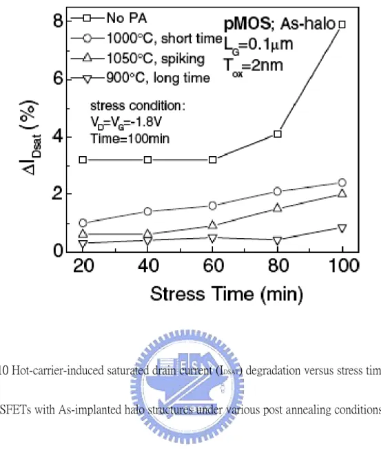
Fig. 10 Hot-carrier-induced saturated drain current (IDSAT) degradation versus stress time for pMOSFETs with As-implanted halo structures under various post annealing conditions. ……….……….27
Chapter 3
Fig. 1: Vt vs. Lg for different pocket implant concentration. ………35Fig. 2: Ion vs. Ioff for different pocket implant concentration. ………36
Fig. 3: Typical drain current and output resistance. ……….…37
Fig. 4: Rout vs. Lg for NMOS IO. ………...38
Fig. 5: Rout vs. Lg for NMOS Core. ………..39
Fig. 6: Gain and Rout vs. Lg for different pocket implant devices. ……….40
Fig. 7: Early voltage and its components versus Vds. ………41
Fig. 8: VA and DIBL vs. Lg for NMOS IO. ………..….42
Fig. 9: VA and DIBL vs. Lg for NMOS Core. ………43
Chapter 4
Fig. 1: Substrate current vs. gate voltage for Vd = 2.2V. ………51Fig. 2: Substrate current vs. gate voltage for Vd = 2.6V. ……….………..52
Fig. 3: Substrate current vs. gate voltage for Vd = 3.0V. ………...…………53
Fig. 4: △Id,sat versus stress time at Vd = 3.0 V with different temperatures. ………..54
Fig. 5: Drain current versus temperature at Vd = 3.0 V after stress 5000 seconds. …55 Fig. 6: △Id,op versus stress time at Vd = 2.2 V with different temperature. …………56
Fig. 7: Drain current degradation versus temperature at Vd = 2.2 V after stress 5000
seconds. ………...57
Fig. 8: Substrate current vs. gate voltage for Vd = 2.2 V. ………..58
Fig. 9: △Id,sat versus stress time at Vd = 2.2 V with different temperatures. ………..59
Fig. 10: Drain current degradation versus temperature at Vd = 2.2 V after stress 5000 seconds. ……….60
Chapter 5
Fig. 1: △Id,lin versus stress time at Vd = -2.0 V at different temperatures. ………...….69Fig. 2: △Id,sat versus stress time at Vd = -2.0 V at different temperatures. ……..70
Fig. 3: △Id,op versus stress time at Vd = -2.0 V at different temperatures. ……….71
Fig. 4: Drain current degradation versus temperature at Vd = -2.0 V after stress 3000 seconds. ………...…72
Fig. 5: △Id,lin versus stress time at Vd = -3.2 V at different temperatures. ………73
Fig. 6: △Id,sat versus stress time at Vd = -3.2 V at different temperatures. ………74
Fig. 7: △Id,op versus stress time at Vd = -3.2V at different temperatures. ……….75
Fig. 8: Drain current versus temperature at Vd = -3.2V after stress 3000 seconds. ……76
Fig. 9: △Id,lin versus stress time at Vd = -3.2 V at different temperatures. ………77
Fig. 10: △Id,sat versus stress time at Vd = -3.2 V at different temperatures. …………..78
xi
Fig. 15: Vt,lin shift of I/O devices (CHC) versus stress time. ………83
Fig. 16: Id degradation of core devices versus stress time. ……….…84
Chapter 6
Fig. 1. Vt,op mismatches vs 1/(W*L)^0.5 gate area. Channel length/width and before or after stress of the tested data are indicated. The cross point of n and p MOS after-stress lines indicate the minimal size at which devices with a 0.15 um channel length will have the same or smaller mismatches. ………..95 Fig. 2. Ids,op mismatches vs 1/(W*L)^0.5 pgate area. The notation is the same as in Fig. 1. Note that the values of nMOSFET pairs particularly on L = 0.15 um devices are much more aggravated than those of pMOSFET pairs after stress although they possess higher degrees of mismatch initially. ………..96 Fig. 3. Time history of mismatches of ∆Vt,op of each transistor pair and means of Vt,op shifts of tested nMOSFETs. The mismatches and particularly the means of Vt,op shifts increase with stress time for nMOSFETs of L = 0.15 um. The data at t = 1 s corresponds to the mismatch before HCI stress. This is also applicable for Figs. 4 to 8. ………..97 Fig. 4. Time history of mismatches of ∆Ids,op/Ids,op of each transistor pair and means of Ids,op degradation ratios of tested nMOSFETs. The mismatches and the means of Ids,op degradation ratios increase with stress time for nMOSFETs of L = 0.15 um. ………...………98 Fig. 5. Time history of mismatches of ∆Vt,op of each transistor pair and means of Vt,op shifts of tested pMOSFETs. The Vt,op mismatches due to HC show different trends for different sizes, and the means of Vt,op shifts abnormally switch back
and forth across the zero line and are smaller compared with those of nMOSFETs. ………99 Fig. 6. Time history of mismatches of ∆Ids,op/Ids,op of each transistor pair and means of Ids,op degradation ratios of tested pMOSFETs. The Ids,op mismatches due to HC show different trends for different sizes, and the means of Ids,op shifts are smaller compared with those of nMOSFETs. ………..100 Fig. 7. Time history of mismatches of ∆Ids,sat/Ids,sat of each transistor pair and means of Ids,sat degradation ratios of tested nMOSFETs. The variations of mismatches and the means of Ids,sat degradation ratios are smaller than those of Ids,op in Fig. 4. ……….101 Fig. 8. Time history of mismatches of ∆Ids,sat/Ids,sat of each transistor pair and means of Ids,sat degradation ratios of tested pMOSFETs. The variations of mismatches and the means of Ids,sat degradation ratios are smaller than those of Ids,op in Fig. 6. ……….102 Fig. 9. Schematic illustration showing that velocity saturation length ∆L will cover
1
Chapter 1
Introduction
1.1 Research Background and Motivation
The integrated circuit (IC) industry has followed a steady path of shrinking device geometries for more than 40 years. It is widely believed that this process will continue for at least another ten years. According to the International Technology Roadmap for Semiconductor (ITRS), by extending this device scaling and increased functionality scenario to the year 2014, minimum feature sizes are projected to be 32 nm and chips with >1011 components are expected to be available. However, there are increasingly difficult materials and technology problems to be solved over the next decade if this is to actually occur and, beyond ten years, there is great uncertainty about the ability to continue scaling metal-oxide-semiconductor field-effect transistor (MOSFET) structures. The industry is also growing from major digital logic circuit to System on a Chip (SoC) era. The major issues need to be handled on the difference operation requirements for devices used between digital and analog circuit in the same time.
In the development of 0.1um technology, the drain engineering is important to match the device universal curve (Ion-Ioff) and Vt roll-off. The major approach will
be used the indium implant to achieve this purpose with less lateral diffusion due to it more heavy ion mass or less diffusivity.
The Indium implant will also cause large silicon interstitial so it will need the post thermal anneal to eliminate the interstitial due to the implant. But the thermal budget is sensitive with respect to anneal time and temperature condition. In this chapter it will be show the combination of anneal temperature and anneal time with the device performance and HCI reliability to find the best condition will be the time to anneal the interstitial.
Secondly, we investigate the degradation of parameter for analog circuit application used. The hot-carrier degradation of N/P MOSFET’s is investigated from the viewpoint of analog operation. Applying sensitive measurement methods was taken to determine (The parameters are investigated to) drain current, drain conductance, and transconductance in the saturation regime besides the commonly investigated parameters in the linear regime of operation.
On the basis of previous research activities, lifetime criteria for hot-carrier-stressed MOSFET’s have undergone changes. They generally aim for a
3
parameters to characterize the damage, and the extrapolation to duty cycles and voltages of operation can be defined in an appropriate way. The important case of analog applications has not yet reached the dame status of knowledge, since analog CMOS applications differ from digital ones in a number of points, as listed below.
1) Operation point: Analog devices usually operate in the saturation region with a quasistatic low gate voltage. Thus neither a relaxation of reliability criteria due to field-assisted detrapping during off-state periods can be considered nor a duty-cycle-factor applied. Moreover, we like to point out that the analog operation region includes the gate voltage range with maximum degradation.
2) Device parameters important for analog operation: Besides the current drive capability, which is the most important device parameter for digital operation, the small signal parameters are of similar or even greater significance in the analog case. Of prime importance are the differential drain output conductance Gds = ∆Id/∆Vd and the transconductance gm = ∆Id/∆Vg, which determine important parameters in analog circuits such as gain, frequency response, linearity and harmonic distortion. Moreover, good matching is an essential demand, since in analog circuits this property is responsible for the accuracy of differential stages and current mirrors. As a consequence the
maximum allowable parameter changes in analog circuits due to hot-carrier degradation are often much smaller than in digital applications, where dot-carrier induced parameter changes of 5 or 10% are frequently used lifetime criteria.
3) Channel length: In order to improve the matching behavior, channel lengths used in analog circuits are usually a few times greater than the minimum channel length allowed by the process technology. For those greater lengths also the small signal parameters are improved.
Then, it was also investigated the mismatch degradation after HCI stress for analog circuit application. It is the first time that the mismatch behaviors are investigated after the HCI stress. From this work, it could provide an important design guideline to reduce the circuit failure coming from mismatch value increased after the product used for a certain time.
Device mismatch is too often treated as part of the black art of analog design. However, extensive studies into the matching behavior of devices have yielded a good understanding of the underlying physical phenomena and offer designers quantitative
5
literature show that matching improves with increasing device area. As a result, accuracy requirements impose a minimal device area and this paper explores the impact of this constraint on the mismatch performance of general analog circuits after stress.
1.2 Organization of This Thesis
This thesis is organized into seven chapters.
Following the introduction, the effect of post-thermal annealing after indium-halo implantation on the reliability of sub-0.1-um nMOSFETs was investigated. We found that the control of annealing time is more efficient than that of annealing temperature with respect to improving the hot carrier-induced device degradation. The best results of device performance were obtained with post-annealing treatment performed at medium temperatures (e.g.,900 C) for a longer time.
Chapter 3 presents analog device design in deep submicron regime is particularly challenging due to conflicting digital performance requirements and the circuit requirements in analog applications. To optimum digital and analog performance for SoC is important. Pocket or halo designs used in high performance digital CMOS design can improve short channel effect (Vt roll-off) but degrade analog device
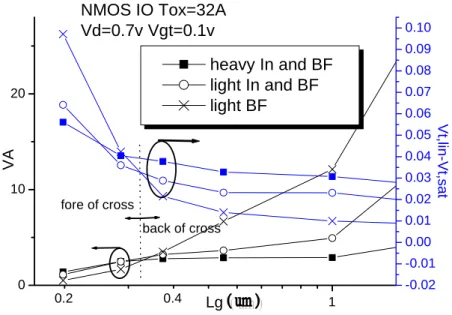
performance. It is shown that the device transconductance (gm), output resistance (Rout) and Early voltage have a crossover phenomenon to gate length variations with different pocket. The Early voltage is divided in two parts, VA of fore cross due to CLM[1] and VA of back cross due to DIBL[2][3][4]. This paper presents non-uniform channel doping have distinct design concept with gate length variations to optimize the Early voltage by diverse pocket implantation experiments.
Chapter 4 describes n-channel metal–oxide–semiconductor field-effect transistors (nMOSFETs) having 20 and 32A˚ gate oxide thicknesses of 0.13 um technology were used to investigate DC hot-carrier reliability at elevated temperatures up to 125 C. The research also focused on the degradation of analog properties after hot-carrier injection. On the basis of the results of experiments, the hot-carrier degradation of Id,op (drain current defined on the basis of analog applications) is found to be the worst case among those of three types of drain current from room temperature to 125 C. This result should provide valuable insight to analog circuit designers. As to the reverse temperature effect, the substrate current (Ib) commonly accepted as the parameter for monitoring the drain-avalanche-hot-carrier (DAHC)
7
should be placed at elevated temperatures.
. Chapter 5 presents DUT under stress conditions were set at temperature 25 ℃, 75 ℃ and 125 ℃, and Vg biased at peak substrate current and maximum gate voltage as drain voltage. It is found that the pMOSFET’s hot carrier mechanism is no longer dominated by negative oxide charges. Comparing different stress modes, the stress with the maximum gate voltage and the higher temperature cause the most severe current degradation. As a result, peak substrate current may not directly indicate hot carrier effect anymore, which is inconsistent with the conventional concept. After comparing all the drain currents, it is found for first time that Id,op is the worst among three kinds of currents. Such message should be valuable for analog circuit designers to have their circuits exhibiting satisfactory reliability.
Chapter 6, hot carrier stress impact on mismatch properties of n and p MOS transistors with different sizes produced using 0.15 µm CMOS technology is presented for the first time. The research reveals that HCI does degrade matching of nMOSFETs’ properties, but, for pMOSFETs, the changes are minor. Due to matching variation after HCI stress, for analog circuits’ parameters, it is found that the after stress lines of n and pMOSFETs exhibit cross points for both σ (∆Vt,op) and σ (∆Ids,op/Ids,op) drawings. It is suggested that the cross points can be used to indicate the minimal size for n and p pairs to have the same degree of mismatch in designing
analog circuits. In addition, the interpretations for the differences in n to pMOSFETs and Ids,op to Ids,sat mismatches are provided with experimental verifications.
9
Chapter 2
Efficient improvement of Hot Carrier-Induced Device’s
Degradation for Sub-0.1
µm CMOS Technology
2.1 Introduction
The reduction in threshold voltage with decreasing channel length is widely used as an indicator of the short-channel effect (SCE) in evaluating complementary-metal oxide-semiconductor (CMOS) technologies.[1] Since metal-oxide-semiconductor field-effect-transistors (MOSFETs) are being scaled down to 0.1 umm and below, this adverse Vth roll-off effect may be a major limitation on deep-submicron-device performance. Thus, finding ways to suppress the SCE while maintaining sufficiently low Vth is a key to working with sub-0.1 um MOSFETs because it is essential to manufacturability and reducing system power needs.[2] In order to control the SCE in the sub-0.1 um regime, it is necessary to reduce gate oxide thicknesses and source/drain extension-junction depths. However, the possibility of direct tunneling limits the extent to which gate oxide thicknesses can be reduced,[3] and reducing source/drain extension junction depths through lowering thermal budgets gives rise to the dopant activation problem, which refers to degradation of device driving
capabilities. In this context, lateral channel engineering gives an extra degree of freedom in efforts to limit adverse SCE effects.[4] Recently, locally high doping concentrations in channels near source/drain junctions have been employed via lateral channel engineering, e.g., halo,[5] pocket,[6] tilted-channel implantation (TCI).[2] and tilted implantation punchthrough stopper (TIPS).[7] These implantations introduce the same types of impurity used in channel regions following gate-etching, which can be symmetrical[6][7] or asymmetrical[8] with respect to the deep source and drain implants. Engineering channel dopant profiles for localized halo implants have been used extensively in deep-submicron CMOS work and has become indispensable for achieving sub-0.1 um CMOSFETs.[9] Indium (In) has been successfully used in fabricating abrupt nMOSFET profiles because of its low diffusion constant,[10] which leads to shallower deep-submicron-nMOSFET source-drain extension/halo profiles. Unfortunately, interstitial Si is introduced during In implantation resulting in an increase in leakage current and degradation of device performance.[11] Besides, the hot-carrier-induced device’s degradation was also enhanced; thus, a post-thermal annealing (PA) treatment after In-halo implantation is
11
B-halo nMOSFETs, In-halo nMOSFETs, and As-halo pMOSFETs. The effect of PA on hot-carrier-induced device’s degradation was also investigated for these CMOSFETs. We propose an appropriate PA for In-halo nMOSFETs and As-halo pMOSFETs to obtain high performance as well as good reliability for sub-0.1 um CMOSFETs.
2.2 Experiment
Devices with channel lengths as small as the sub-0.1um range were fabricated on 8-in wafers (resistivity: 15–25 Ωs/cm) using the conventional CMOSFET twin-well process. After shallow-trench isolation techniques, n/p-wells were formed using MeV-implanted phosphorus (P) and boron (B) ions. Dual-gate CMOSFETs were fabricated using nitrided gate oxide (electrical oxide thickness ~ 25 A), grown by rapid thermal oxidation in NO ambient followed by poly-Si layer deposition. After gate patterning, n/p source/drain extensions were formed using, respectively, arsenic (As) and B-implantations. Then, tilted-angle halo-implantation was applied at 20–30 deg using B (at 10–30 keV, 2-5 x 1013 cm-2) and In (at 120–180 keV, 1-3 x 1013 cm-2) to produce nMOSFETs, and As (at 110–130 keV, 2-4 x 1013 cm-2) to produce pMOSFETs. After halo implantation, various annealing schemes were employed using rapid thermal processing (RTP) at 900 to 1050 C for various !
annealing times. A thin liner oxide was deposited at 500 to 900 C, followed by !
SiN-spacer deposition at 400 to 800 C. After formation of a 0.1 um-thick composite !
liner-oxide/SiN spacer, n+/p+ deep source/drain junctions were formed using As (at 40–60 keV) and B (at 6–10 keV) ion implantation. Finally, the wafers were annealed
!
using RTP at 1000 C followed by CoSi2 salicidation processing, and then completed
using standard backend flow processing. To investigate the hot-carrier effect, device stressing and measurements were carried out on a probe station at various drain voltages (|V| = 1.2-2.0V) and gate voltages (|V| = 0-1.8V) with a stressing time ranging from 0 to 100 min.
2.3 Results and discussion
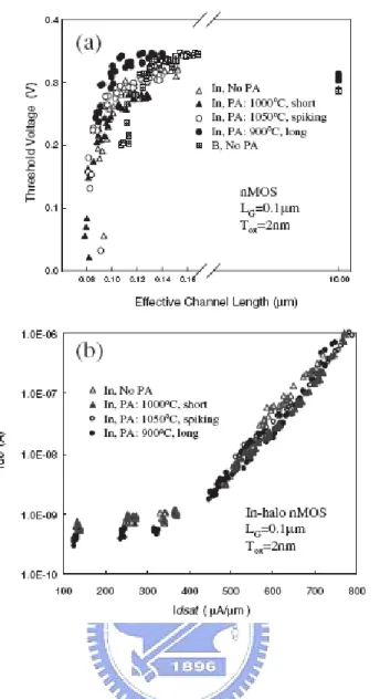
2.3.1 Indium-halo vs boron-halo for nMOSFETs
Threshold voltages, obtained using the Gmmax method, are shown plotted
against effective channel lengths (Leff) in Fig. 1(a). Compared to B-halo-structure
devices, the In-halo samples formed localized high-dose halo structures because of their low diffusion constants, improving the punchthrough margins of the
13
was effectively suppressed in the In-halo samples [12][13] due to indium deactivation. [14] Thus, In-halos allow Vth reductions while increasing device resistance to SCEs. Large amounts of interstitial Si are generated by As-extension implantation and enhanced by In-halo implantation. These Si interstitials can react with the In dopant more efficiently, resulting in a more pronounced deactivation, and causing accelerated Vth roll-offs in short channel devices.[15] Thus, PA is proposed to remove these Si interstitials and suppress the TED phenomenon. Although high-temperature (>1000 ℃) annealing is conventionally used for sub-100 nm device fabrication, junction depths will be
!
increased after 1000 C RTP annealing, resulting in higher device Vth roll-offs. In this study, we found device SCEs can be improved by annealing at 900 ℃ for longer periods of time (>1 min.). It is believed that Si interstitials can be removed by medium-temperature annealing for appropriately longer times without degrading device SCEs. In this work, higher saturation Vths and RSCEs apparently occurred in In-halo nMOSFETs annealed at 900 C for longer periods !
of time. Medium-temperature annealing can improve In-halo device SCEs, even in the sub-0.1 µm-channel-length range, thus reducing the device’s off-state drain current (IDos). Figure 1(b) illustrates that the IDo of devices can be reduced
apparent RSCE occurred in In-halo nMOSFETs at 900 C with longer time !
annealing, improving the In-halo device’s SCE. We believed that the Si interstitial can be removed by medium-temperature annealing for an appropriately longer time without degrading the device’s SCE. Previous work15) had shown that the mobility of In halo nMOSFETs was better than that of the B-halo device particularly at Leff less than 0.1um. Although the localized In-halo
dopant was located only around the extension junction without degrading the device’s driving capacity, the hot-carrier effect of the In-halo device was still a problem and became more serious as the device dimensions decreased. In comparison with B-halo nMOSFETs, the hot carrier-induced Gm degradation of In-halo nMOSFETs becomes more serious after hot-carrier stress particularly at higher gate voltages, as shown in Fig. 2. By the way, the In halo device shows worse subthreshold characteristic and degradation after hot-carrier stressing particularly at higher gate voltages, as shown in Fig. 3(a). After hot-carrier stressing, the device’s subthreshold slope was degraded by 20mV/dec (100 -> 120mV/dec) for In-halo nMOSFETs and 7mV/dec (97 -> 104mV/dec) for B-halo
15
been reported [16] that GIDL is a direct result of the generation of interface states; thus, the largest degradation in IDsat coincides with the largest increase in
interface state density. Thus for In-halo nMOSFETs, worse subthreshold characteristics with larger Ido and GIDL are found. Furthermore, the gate leakage of the In-halo device was also larger than that of the B-halo device, and increased after hot-carrier stress particularly at a higher gate voltage, as shown in Fig. 3(b). It is presumably because a larger interface state was found for the In-halo nMOSFET, thus the In-halo device characteristics and reliability were degraded and then aggravated after hot-carrier stress. In this work, the In-halo device’s subthreshold swing and Ido can be improved with PA particularly at
!
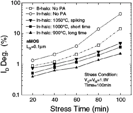
900 C with longer time annealing, as shown in Fig. 4. Figure 5 reveals that the hot-carrier-induced saturated drain current (Idsat) degradation of In-implanted nMOSFETs was more serious than that of B-implanted nMOSFETs. With an appropriate PA, the Idsat degradation of all In-implanted devices can be improved to be lower than that of B-implanted devices. For In-halo nMOSFETs, very low drain degradation (<3%) was obtained by PA at medium temperature with sufficient annealing time. For sub-0.1 um nMOSFETs, the interstitial defect caused by In-halo implantation and the channel impact ionization caused by electrons can be suppressed with PA; thus, In-halo nMOSFETs with PA have a
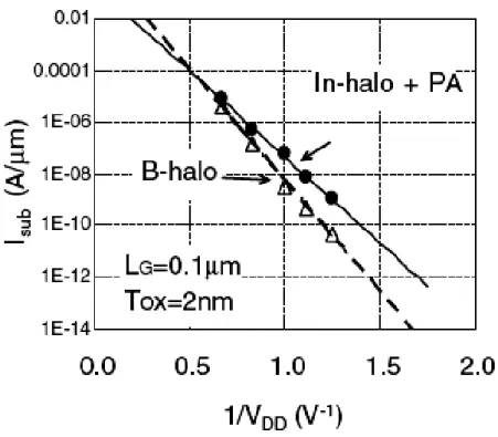
longer lifetime with a lower substrate current (ISUB) than B-halo nMOSFETs
particularly at stress voltages larger than 1.5 V, as shown in Fig. 6.
2.3.2 Optimum As-halo structure for pMOSFETs
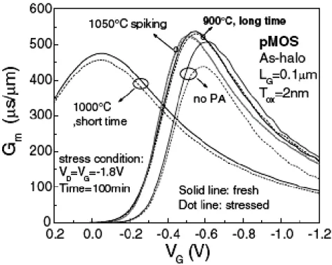
As-halos can be used to fabricate effective pMOSFETs drain structures which can block B-extension efficiently. For pMOSFETs, Si interstitials still occur after As-halo implantation. These Si interstitials degrade device performance and enhance the hot-carrier effect. Thus, an appropriate PA is necessary to alleviate these problems. However, B-extension/As-halo structures are easily degraded by post-thermal treatment owing to the rediffusion channel boron-doping profile, apparently causing the pMOSFET’s threshold voltage (Vt)
!
shift particularly at a PA using 1000 C annealing, as shown in Fig. 7. It is apparent that the hot-carrier-induced Gm degradation can be improved particularly with PA at 900 C with a longer annealing time without degradating !
the device characteristics after hot-carrier stress. Furthermore, the pMOSFET subthreshold characteristics can also be improved with this appropriate annealing,
17
gate leakage can be improved apparently particularly at 900 C with longer time !
annealing; thus, lower interface defects can be removed using this appropriate post-treatment, suppressing the hot-carrier-induced device degradation. Figure 10 shows the hot-carrier-induced Idsat degradation of As-halo pMOSFETs after 100 min stressing with and without post-annealing. It is noted that the hot-carrier-induced Idsat degradation of As-halo pMOSFETs can be improved
!
using an appropriate PA particularly at 900 C with longer annealing time. Thus, very low drain degradation (<1%) can be obtained by PA at medium temperatures with sufficient annealing time.
2.4 Summary
In this brief, the post-thermal annealing effect impact on devices characteristic as well as hot-carrier-induced reliability of 0.1 um CMOSFETs was inspected. The Si interstitial caused by In-halo and As-halo implantation can be removed by PA with enough annealing time. For In-halo nMOSFETs as well as As-halo pMOSFETs, device characteristics and hot-carrier-induced device degradation can be improved by post-annealing particularly at medium temperatures with long time annealing without degrading the device performance.
Fig. 1 (a) Threshold voltage roll-off as a function of effective channel length, and (b) Ion vs Ioff for B-implanted and In-implanted halo nMOSFETs with various PA.
19
Fig. 2 Transconductance (Gm) as a function of gate voltage (VG) for B-implanted halo and In-implanted halo nMOSFETs before and after hot-carrier stress.
Fig. 3 (a) Subthreshold characteristics and (b) gate leakage (IG) as a function of gate voltage (VG) for nMOSFET with B-implanted and In-implanted halo structures before and after hot-carrier stress.
21
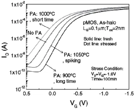
Fig. 4 Drain current (ID) as a function of gate voltage (VG) for nMOSFETs with various post annealing conditions before and after hot-carrier stress.
Fig. 5. Hot-carrier-induced saturated drain current (IDSAT) degradation versus stress time for nMOSFETs with B-implanted and In-implanted halo structures under various post annealing conditions.
23
Fig. 6 Substrate current as a function of drain voltage (VD) for B-halo nMOSFETs and In-halo nMOSFETs with post annealing.
Fig. 7 Transconductance (Gm) as a function of gate voltage (VG) As-implanted halo pMOSFETs with various post annealing conditions before and after hot-carrier stress.
25
Fig. 8 Subthreshold characteristic for As-implanted halo pMOSFETs with various post annealing conditions before and after hot-carrier stress.
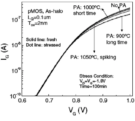
Fig. 9 Gate leakage (IG) as a function of gate voltage (VG) for As-implanted halo pMOSFETs before and after hot-carrier stress under various post annealing conditions.
27
Fig. 10 Hot-carrier-induced saturated drain current (IDSAT) degradation versus stress time for pMOSFETs with As-implanted halo structures under various post annealing conditions.
Chapter 3
Drain Engineering Optimization for Nanometer nMOSFETs
on Mixed Signal Application
3.1 Introduction
The scaling of CMOS technology in nanometer regime has enabled to integrate the RF/analog and digital CMOS function together. Most of the analog applications rely on the pure digital CMOS technology [1]. The scaling of CMOS devices also reveals some difficult challenges, particularly for mixed signal system-on-chip (SoC) applications due to the tradeoff in design requirements for analog and digital applications. The key requirements for analog circuits are the signal swing, linearity, power dissipation, dynamic range (DR), bandwidth (allowed operating frequency), signal-noise-ratio (SNR), linearity, and reliability. Unfortunately, inherent tradeoff among the device parameters like threshold voltage (Vth), short channel effect (SCE), drain-induced barrier lowering (DIBL), transconductance (gm), output resistance (Rout), early voltage (VA), voltage gain
29
high gm, and high gm/Id ratio are required. They can be achieved through strict control of SCE in deep submicron regime. On the other hand, performance of analog circuits critically depends on achieving a high VA. High digital performance like good
current drive-to-off state leakage tradeoff and SCE control are required, but often result in poor analog performance in terms of low output resistance, voltage gain, transconductance-to-drive current ratio, and matching properties [2].
Many solutions were suggested either with multiple threshold voltage designs that employed low doped substrates or with multiple gate-oxide thicknesses to accommodate higher power supplies for analog applications in SoC technology [3], [4]. However, these solutions are not sufficient for the long term due to their obvious impact on SCE and processing difficulties leading to degraded device performance. Thus, the asymmetric channel structures or single pocket (SP) were suggested for mixed signal applications [6]. They have shown good SCE control and Vth roll-off compared to the double pocket or super halo devices as well as super steep retrograde (SSR) devices [5], due to their laterally asymmetric channel doping profile that suppresses SCE and exploiting velocity overshoot to improve current drive. They also have shown better analog performance with increased output resistance and voltage gain over the SSR devices. Although the SP device does not need to compromise the requirements for analog and digital applications, it needs more masks than double
pocket device and result in cost increasing.
In order to optimize analog and digital performance of conventional device structure with double pocket implant devices, different pocket structures have been investigated. How to optimize those analog and digital requirements using ISE TCAD [5] will be presented later.
3.2 Device fabrication
MOSFETs fabricated using high performance 0.13um logic process is used to compare diverse pocket process optimized for high Idrive and good analog performances voltage gain. There are two pocket implant BF2 and In were carried out after the gate stack formation at the same device.
3.3 Experimental result and discussion
The threshold voltage independence on Lg is excellent Vth characteristics. Fig1 and Fig2 show Vth vs. drawn gate length (Lg) and Ion vs. Ioff respectively for diverse pocket implant doping concentration. The heavy pocket doping could lead to high
31
could compress off current while keeping Ion current fixed
In analog circuit applications, the voltage gain is directly proportional to Rout .In [8], it’s shown existing analytical models for MOSFET Rout are not adequate, because only channel length modulation effect is included. Here, we notice, The Rout curve can be clearly divided into four regions with each region dominated by a mechanism in Fig3 be shown .It is worth noting that the second region is the near-saturation region dominated by CLM. The third region is dominated by DIBL and the fourth is the high field region in which Rout is greatly reduced by the substrate current induced body effect (SCBE).[8] In this case, Rout is continual raise so that SCBE could be neglected.
In view of foregoing concept, let us then consider that the variation of Rout with different pocket and LDD process devices to Lg at the same Vgst (Vgs-Vt=0.1 V) and Vd bias which Vd=0.7 V for IO and Vd=0.6v for Core. It is shown in Fig4 and Fig5. It clearly shows that cross phenomenon. The different devices structure and process could move the cross points to gate length. Hence, the Rout at least should be differentiated into two physic effect. We believe that different channel length could lead to change of physic mechanism boundary of Fig3. The fore and back cross due to CLM and DIBL respectively. The concept of Rout to variable Lg should be changed as well. The most important characteristics of Rout in analog circuit designs are the maximum Rout which determines the maximum available gain from the device. Fig6
shows the gain of wide part dependence on the Rout. To obtain the high gain devices have different notions in distinct Lg. The lighter pocket implant concentration could induce high Rout and gain at after of cross. Adversely, that could induce poorer Rout and gain at before of cross.
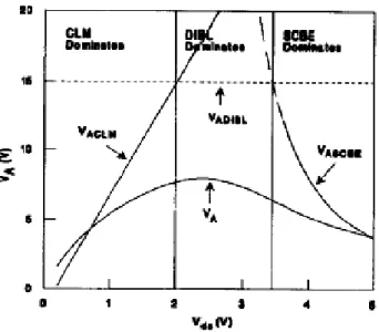
VA has three components, i.e., VACLM, VADIBL and VASCBE, corresponding to CLM, DIBL and SCBE, respectively. Each component can be evaluated separately.[8]
] | ) ( | ) ( | ) [( 1 1 SCBE V I DIBL V I CLM V I I V ds ds ds ds ds ds dsat A ∂ ∂ + ∂ ∂ + ∂ ∂ = ASCBE ADIBL ACLM V V V 1 1 1 + + = (1)
The individual component of VA together with the resultant VA is shown in Fig7. The dominant mechanism is the one with the smallest Early voltage in each region.
In this case of VA which obtaining by intersection of X axis with tangent of Vd bias at 0.7V and 0.6V for IO and Core could exclude VASCBE because of this Vd bias is not enough to induce substrate current. For experimental data in Fig8 and Fig9 these are similar to the Rout that VA appears cross points around 3 time technology node to
33
The concept of VA of fore cross due to CLM dominated. The length ∆L of the pinch-off region increases by an expansion in the direction of the source end with lighter pocket doping concentration and effective channel length has been reduced by ∆L at the same bias condition. In other word, the ∆L increase with decreasing pocket dose concentration could reduce VA. CLM is not a special short-channel phenomenon, but its relative importance becomes distinctly more pronounced at short gate lengths. This is traditional notion for design VA , but the concept of back cross is in conflict with pocket implant concentration. For long channel devices of back cross, despite CLM and DIBL should slowly be negligible. However, large residual DIBL exists at back cross for the pocket devices in Fig8, dominating the VA values which function (1). In these dimension, higher pocket doping concentration lead to Vt,sat shift even more. The conventional explanation of channel length modulation is not entirely valid in pocket devices. Hence, these new observations have a significant impact on design of VA by cross phenomenon of the pocket device. Anyway, the experimental results from pocket device are shown in Fig8 and Fig9. It can be seen that these devices have lower DIBL leading to higher VA at back cross. Adversely, leading to poorer VA at fore cross.
3.4 Summary
concentration for digital CMOS technology and then found out the interesting cross points, which imply pocket implants affect at least have two physic mechanisms CLM and DIBL. The conventional explanation of channel length modulation is not entirely valid in pocket devices. Hence, these new observations have a significant impact on design of VA and Rout. The concept of back cross differs from CLM so that the analog device design for pocket implant must be notice. The lighter pocket implant concentration could induce higher Rout, gain and VA at back of cross. On the other hand, the heavier pocket implant concentration could induce higher Rout, gain and VA at fore of cross.
35 0.1 1 10 300 350 400 450 500 550 NMOS IO Tox=32A
for different pocket implant concentraion
Vt(m v) Vd heavy In and BF light In and BF light BF
1E-6 1E-5 1E-4 1E-10
1E-9 1E-8
1E-7 NMOS IO Tox=32Afor different pocket implant concentration
Iof f Ion heavy In and BF light In and BF light BF
37
1 0 5 10 15 20 25 30 NMOS IO Tox=32A Vd=0.7v Vgt=0.1v for diffent pocket devices
R out ( k o h m) Lg heavy In and BF light In and BF light BF
39 0.1 1 10 1 10 100 fore of cross back of cross 10 80 100 120 140 160 180 R out ( k o hm) Lg
light In and heavy As light In and medium As heavy In and light As
NMOS Core Tox=20A
for different PKT and LDD concentration
Ro
ut
(koh
m)
Lg
light In and heavy As light In and medium As heavy In and light As
0.1 1 1.6 2.0 2.4 2.8 NMOS IO Tox=32A Vd=0.7v Vgt=0.1v heavy In and BF light In and BF light BF Lg gain 10 100 1000 Rout ( k ohm)
41
0 10 20 0.4 0.2 1 back of cross fore of cross NMOS IO Tox=32A Vd=0.7v Vgt=0.1v heavy In and BF light In and BF light BF Lg VA -0.02 -0.01 0.00 0.01 0.02 0.03 0.04 0.05 0.06 0.07 0.08 0.09 0.10 Vt, lin-Vt, sat
43 0.1 0 1 2 3 light In heavy As light In medium As heavy In light As Lg VA 0.00 0.05 0.10 0.15 0.20 0.25 NMOS Core Tox=20A Vds=0.6 Vgt=0.1v Vt,lin-Vt,sat
Chapter 4
An Investigation on Hot Carrier Effect at Elevated
Temperatures for nMOSFETs of 0.13 um Technology
4.1 Introduction
It is well known that, under certain bias conditions, hot-carriers in a metal-oxide-semiconductor (MOS) transistor will result in property degradation due to damage in the gate oxide and its interface. Owing to the increasing phonon scattering during the carrier’ movement, the substrate current (Ib) and hot-carrier
degradation of metal-oxide-semiconductor field-effect transistors (MOSFETs) are prevalently believed to be smaller at elevated temperatures [1][2]. However, the degradation of saturation drain current (Id,sat) at high temperatures was reported to
be larger due to the reduction of velocity saturation length, whereas the degradation of linear drain current (Id,lin) was still smaller with increasing stress
temperatures [3][4]. Other related studies showed that the hot-carrier effect had a transition point (voltage), which reversed the dependence of a MOSFET’s Ib on
45
correlated with the degradation and lifetime [5][6]. These seemingly consistent findings now face new challenges as we examine the results of DC hot-carrier stress on nMOSFETs of nanometer technology.
In this study, we found that the drain current degradation at room temperature for 32 A gate oxide devices is still the worst condition by comparing to devices stressed at high temperatures, regardless of whether the stressed drain voltage is lower or higher than the transition point. Furthermore, for the first time, we show that the hot-carrier degradation of Id.op is the worst case among those of Id,sat, Id.lin,
and Id.op from room temperature to as high as 125oC. This result should provide
valuable insight to analog circuit designers.
4.2 Experimental
Tested devices were based on logic technology. The nMOSFETs used in our experiments have an effective channel length of Leff = 120nm with a gate oxide
thickness of 32A (I/O devices) and Leff = 90nm with a gate oxide thickness of 20A
(core devices), all with a width of W = 10 um. Stress conditions were (1) 25, (2) 75, and (3) 125oC, with all Vg is biased at the peak Ib. The measurement conditions
are summarized in Table I. The Id.op in the table is defined to simulate the bias
power amplifiers. Here, Vg is biased at the threshold voltage (Vt) plus 0.2V of
driving voltage
4.2.1 I/O devices
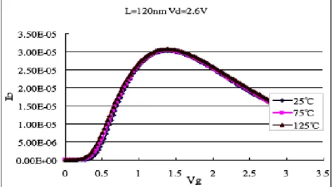
For 32A, 120nm input/output (I/O) devices, Figs. 1-3 show the experimental substrate currents versus Vg at room and elevated temperatures for three different drain voltages. When Vd = 2.2 V, a higher temperature causes a higher Ib. However,
when Vd = 3.0 V, a higher temperature causes a lower Ib. At Vd = 2.6 V, substrate
currents are almost independent of temperature. This voltage can be thus defined as the transition point. The behavior of Ib versus Vg at different temperatures is
consistent with the findings of the previous studies [5][6].
As for the drain current degradation, Fig. 4 shows an example of the stress bias set higher than the transition voltage (2.6 V). It is clear that Fig. 4 shows no reverse temperature effect. The degradation of drain current at room temperature is still more serious than the degradations of higher temperatures. The velocity saturation length effect is not shown here [3][4]. In fact, not only on Id,sat, Fig. 5
47
the worst case for digital circuit considerations. Also note that the trends in Fig. 5 clearly indicate that the room temperature situation is the most aggravated condition.
In the case of the drain bias set lower than the transition voltage, Fig. 6 still shows no reverse temperature effect at Vd = 2.2 V, in contradiction to a higher
temperature possessing a higher Ib. In addition, room temperature still reveals the
largest degradation among different temperatures for three types of drain current
!
as revealed in Fig. 7. Again, Id.op is still the worst case among the three currents
and Id.lin is worse than Id,sat.
Actually, in the case of the drain bias set at the transition voltage, i.e., Vd =
2.6 V, the results are the same as above.
4.2.2 Core devices
For 20A˚, 90 nm core devices, Fig. 8 shows the experimental substrate currents versus Vg at room and elevated temperatures for Vd = 2.2 V. Here, a
higher temperature causes a higher Ib. In fact, for Vd = 1.8 and 2.0V experiments, a
higher temperature also causes a higher Ib, and the waveforms of Ib are very
similar. No further higher Vd was tested in order to avoid inducing oxide
= 2.2 V, and the reverse temperature effect is consistent with previous findings of Aminzadeh and Wang [5][6].
Figure 9 shows the experimental Id,sat degradation versus stress time at
different temperatures stressed at Vd = 2.2 V. As expected, the degradations
increased as temperature rose from 25 to 125oC due to the reverse temperature effect. Figure 10 shows the degradation ratios of drain currents at different temperatures. Among them, the degradation of Id.op at 125oC is the worst case. For
digital circuits, Id.lin is worse than Id,sat.
4.3 Discussion and Conclusions
Although further studies spanning other nodes of technologies and sizes are required, the study at least shows the complicated nature of hot-carrier effects. The significant facts revealed here are (1) Ib commonly accepted as the parameter for
monitoring the drain avalanche hot carrier (DAHC) effect [7][8] needs to be modified since Id degradation and Ib variations versus temperature have different
trends as shown for I/O devices here. This may be attributed to some holes flowing to the gate oxide through the velocity saturation region, as was suggested by Koike
49
formulation considering all holes of impact ionization flowing to the substrate [10] may not reflect all the facts. However, if this problem is intended to be completely solved, the question that needs to be dealt with is how the impact ionization and two-dimensional electric field in the velocity saturation region are affected by temperature and drain voltage variations. (2) In this paper, we show that, using 32A˚ I/O devices of 0.13um technology as an example, the hot-carrier degradation of Id.op at room temperature is the worst case for temperature varying from 25oC to
an elevated value of 125oC and among Id.op, Id,sat and Id.lin, regardless of the
existence of the reverse temperature effect. (3) For the devices having a gate oxide thinner than 20A˚ , the transition points are high above the operational voltages and approach the edges of breakdown. Hence, the worst condition in considering hot-carrier reliability should be placed at elevated temperatures.
51
53
Fig. 4: △Id,sat versus stress time at Vd = 3.0 V with different temperatures.
55
Fig. 5: Drain current versus temperature at Vd = 3.0 V after stress 5000 seconds.
Fig. 6: △Id,op versus stress time at Vd = 2.2 V with different temperature.
57
Fig. 7: Drain current degradation versus temperature at Vd = 2.2 V after stress 5000 seconds.
59
Fig. 9: △Id,sat versus stress time at Vd = 2.2 V with different temperatures.
Fig. 10: Drain current degradation versus temperature at Vd = 2.2 V after stress 5000 seconds.
61
Chapter 5
An Investigation on Hot Carrier Effect at Elevated
Temperatures for pMOSFETs of 0.13 um Technology
5.1 Introduction
In the past few decades, the mechanism responsible for the hot carrier degradation in nMOSFET is believed to be the interface-state generation and the damage of gate oxide [1]. However, the situation for pMOSFET is less clear and had been long believed that hot carrier degradation of pMOSFETs is not so serious as nMOSFETs’ for the following reason. The mean free path of holes in silicon is about one half that of the electron [2]; therefore, holes scatter more frequently and fewer of them can reach enough high energy (about 4 eV) to create interface states [3]. But recent studies showed that even the transistor channel length has been scaled down into the deep-submicron regime (and supply voltages have been reduced) hot carrier induced degradation of pMOSFET has surprisingly become larger and approaching that of nMOSFET [4].
As to the temperature effects, in hot carrier conventional degradation concepts, operation at low temperature is more severe than at high temperature. However, recently study reveals that, operation at high temperature, the degradation is more severe than at room temperature [5], and the mechanism is
relative to NBTI (Negative Bias Temperature Instability) effect [6].
In this research, we studied two devices with different biases and temperatures to verify the mechanism and temperature effect on pMOSFETs. We found that the hot carrier degradation of Id,op (defined based on analog application)
is the worst in comparison with Id,lin and Id,sat. This message should be important
for designing analog circuits with satisfactory reliability. In addition, we found that the worst stress condition of 0.13µm technology and smaller is switched to the maximal gate voltage at high temperature.
5.2 Hot carrier of PMOSFETs and relative issues
5.2.1 PMOS Consideration
The carrier mobility of holes in silicon is about 470 cm2/V-s, and the mean free path is about one halt that of the electrons, hence, holes scatter more frequently and fewer of them reach high enough energies to create interface states. However, as the channel length has been scaled down into nano regime, hot carrier induced degradation of pMOSFETs has been approaching of nMOSFETs. For this
63
[12][13]. The details will discuss in following section.
5.2.2 Mechanisms
There have been lots of studies [5][14-17] on electron traps mainly utilizing an avalanche injection method. Electron trapping near the drain region leads to a reduction in threshold voltage and to the effective channel shortening. As a result, pMOSFETs drive current, transconductance and △Vt increase. However, this
mechanism is most important in longer channel pMOSFETs, and gate current IG
has been used as a predictor of the device lifetime [1]. As compared with electrons, holes are much less likely to be injected into an oxide, mainly due to the larger interfacial barrier height, however, once injected, they have much more influence on the MOSFET characteristics. It’s commonly believed that hole trapping centers originate from excess silicon and strained Si-O bonds near the Si-SiO2 interface
[7]. According to the experimental result [18] that hole traps are more difficult to be recovered than electron traps.
Another mechanism is interface state generation; it’s commonly believed to originate from silicon dangling bonds and oxygen dangling bonds, which are created by breaking originally inactive bonds. There are two kinds of mechanisms for interface state generation [7].
(1) The hydrogen model [14] suggests that a hydrogen-related center at the Si-SiO2 interface captures an incident carrier. This breaks the ≣Si-H or
≣Si-O-H bond, allowing the hydrogen-containing species to escape [7]. The broken-bond model suggests that a strained Si-O or Si-Si bond is broken by capturing an incident carrier, especially a hole, leading to structural modifications.
5.3 Experimental Results and Discussion
For 90 nm devices, Fig. 1, 2 and 3 show the experimental results of Id,lin, Id,sat and Id,op degradation versus stress time at different temperatures for stressed at Vd = -2.0V. As expected in [5], the degradations are increased as temperature rise from 25 ℃ to 125 ℃.
Fig. 4 shows the degradation ratios of drain currents with different temperatures. Among three temperatures, 125 ℃ is the worst case for core devices. The degradation of Id,op at 125 ℃ is worse than Id,lin and Id,sat, and for digital circuits, Id,sat is worse than Id,lin.
65
more severe degradation than higher temperatures, which obey the historical theory.
Fig. 8 shows the degradation ratios of drain currents versus different temperatures. Comparing those results, the degradation of Id,op is still the largest among all temperature range. Id,sat is the worst case for digital circuit considerations. This result follows the conventional concept that high temperature results in phonon scattering, which then reduces the drain current and impact ionization.
For CHC stress method, the stress bias Vg is set at -3.2V, and obviously, in Fig. 9, 10 and 11 show the results of d Id,lin, Id,sat and Id,op at 75℃ reveals more degradation than other temperatures. And the stress method of Vg=Vd, which causes more severe degradation rate more than Vg =Ib,max.
Fig. 12 shows the degradation ratios of drain currents versus different temperatures. Comparing those data, the degradation of Id,op is still the largest among all temperature range. And for digital circuit considerations, Id,sat is the worst case.
In order to find out the inside mechanism, Vt,lin shift is plotted in log-log scale as in Fig. 13. All curves in the Fig. 13 exhibit rather parallel trend and obey the power law as n lin t
At
V
=
∆
, (4-1)with n≈0.26 and A is a constant to be determine. We have examined the power law behaviors of △Vt,lin on DAHC and CHC stress modes for I/O devices and obtained exponent n≈0.6 and 0.4 in Fig. 14, 15 respectively. Because n≈0.25
is the typical trend of NBTI effect, we are then safe to say NBTI plus CHC would
make the worst stress mode for small scale pMOSFET. In addition, it is known that ∆Vt,lin only concerns with generated interface states’
charges q∆Nit and generated oxide trapped charges, q∆Not. But, if ∆Not’ effect is negligible, we will have [7]
∆
N
it∝
∆
V
t,lin∝
I
d,lindeg
radation
(4-2)Hence, as shown in Fig. 16, Id,lin degradation of core devices in log-log scale exhibits almost the same power law dependent and exponent n≈0.26. We can thus infer that generated oxide trapped charges must be minor in quantity and are negligible. The generated interface states are the dominant mechanism for all the degradation.
5.4 Conclusions
67
consideration, Id,sat is worse than Id,lin. We find temperature now has dominant effect on deciding the worst stress condition as the voltage did. (2) For I/O devices, we also found that the stress method with Vg=Vd is the
worst case. On the contrary, the hot carrier degradation of Id,op is the worst case at room temperature.
(3) For the hot carrier mechanism, it is found that the worst case of HC induced degradation on pMOSFETs has switched from low temperature to high temperature and from DAHC stress mode to CHC mode. Additionally, the severity of degradation on pMOSFETs has become comparable to their nMOSFET counterparts. By analysis the measured I-V data and power law behaviors, the switching can be presumed by the integration of HC and negative bias temperature instability (NBTI) effects, in which the generation of interface states plays the major role in damaging the pMOSFETs devices.
Leff = 90 nm Leff = 120 nm Vg Vd Vg Vd Id,lin -1.2 -0.05 -1.8 -0.05 Digital Id,sa -1.2 -1.2 -1.8 -1.8 Analog Id,op -0.53 -0.6 -0.68 -0.9
69 Length= 90 nm Vd=-2.0V -7% -6% -5% -4% -3% -2% -1% 0% 1 10 100 1000 10000 stress time (s) △ Id, lin 25℃ 75℃ 125℃
-8.0% -7.0% -6.0% -5.0% -4.0% -3.0% -2.0% -1.0% 0.0% 1 10 100 1000 10000 25℃ 75℃ 125℃ △I d ,s at stress time (s) Length=90 nm Vd= -2.0 V
71 -25.0% -20.0% -15.0% -10.0% -5.0% 0.0% 1 10 100 1000 10000 25℃ 75℃ 125℃ △I d, o p stress time (s) Length= 90 nm Vd=-2.0V
L=90nm Vd= -2.0V stress time=3000s 0% 5% 10% 15% 20% 25% 0 25 50 75 100 125 150 Temperature (℃) de gr ada ti on Id,lin Id,sat Id,op
Fig. 4. Drain current degradation versus temperature at Vd = -2.0 V after stress 3000 seconds.
73 Length=0.12um Vd=-3.2V -7% -6% -5% -4% -3% -2% -1% 0% 1 10 100 1000 10000 stress time (s) △ Id ,lin 25℃ 75℃ 125℃
-8.0% -7.0% -6.0% -5.0% -4.0% -3.0% -2.0% -1.0% 0.0% 1 10 100 1000 10000 25℃ 75℃ 125℃ △I d, sa t stress time (s) Length=0.12um Vd=-3.2V
75 -35.0% -30.0% -25.0% -20.0% -15.0% -10.0% -5.0% 0.0% 1 10 100 1000 10000 25℃ 75℃ 125℃ △I d ,o p stress time (s) Length=0.12um Vd=-3.2V
Fig. 8. Drain current degradation versus temperature at Vd = -3.2 V after stress 3000 seconds. L=120nm Vd= -3.2V stress time=3000s 0% 5% 10% 15% 20% 25% 30% 35% 0 25 50 75 100 125 150 Temperature (℃) degr adat io n Id,lin Id,sat Id,op
77 Length=0.12um Vd=-3.2V -18% -16% -14% -12% -10% -8% -6% -4% -2% 0% 1 10 100 1000 10000 stress time (s) △I d, lin 25℃ 75℃ 125℃
-25.0% -20.0% -15.0% -10.0% -5.0% 0.0% 1 10 100 1000 10000 25℃ 75℃ 125℃ △Id ,s at stress time (s) Length=0.12um Vd=-3.2V
79 -80.0% -70.0% -60.0% -50.0% -40.0% -30.0% -20.0% -10.0% 0.0% 1 10 100 1000 10000 25℃ 75℃ 125℃ △Id ,o p stress time (s) Length=0.12um Vd=-3.2V
L=120nm Vd= -3.2V stress time=3000s 0% 10% 20% 30% 40% 50% 60% 70% 80% 0 25 50 75 100 125 150 Temperature (℃) de g radat io n Id,lin Id,sat Id,op
81
Fig. 13.Vt,lin shift of core devices versus stress time.
CHC stress, Core decice, Vt,lin
0.001 0.01 0.1 1 10 100 1000 10000 Stress Time (s) V t,l in s hif t ( V ) 25℃-2.0V 25℃-2.2V 25℃-2.4V 75℃-2.0V 75℃-2.2V 75℃-2.4V 125℃-2.0V 125℃-2.2V 125℃-2.4V
Fig. 14.Vt,lin shift of I/O devices (DAHC) versus stress time.