A Broadband Noise-Canceling CMOS LNA for 3.1–10.6-GHz UWB Receiver
Chih-Fan Liao and Shen-Iuan Liu
Graduate Institute of Electronics Engineering & Department of Electrical Engineering National Taiwan University, Taipei, Taiwan 10617, R. O. C.
Abstract
An ultra-wideband (UWB) noise-canceling low-noise amplifier (LNA) is presented. By using inductive series and shunt peaking techniques, the effective bandwidth of noise canceling is extended. This LNA has been fabricated in a 0.18μm CMOS process. The measured noise figure is 4.5–5.1dB over 3.1–10.6-GHz, while the power gain is 9.7dB with a –3-dB bandwidth of 1.2–11.9-GHz. It consumes 20mW from a 1.8V supply and occupies only 0.59mm2.
I. Introduction
The demand for high-speed wireless communication systems is growing during the last few years. With a frequency spectrum allocated from 3.1 to 10.6-GHz, ultra-wideband (UWB) is emerging as a very attractive solution for short-distance and high data rate wireless communications. Two possible approaches have been proposed to implement an UWB system. One uses the multi-band OFDM modulation, while the other transmits short pulses with position or polarity modulation. Although the standard has not been completed, a front-end wideband low noise amplifier is indispensable regardless of the receiver architecture. The amplifier must meet several stringent requirements. Those include broadband input matching to minimize return loss, sufficient gain to suppress the noise of a mixer, low noise figure (NF) to enhance receiver sensitivity, low power consumption to increase battery life, and small die area to reduce the cost.
There are several existing solutions for high frequency wideband amplifiers in CMOS technology. Distributed amplifiers can bring the gain-bandwidth-product (GBW) to a value close to device fT, but consume large power and area [1]. Amplifiers employing shunt-shunt feedback are well-known for their wideband matching capability, but require high power consumption to obtain reasonable noise figure [2]. A multi-section LC ladder matching network has been proposed to achieve wideband matching, low noise figure, and low power consumption simultaneously [3]. However, the rapid growth of noise figure at high frequencies decreases the receiver sensitivity when operating at upper bands. Besides, the loss of inductors in the matching network contributes substantial noise, and this makes it difficult to realize them in a small area. In this work, the concept of noise canceling is re-exploited [4]. By using inductive series and shunt peaking techniques and the design methodology described in this paper, broadband noise canceling effectively lowers the noise figure over the target band under reasonable power consumption and small die area.
II. Circuit Description
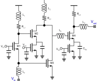
The proposed noise-canceling LNA is shown in Fig. 1.
The input stage incorporates a common-gate topology to facilitate ease of matching. Inductor L0 and parasitic capacitance of M1 and M3 form an LC ladder structure. The noise of M1 is canceled by M2 and M3. The bias of M3 is given by an off-chip RF choke, which also provides the dc current path of M1, and is not shown here for simplicity. Noise current due to M1 flows in opposite directions when combined at the drain of M2 and M3, while the signal currents will be added in phase. Inductors L1, L2, and L3 are added to extend circuit bandwidth and can be implemented with narrow traces to save area [5]. An output matching stage is cascaded for testing requirements. Transistor M4, with its source connected to a current source and a capacitor Chp, forms a high-pass gm stage. It
filters out low frequency components below 3-GHz, and makes the total circuit to exhibit a band-pass frequency response.
Fig. 1 Proposed broadband noise-canceling LNA.
The overall performance of this circuit lies on the design of the first two stages. The size and bias of M1, M2, and M3, together with the components value of RL1, L0, and L1, determine the effect of noise canceling and hence
the noise figure of this LNA. The following paragraphs describe how to optimize these parameters.
Fig. 2 shows the equivalent circuit for canceling of M1’s noise. The capacitor connected to the source of M2 is chosen to be roughly 4pF. It is viewed as a short over the desired band. The input and output are ac-shorted to ground when examining the effect of noise canceling. At low frequencies, the noise current In,out due to M1 can be
expressed as the following:
(
m L m S)
S m M n out ng
R
g
R
R
g
I
I
2 1 3 1 1 , ,1
+
−
=
(1)8-5-1
IEEE 2005 CUSTOM INTEGRATED CIRCUITS CONFERENCE
For In,out/In,M1=0, which results in successful noise
canceling, eq. (2) must be satisfied.
S m L
m
R
g
R
g
2 1=
3 (2) After noise canceling, the noise figure is then dominant by RL1, M2, and M3. The following equations describe how they contribute to the overall noise figure. The input matching condition RS=1/gm1 and eq. (2) areassumed through the derivations.
(
3 2 1)
2 1 2 2 1/
4
1 L S S L m m S m L RR
R
R
R
g
g
kTR
g
kTR
NF
L=
+
=
(3)(
3 2 1)
2 1 2 1 2 21
/
/
4
L m L S S L m m S m MR
g
R
R
R
R
g
g
kTR
kTg
NF
α
γ
α
γ
=
+
=
(4)(
m m L S)
m S S m MR
g
R
R
g
g
kTR
kTg
NF
3 2 1 2 3 3 31
/
/
4
α
γ
α
γ
=
+
=
(5)Thus, the total noise figure can be approximated as
S m L m L S
R
g
R
g
R
R
NF
3 1 2 11
1
1
1
α
γ
α
γ
+
⎟⎟⎠
⎞
⎜⎜⎝
⎛
+
+
=
(6)From eq. (6), in order to minimize noise contribution from M2 and RL1, the value of RL1 should be maximized. To obtain a flat gain response up to 10GHz, smaller size of M1 is then desirable to minimize its parasitic capacitance. Considering the 50ohm matching condition, the width and bias current of M1 are chosen to be 30μm and 2.5mA, respectively. By using inductive shunt peaking, the value of RL1 is constrained to voltage headroom, not bandwidth. It
heavily depends on the gate bias of M3. Though higher overdrive voltage makes fT higher, it drives MOS transistor
into velocity saturation region and makes its noise performance worse. Assuming an overdrive voltage around 150–200mV for M3, the value of RL1 is limited to 180ohm.
Fig. 2 Equivalent circuit for canceling of M1’s noise.
From eq. (2), it is now intuitive to choose M2 as a smaller device and M3 as a larger one. Actually, the size of M2 is chosen considering the trade-off between its parasitic loading on node Y in Fig. 2 and its noise performance. Similarly, wideband input matching sets an upper limit on the size of M3, while voltage headroom and noise contribution set the lower limit. Inductor L0 and
capacitance C0 form an LC ladder structure. When
terminated with resistive termination like 1/gm1, this structure can effectively match to 50ohm over a wide frequency range. The value of L0 is thus chosen to yield an
input impedance of roughly 50ohm and a high cut-off frequency, while inductor L1 is chosen according to bandwidth optimization. With a total power budget of 20mW, the only problem now remains to the choice of bias currents of M2 and M3.
The noise canceling condition governed by eq. (2) is not sufficient, since the impedance seen at node X (ZS) and
that seen at node Y (ZL) depend strongly on frequency. This
requires extensive simulations to determine the optimized ratio of gm3 to gm2. Fig. 3 shows the In,out/In,M1 ratio with
different ratios of gm3 to gm2. 2 4 6 8 10 12 0.0 0.1 0.2 0.3 0.4 0.5 0.6 0.7 In,out /In,M 1 Frequency (GHz) gm3 : gm2 3.8:1 4.5:1 5.9:1
Fig. 3 Simulated In,out/In,M1 with different values of gm3/gm2.
It can be seen that the optimized value is not equal to RL1/RS due to the frequency dependent nature of ZL and ZS.
Parasitic capacitance C0 and C1 cause impedance to roll off at high frequencies, and have been compensated by series inductor L0 and shunt inductor L1, respectively. The series
and shunt peaking techniques combined with gm3/gm2= 4.5
yield broadband noise canceling from 4 to 8-GHz. Since the noise power is of primary concern, an In,out/In,M1 ratio of
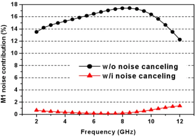
0.3 means that the noise power of M1 is attenuated by a factor larger than 10 when transferring to output. To further confirm the effect of noise canceling, M3 is turned off and Vb1 is lowered accordingly to emulate the condition without noise canceling. The percentage of M1’s noise contributed to total output noise is simulated and compared with the case with noise canceling. As shown in Fig. 4, applying noise canceling substantially lowers noise contribution of the matching device, since it not only cancels noise but also amplifies the signal.
S parameters and noise figure of this LNA are simulated by Cadence SpectreRF as shown in Fig. 5.
8-5-2
2 4 6 8 10 12 0 2 4 6 8 10 12 14 16 18 M 1 no is e con tri bu tion (% ) Frequency (GHz)
w/o noise canceling w/i noise canceling
Fig. 4 Simulated noise contribution of M1 with and without noise canceling.
In Fig. 1, due to the large drain to substrate capacitance introduced by M2 and M3 and loading of the last stage, inductors L2 and L3 are used to ameliorate the parasitic
capacitance [5]. The output stage is intended for 50ohm matching. When used in an integrated receiver, resistor RL3
and inductor L4 can be replaced with switching quad to form a single-balanced mixer. Typical loading of I/Q mixers on an LNA is thus considered in this design. The last stage consumes 5mA and has 4dB loss due to the 25ohm paralleled resistance. The simulated power gain is 10dB, and average noise figure over the target band is 3.9dB. Both S11 and S22 are below –10dB up to 11-GHz as shown in Fig. 5. 0 2 4 6 8 10 12 14 16 -35 -30 -25 -20 -15 -10 -5 0 5 10 15 0 2 4 6 8 10 12 14 160 1 2 3 4 5 S11 S22 S21 S 21, S11, S 22 (dB ) Frequency (GHz) NF NF ( d B)
Fig. 5 Simulated S parameters and noise figure.
III. Experiment Results
A microphotograph of this LNA is shown in Fig. 6. The circuit has been fabricated in a 0.18μm CMOS process and occupies an area of 0.9mmx0.65mm including pads. Measurements have been carried out on wafer.
S parameters and NF are measured using an ATN NP5B measurement system. Fig. 7 shows the measured power gain and output return loss. Measured power gain achieves a maximum of 9.7dB at 4.2-GHz, and remains 1-dB flatness from 2.4 to 9.4-GHz. It also exhibits a 3-dB bandwidth of 1.2–11.9-GHz. The discrepancy between measurement and simulation at high frequencies mainly
attributes to insufficient accuracy of inductor and transistor modeling. The measured output return loss is larger than 10dB up to 14-GHz. It shows different trend at low frequencies compared with simulation. This is due to process variation and the limited frequency range (1–18-GHz) of tuners used for noise measurement in this test plan. The measured input return loss and reverse isolation are shown in Fig. 8. S11 is below –10dB up to 14-GHz, while S12 is below –35dB across the band.
Fig. 6 Microphotograph of the LNA.
0 2 4 6 8 10 12 14 16 -25 -20 -15 -10 -5 0 5 10 15 S21 S22 S 21, S 22 (d B ) Frequency (GHz)
Fig. 7 Measured power gain and output return loss.
0 2 4 6 8 10 12 14 16 -45 -40 -35 -30 -25 -20 -15 -10 -5 S11 S12 S 11, S 12 (d B ) Frequency (GHz)
Fig. 8 Measured reverse isolation and input return loss.
2 4 6 8 10 12 3 4 5 6 7 8 9 10 NF ( d B ) Frequency (GHz)
Fig. 9 Measured and simulated noise figures (NFs). -Δ-: simulated NF without noise canceling -□-: simulated NF with noise canceling -●-: measured NF
The measured noise figure is illustrated in Fig. 9 and simulated ones are included for comparisons. Measurement shows a noise figure of 4.5–5.1dB over 3.1–10.6-GHz, and the average value is 4.7dB. A slight discrepancy of 0.5–1dB is observed between simulation and measurement. This is mainly caused by the lack of noise model of deep submicron CMOS. However, the effect of broadband noise canceling can be confirmed both in simulation and measurement.
Fig. 10 shows the measured IIP3 at 6-GHz. Applying two tones with 1-MHz spacing, the measured IIP3 is –6.2dBm, while P1dB is found to be –16dBm.
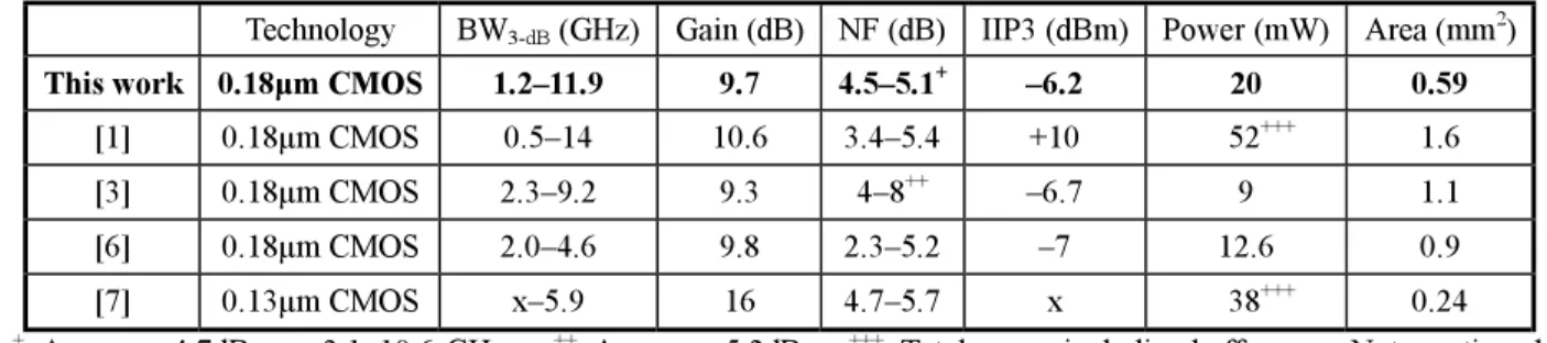
Performance summary of this LNA is listed in Table I. Other previously published LNAs, especially those for UWB systems, are included for comparisons. This work benefits from high bandwidth, low average NF, and small die area with moderate power consumption.
IV. Conclusion
A broadband noise-canceling LNA for a 3.1–10.6-GHz UWB receiver is implemented in 0.18μm CMOS technology. The proposed circuit achieves a power gain of 9.7dB, a 3-dB bandwidth of 1.2–11.9-GHz, an average noise figure of 4.7dB over the target band, and an input matching better than –10dB up to 14-GHz. It also occupies a small area of 0.59mm2 and consumes 20mW from a 1.8V supply. -40 -35 -30 -25 -20 -15 -10 -5 -100 -80 -60 -40 -20 0 IIP3= -6.2dBm Fundamental tone IM3 tone O u tpu t P o w e r (d B m ) Input Power (dBm)
Fig. 10 Measured IIP3 at 6-GHz.
Acknowledgement
This work was supported in part by MediaTek Inc. and National Science Council, Taiwan. The authors would like to thank National Nano Device Laboratory for measurement support and CIC for chip fabrication.
References
[1] R. Liu, C. Lin, K. Deng, and H. Wang, "A 0.5–14-GHz 10.6-dB CMOS cascode distributed amplifier," Symp. VLSI Circuits Dig. 17, pp. 139 - 140, June 2003.
[2] S. Andersson, C. Svensson, and O. Drugge, "Wideband LNA for a multistandard wireless receiver in 0.18 µm CMOS," Proceedings of the 29th European Solid-State Circuits Conference, pp. 655 - 658, Sept. 2003.
[3] A. Bevilacqua and A. M. Niknejad, "An ultra-wideband CMOS LNA for 3.1 to 10.6GHz wireless receivers," IEEE International Solid-State Circuits Conference, vol. XVII, pp. 382 - 383, Feb. 2004.
[4] F. Bruccoleri, E. A. M. Klumperink, and B. Nauta, "Noise canceling in wideband CMOS LNAs," IEEE International Solid-State Circuits Conference, vol. XLV, pp. 406 - 407, Feb. 2002.
[5] T. H. Lee, The Design of CMOS Radio-Frequency Integrated Circuits, 1st ed., New York: Cambridge Univ. Press, 1998.
[6] C.-W. Kim, M.-S. Kang, P. T. Anh, H.-T. Kim, and S.-G. Lee, “An Ultra-Wideband CMOS Low Noise Amplifier for 3–5-GHz UWB System,” IEEE Journal of Solid-State Circuits, vol. 40, pp. 544 - 547, Feb. 2005.
[7] R. Gharpurey, "A broadband low-noise front-end amplifier for ultra wideband in 0.13µm CMOS," 2004 IEEE Custom Integrated Circuits Conference, May 2004. Table I. Performance Summary
Technology BW3-dB (GHz) Gain (dB) NF (dB) IIP3 (dBm) Power (mW) Area (mm2)
This work 0.18μm CMOS 1.2–11.9 9.7 4.5–5.1+ –6.2 20 0.59 [1] 0.18μm CMOS 0.5–14 10.6 3.4–5.4 +10 52+++ 1.6
[3] 0.18μm CMOS 2.3–9.2 9.3 4–8++ –6.7 9 1.1
[6] 0.18μm CMOS 2.0–4.6 9.8 2.3–5.2 –7 12.6 0.9 [7] 0.13μm CMOS x–5.9 16 4.7–5.7 x 38+++ 0.24
+: Average= 4.7dB over 3.1–10.6-GHz ++: Average= 5.2dB +++: Total power including buffer x: Not mentioned