208 IEEE ELECTRON DEVICE LETTERS, VOL. 17, NO. 5, MAY 1996
Enhanced Electron Emission from Phos
Doped Diamond-Clad Silicon Field Emitter Arrays
T. K. Ku, S.
H.
Chen, C .D.
Yang,N.
J.
She, C. C.
Wang,C.
F.
Chen,I. J.
Hsieh,and H.
C.
Cheng
Abstract-Undoped and phosphorus (P)-doped diamond-clad Si field emitter arrays have been successfully fabricated using mi- crowave plasma chemical vapor deposition (MPCVD) technology. The electron emission from the blunt diamond-clad microtips are much higher than those for the pure Si tips with sharp curvature due to a lower work function. Furthermore, the characteristics of emission current against applied voltage for the P-doped diamond-clad tips show superior emission at lower field to the un- doped ones. After the examination of Auger electron spectroscopy (AES) and electrical characteristics of as-grown diamond, such a significant enhancement of the electron emission from the P-doped diamond-clad tips is attributed to a higher electron conductivity and defect densities.
I. INTRODUCTION
IAMOND has recently been considered as the most appropriate and promising cold-cathode material for vac- uum microelectronic devices due to its several important advantages. (1) The (1 11) diamond has a negative or at least very small electron affinity [l]. (2) Diamond is well known to be one of the most chemically and physically stable material and simultaneously has the highest thermal conductivity
[2].
(3) High breakdown threshold and large high-field electron velocity of diamond enhance the maximum emission current limited by current saturation 121. Recently, several papers reported the electron emission from CVD-grown diamond films and Si tips coated with diamond particles at their apex end regions [3]-[7]. Our previous work further indicated that the diamond-clad tips show a much better electron emission capability as compared with pure Si and Cr-clad microtips and diamond films coated on plain substrates [8]. However, the doping of diamond is necessary since diamond itself is an excellent insulator. Generally, n-type doping is preferred over p-type for electron emission. However, the implementation of effective and reliable n-type dopants is still difficult. Up to date, only Okano et al. reported the electron emission from phosphorus (P)-doped diamond films on plain Si substrates, showing low-field emission as compared to boron (B)-doped films [9]. In this letter, P-doped diamond films on Si mi- crotips have been successfully fabricated by the microwave plasma chemical vapor deposition (MPCVD) technique and Manuscript received October 21, 1995; revised January 25, 1996. This work was supported by the Republic of China National Science Council under Contract no. NSC 84-2622-E-009.012.T. K. Ku, S. H. Chen, C. D. Yang, N. J. She, C. C. Wang, C. F. Chen, and H. C. Cheng are with National Chiao Tung University, Hsinchu, Taiwan, R.O.C.
I. J. Hsieh is with Chung-Hua Polytechnic Institute, Hsinchu, Taiwan, R.O.C.
Publisher Item Identifier S 0741-3 106(96)03730-5.
characterized. This is the first report on the electron emission characteristics of P-doped diamond-clad Si tips.
11. EXPERIMENTAL PROCEDURES
A 1 pm-thick oxide layer was grown and was photolitho- graphically patterned to form arrays of SO
x
SO circular discs 3 pm in diameter on 2 N 4 R-cm, (100)-oriented n-type Si substrates. Employing the previously patterned oxide layer as the mask, the cone-shaped Si microtip arrays were subsequently formed using SFG/Cl:, reactive ion etching [IO].
An oxidation-and-stripping process was applied to further sharpen the etched tip to about 250
8,
in radius [l I]. The aspect ratio of the resultant sharp silicon microtips is about 3 pm/3 pm. Before the deposition of diamond, the as-fabricated sharply curved Si microtips were first cleaned by H2 plasma pretreatment and followed by diamond powder (particle size, 0.1 pm) scratching. In order to growa
continuous diamondfilm, diamond powder scratching process is necessary to create nucleation sites on the surface of Si substrates. Then, the undoped diamond films were deposited on the 2
x
2 mm2 Si substrates with a 50 x 50 tips array using microwave plasma enhanced CVD at 850°C using a gaseous mixture of CH4 in CO2. The microwave power was set at 450 W and the reaction time was 2 h. The pressure during deposition was 25 Torr. For the P-doped diamond, the deposition conditions were the same as the undoped ones except that trimethyl phosphite (P(OCH3)s) was introduced as the doping reactant during diamond deposition [ 121.111. RESULTS AND DISCUSSION
In general, high-quality diamond films can be obtained by reducing the flow rate ratio of CH4/C02. However, perfect diamond is an excellent insulator which makes stable electron field emission impossible. According to our previous work and other works by Zhu et al. and Xu et al., the higher defect densities in CVD-grown diamond films are responsible for the enhanced electron emission [6],
[7].
Besides, the low flow rate ratio leads to a rough and nonuniform coating morphology on the high curvature tip region. Hence, the defective diamond crystallites deposited by a higher flow rate ratio of C H 4 / C 0 2 are preferred. The flow rate ratio of CH4/C02 consequently chosen was 68.4% ( 2 0 3 3 0 ) with 0.2 sccm P(OCH3)s dopant (or a P/C ratio of 3960 ppm) to achieve the defective P-doped diamond films. The SEM images shown in Fig. l(a) and (b) demonstrate the surface morphology of undoped and P-doped diamond-clad Si tips deposited by 68.4% CH4 in CO2 gaese mixture with a P/C ratio of 3960 ppm. To form a continuous 0741-3106/96$05.00 0 1996 IEEEKU et al.: PHOSPHORUS-DOPED DIAMOND-CLAD SILICON 500 0 -
E
-500?,
8
&
5
-1000 -1500 -2000 209-
-
-
-
-
1000 Diamond shoulder I , (a) (b)Fig. 1. The SEM images of diamond-clad Si tips deposited by 68.4% CHq
in CO2 gas mixture (a) the undoped diamond-clad Si tips (b) the P-doped diamond-clad Si tips deposited with the 0.2 sccm P(OCH3)n dopant (or a P/C ratio of 3960 ppm).
and uniform coating, a thicker film (-3 pm) was grown and therefore resulted in a much more blunt shape than the original un-coated Si tip. Moreover, the P-doped diamond-clad tips shown in Fig. 1 are slightly less in size uniformity compared to the undoped ones. This is due to the significantly decreased nucleation density for the P-doped diamond.
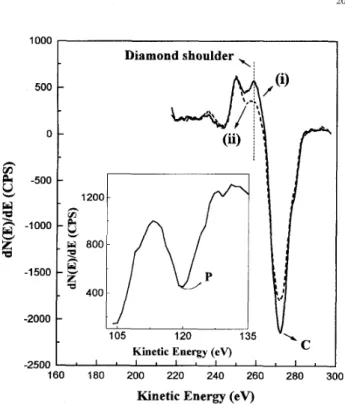
Auger electron spectroscopy (AES) was used to identify the surface compositions of the diamond-clad Si microtips. The AES spectra corresponding to the specimens in Fig. I(a) and (b) are shown in Fig. 2. In these spectra, the carbon peak at 272 eV was detected and neither Si nor 0 peaks were detected. The low-energy shoulder arround 260 eV in the positive peak of the carbon main peak existed in the undoped sample indicated that the surface structure was diamond rather than graphitic components [13]. However, the AES spectrum of P-
doped sample did not exhibit an obvious shoulder, implying a diamond-like carbon nature containing a large amount of graphitic, amorphous carbon and/or other defects. Moreover, the small insert in Fig. 2 indicates a successful P doping by detecting a phosphorus peak at around 120 eV. According to the detectable sensitivity of AES spectrum, the P concentration is high, in the order of lo1' cmP3.
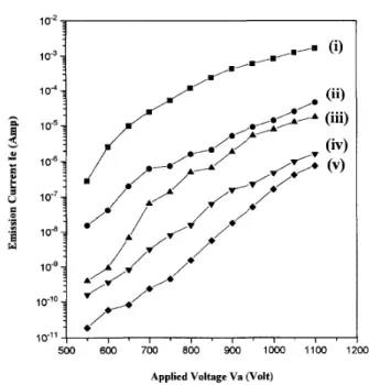
Field emission properties of the diamond-clad samples were characterized in high-vacuum environment with a base pressure of 2.5 x Torr. The spacing between the emitter and the graphite collector was controlled at a constant -30 pm and the tip number in an array was 50 x 50. When a copper plate instead of the tip array was put on the cathode, a current of less than 1 nA was measured. As shown in Fig. 3, the emission current (Ie) versus applied voltage (Va) characteristics of the P-doped and undoped diamond-clad microtips are both superior to that of pure Si microtips, in spite
of their relatively blunt curvatures. This may be attributed to the lowering of the work function due to the negative electron affinity of ( I 11) diamond films and/or the much larger effective emission area of the diamond coating. At Va = 1100 V, a much higher emission current (Ie) of 1.69 mA for the P-
-I ~ I
- 2 5 0 0 L ' 1 ' 1 ' ' ' 1 s 1 ~ ~ m
160 180 200 220 240 260 280 300
Kinetic Energy (eV)
Fig. 2. Auger electron spectra (AES) of (i) undoped diamond-clad Si tips and (ii) P-doped diamond-clad Si tips. The main carbon peak at 272 eV was detected and neither Si nor 0 peaks were detected. Moreover, the small insert indicates a successful phosphorus doping by detecting a phosphorus peak at around 120 eV.
doped diamond-clad emitters with 3960 ppm P/C ratio was achieved, compared to only 45 /LA from the undoped ones. Hence, the electron emission from the diamond-clad tips was greatly enhanced by introducing the P dopants. Defining FT as the threshold values of the applied field needed to generate a current of 20 pA in our array size with about 0.2 mm2 (i.e.,
a
typical current density of 10 mA/cm2 required for effectively exciting a phosphor pixel in a field emission diaplay), the FT value was reduced from 33.6 V/pm for the undoped diamond- clad tips to 22.3 V/pm for the P-doped ones. The resistivities of the P-doped diamond films were measured by the four-point probe method and were found at least one-order of magnitude lower than those of undoped films. It is believed that the P-dopants and their associated defect densities increase the energy state densities within the band gap of the diamond film[14]. Subsequently, it causes both a higher conductivity and the remarkable enhancement of the electron emission from the P-doped diamond-clad tips. To confirm that the emission was indeed field emission, the currents emitted from plain substrates coated with P-doped and undoped diamond layer were also investigated. The emission currents measured at Va = 1100 V were only about 17 pA for the former and 760 nA for the latter. This indicates that most of the emission currents are contributed from the diamond-clad tips.
IV. CONCLUSIONS
In summary, uniform and continuous diamond films have been successfully coated on Si microtips using the MPCVD technology. The characteristics of emission current against applied voltage for the blunt P-doped diamond-clad tips show
210 10“ 10“ 106 IO-’ 1 o4 104 10-10 /.’ 6’ 10-1‘
jl
.
I I I I I I I I I I I 500 600 700 800 900 loo0 1100 1Applied Voltage Va (Volt)
Fig. 3. Emission current (Ie) versus applied voltage (Va) characteristics of (i) the P-doped diamond-clad tips; (ii) undoped diamond-clad tips; (iii) the P-doped diamond-clad plain Si substrate; (iv) the sharp Si tips; (v) the undoped diamond-clad plain Si substrate. The spacing between the emitter and collector was a constant about 30 p m and the tip number in an array is 50 x 50.
superior emission at lower field to both the un-doped ones and sharp Si tips. By examining with Auger electron spectroscopy and by electrically characterizing the as-grown diamond, the significant enhancement of the electron emission from the P-
doped diamond-clad tips can be attributed to a higher electron conductivity and higher defect densities.
ACKNOWLEDGMENT
The authors acknowledge technique supports from the Na-
tional Nan0 Device Laboratory of NSC and Semiconductor Research Center of National Chiao-Tung University and thank
R. L. Huang for her valuable support in AES analysis.
IEEE ELECTRON DEVICE LETTERS, VOL. 17, NO. 5 , MAY 1996
REFERENCES
[1] F. J. Himpsel, J. A. Knapp, J. A. Van Vechten, and D. E. Eastman, ”Quantum photoyield of diamond (1 1 1)-A stable negative-affinity sur- face,” Phys. Rev. B., vol. 20, p. 624, 1979.
[2] M. N. Yoder in Diamond and Diamond-Like Films and Coatings, R. E.
Clausing et ai., Ed.
[3] C. Wang, A. Garcia, D. C. Ingram, M. Lake, and M. E. Kordesch, “Cold field emission from CVD diamond films observed in emission electron microscopy,” Electron. Lett., vol. 27, p. 1459, 1991.
[4] E. I. Givargizov, V. V. Zhirnov, A. N. Stepanova, E. V. Rakova, A. N. Kiselev, and P. S. Piekhanov, “Microstructure and field emission of diamond particles on silicon tips,” Appl. Sur. Sci., vol. 87/88, p. 24,
1995.
[ 5 ] N. Liu, Z . Ma, X. Chu, and T. Hu, Z. Xue, X. Jiang, and S. Pang, “Fabrication of diamond tips by the microwave plasma chemical-vapor- deposition technique,” J. Vac. Sci. & Technol. B , vol. 12, p. 1712,
1994.
[6] W. Zhu, G. P. Kochanski, S. Jiu, L. Seibles, D. C. Jacobson, M.
McCormack, and A. E. White, “Electron field emission from ion- implanted diamond,” Appl. Phys. Lett., vol. 67, p. 1157, 1995. [7] N. S. Xu, R. V. Latham and Y. Tzeng, “Field-dependence of the area-
density of ‘cold’ electron emission sites on broad-area CVD diamond films,” Electron. Lett., vol. 29, p. 1596, 1993.
[8] H. C. Cheng, T. K. Ku, B. B. Hsieh, S. H. Chen, S. Y. Leu, C. C. Wang, C. F. Chen, I. J. Hsieh and C. M. Huang, “Fabrication and characterization of diamond-clad silicon field emitter arrays,” to be published in Jpn. J. Appl. Phys. Part A.
[9] K. Okano and K. K. Gleason, “Electron emission from phosphorus- and boron-doped polycrystalline diamond films,” Electron. Lett., vol. 3 1, p.
74, 1995.
[lo] T. K. Ku. M. S. Chen, C. C. Wang, W. F. Lee, M. S. Feng, I. J. Hsieh, C. M. Huang and H. C. Cheng, “Fabrication of gated field emitter arrays for vacuum microtriodes,” Proc. Int. Sym. Electron Device & Material,
Taiwan, 1994, pp. 1134-1136.
[ 111 R. B. Marcus, T. S. Ravi, T. Gmitter, K. Chin, W. J. Orvis, D. R. Ciarlo, C. E. Hunt and Trujillo, “Formation of silicon tips with
<
1 nm radius,”Appl. Phy. Lett., vol. 56, p. 236, 1990.
[ 121 S. H. Chen, S. L. Chen, S. F. Lo, and C. F. Chen, “The synthesis and characterization of phosphorus-doped diamond films using TriMethyl- Phosphite as a doping source,” to be published in Diamond and Relative
Materials.
[13] P. Sander, U. Kaiser, M. Altebockwinkel, L. Wiedmann, A. Ben- ninghoven, R. E. Sah and P. Koidl, “Depth profile analysis of hydro- genated carbon layers on silicon by x-ray photoelectron spectroscopy, Auger electron spectroscopy, electron energy-loss spectroscopy, and secondary ion mass spectrometry,” J , Vac. Sci. Technol. A, vol. 5, p.
1470. 1987.
[14] G. B. Bachelet, G. A. Baraff, and M. Schluter, “Defects in dia- mond-The unrelaxed vacancy and substitutional nitrogen,” Phys. Rev. B , vol. 47, p. 4736, 1981.