國 立 交 通 大 學
光 電 工 程 研 究 所
碩士論文
利用奈米圖型化基板製作高效率氮化鎵發光二極體
High efficiency GaN-based light emitting diodes grown on
nano-patterned substrates
研究生:詹宗穎
指導教授:郭浩中 教授
盧廷昌 教授
利用奈米圖型化基板製作高效率氮化鎵發光二極體
High efficiency GaN-based light emitting diodes grown on nano-patterned
substrates
研究生:詹宗穎 Student: Chung-Ying Chan 指導教授:郭浩中 教授 Advisor: Prof. Hao-Chung Kuo
盧廷昌 教授 Prof. Tien-Chang Lu
國 立 交 通 大 學 光電工程研究所
碩 士 論 文 A Thesis
Submitted to Institute of Electro-Optical Engineering College of Electrical Engineering
National Chiao Tung University in Partial Fulfillment of the Requirements
for the Degree of Master
In
Electro-Optical Engineering July 2010
利用奈米圖型化基板製作高效率氮化鎵發光二極體
研究生:詹宗穎 指導教授: 郭浩中教授
盧廷昌教授
國立交通大學光電工程研究所碩士班
摘要
在此論文當中,我們提出於氮化鎵與藍寶石基板接面製作二氧化矽
奈米柱陣列,以提高氮化鎵發光二極體發光效率。藉由穿透式電子顯微
鏡剖面圖可觀察到氮化鎵在側向成長過程中,氮化鎵與藍寶石基板接面
所形成的空氣洞以及氮化鎵中的 Stacking fault 有效地減少穿透缺陷
密度,此外我們分別從 X 光繞射及光激發量測從得知氮化鎵磊晶品質有
所改善,相較於傳統氮化鎵發光二極體,出光強度及內部量子效率都有
所提升,利用此方法可增加光萃取效率及改善氮化鎵磊晶品質。
論文第二部分中,我們展示利用具有二氧化矽側壁保護的氮化鎵奈
米柱陣列,製作出高品質及少量殘餘應力的兩吋獨立式氮化鎵基板,並
藉由側向成長機制將氮化鎵奈米柱彼此接合而形成氮化鎵薄膜,相較於
傳統氮化鎵發光二極體成長在藍寶石基板上,成長於獨立式氮化鎵基板
具有低穿透缺陷密度以及較好的散熱能力,此外,利用獨立式氮化鎵基
板可減少成長氮化鎵過程中應力的產生,並降低在變電流過程中電激發
頻譜峰值的藍移及效率遽降的現象,電激發內部量子效率有26.8%的增
益。
High efficiency GaN-based light emitting diodes grown on
nano-patterned substrates
Student : Chung-Ying Chan Advisor: Prof. Hao-Chung Kuo Prof. Tien-Chang Lu
Institute of Electro-Optical Engineering National Chiao Tung University
Abstract
In this thesis, we investigated high efficiency InGaN/GaN light emitting diodes (LEDs) grown on sapphire substrate with SiO2 nanorod-array (NRA). The transmission
electron microscopy images suggested that the voids between SiO2 nanorods and the
stacking faults introduced during the nanoscale epitaxial lateral overgrowth (NELO) of GaN can effectively reduce the threading dislocation density. The GaN film showed improvement in crystal quality through x-ray diffraction FWHM and photoluminescence measurement. The light output power and internal quantum efficiency of the fabricated LED were enhanced compared to those of conventional LED. The improvements could be attributed to both the enhanced light extraction by utilizing SiO2 NRA and the
improved crystal quality through the NELO method.
In the second part, we demonstrated a method for fabricating 2 in. freestanding GaN substrates of high crystallographic quality and low residual strain. Arrays of GaN
nanorods with SiO2-passivated sidewall were randomly fabricated on the sapphire
substrate as growth seeds. The SiO2-passivated sidewall prevents the coalescence of GaN
grains in spaces between the rods, causing them to grow preferentially on the top of individual rods. GaN LEDs grown on free-standing GaN substrate can reduce threading dislocation density and provide better thermal dissipation compared to that grown on sapphire substrate. Moreover, the reduction of strain by using free-standing GaN substrate results in smaller blue shift of current-dependent EL spectrum and efficiency droop. The EL IQE improvement of GaN-based LEDs grown on free-standing GaN was 26.8% .
致謝
轉眼間,兩年的碩士生活已到畢業的時刻,回想當初踏入實驗的緊張與惶恐, 如今我將帶著滿滿的不捨,離開奮鬥兩年的交大校園。首先,我要感謝郭浩中老師 在待人處事方面的開導,令我看到更為寬廣的世界,盧廷昌老師在研究上的熱誠也 是相當令人值得學習。 感謝清華學長在實驗方面的規劃與教導,學長總是不厭其煩給予我研究上的幫 助也不吝於給予知識的傳承,李博與鏡學學長在磊晶的全力 support,令我不禁想 和兩位學長來個充滿力量的擊拳,主立學長製程的能力相當令我敬佩,閔安學長光 學模擬的協助,感謝明華學長與輝閔學長的 CL 量測,此外要感謝的就是 LED team 的各位,與 Joseph 的討論與寶貴的意見,小昕與 David 量測方面的幫忙,小杜製程 方面的努力,以及許多學弟妹的協助,讓我得以順利完成碩士論文。此外,冷面笑 匠阿祥、很會帶氣氛的嗡嗡、割雙眼皮的哭哭、實驗室奇葩獸黃與小胖、很客氣的 依嚀、反應跳 tone 的小邱、一個月的 roommate 林詳淇、默默低調的永吉、話題一 直很多的彥群、年紀很大卻很幼稚的信助、愛找吃飯的板弟以及學弟妹的陪伴都使 得我的碩士生活豐富不少。 雖然在交大只有短短的兩年,但不論實驗研究上的歷練或是在實驗室中與各位 相處的愉快時光,相信都會在我人生當中寫下精彩的篇幅,祝各位在人生旅途中可 達到自己的期許。 最後,要感謝我的家人,有你們的支持我才能順利完成兩年的碩士生活,但願 你們能與我分享這份喜悅。Content
摘要………i Abstract………..iii 致謝………v Content………...vi List of Figures………..…viiiChapter1 Introduction
1-1 Development of Ⅲ-Nitride light emitting diodes (LEDs)……….11-2 Basic of Ⅲ-Nitride LEDs……….3
1-3 Properties of Ⅲ-Nitride LEDs………..5
1-4 Efficiency and improvement issue of Ⅲ-Nitride LEDs………6
1-4.1 Advantages of patterned sapphire substrate LEDs……….8
1-4.2 Comparision of Sapphire substrate and GaN substrate………10
Chapter2 Experimental instruments and methods
2-1 Scanning electron microscope-Cathodoluminescence (SEM-CL)………..…152-2 Atomic Force Microscopy(AFM)………15
2-3 X-ray diffraction (XRD)……….17
2-4 Raman spectroscopy………...19
2-5 Photoluminescence spectroscopy (PL)……….20
2-6 Electroluminescence spectroscopy (EL)……….21
Chapter3 InGaN/GaN LEDs grown on sapphire substrate with SiO
23-1 Process of depth dependent SiO2 NRA on sapphire substrate………..28
3-1.1 Nano-scale Ni mask………..28
3-1.2 Fabrication of SiO2 NRA on sapphire substrate………..29
3-2 InGaN/GaN LEDs grown on sapphire substrate with SiO2 NRA………30
3-2.1 Epitaxial characteristics of GaN film grown on sapphire substrate with SiO2 NRA………30
3-2.2 InGaN/GaN multiple quantum wells grown on sapphire substrate with SiO2 NRA………33
3-3 Measurement and discussion………33
3-3.1 Photoluminesence measurement………33
3-3.2 Electroluminesence measurement……….37
3-3.3 2-Dimension FDTD simulation………38
Chapter4 InGaN/GaN LEDs grown on free-standing GaN substrate
4-1 Process of free-standing GaN substrate………...484-1.1 Fabricaiton of GaN nanorods………...49
4-1.2 GaN nanorods self-separated Hydride vapor-phase epitaxy (HVPE)………49
4-1.3 Epitaxial characteristics of free-standing GaN substrate………..50
4-2 InGaN/GaN multiple quantum wells grown on free-standing GaN substrate……51
4-3 Measurement and discussion………...52
4-3.1 Raman spectrum………..…52
4-3.2 Electroluminesence measurement………..52
Chapter 5 Conclusions
………..………69List of figures
Fig. 1-1 The air/GaN interface and the totally internal reflect.
Fig. 1-2 Schematic illustration of increased light extraction efficiency Fig. 1-3 Top and cross-sectional view SEM images of a PSS by wet etching Fig. 1-4 SEM morphologies of PSS
Fig. 2-1 Schematic diagram of a scanning electron microscope Fig. 2-2 Ray diagram showing two basic operations of TEM Fig. 2-3 Bragg diffraction from a symmetric plane
Fig. 2-4 Bragg diffraction from an asymmetric plane
Fig. 2-5 Geometry for x-ray rocking curve. The angle movement for the detector is twice that of the sample
Fig. 2-6 Surface Raman scattering spectrum measured from the GaN epilayer at room temperature
Fig. 2-7 Atom vibration modes in hexagonal GaN with the c-axis upworad Fig. 2-8 Interband transitions in photoluminescence system
Fig. 2-9 Spectrum of a blue/green electroluminescent light source for a clock radio. Peak wavelength is at 492 nanometers and the FWHM spectral bandwidth is quite wide
at about 85 nm.
Fig. 3-1 Schematic illustrations of GaN LED grown on sapphire with SiO2 NRA process
flow chart
Fig. 3-2 The relationship of mean diameter and spacing of the formed Ni nano-cluster versus the RTA temperature
Fig. 3-3 The relationship of mean diameter and spacing of the formed Ni nano-cluster versus the Ni thickness
Fig. 3-4 SEM image of (a) the fabrication SiO2 NRA (b) GaN nuclei on the sapphire with
SiO2 NRA as growth seeds (c) the GaN epilayer on the sapphire with 100nm SiO2
NRA (d) 200nm SiO2 NRA (e) 300nm SiO2 NRA
Fig. 3-5 The TEM images of the GaN/sapphire interface for the GaN epilayer grown on (a) a planar sapphire substrate and (b) on sapphire with SiO2 NRA. The inset of (b)
shows the dislocation bending phenomenon with visible turning points.
Fig. 3-6 The schematics of (a) the overgrowth process and the formation of dislocations, stacking faults, and voids at the initial stage of epitaxy, and (b) three potential mechanisms accounted for the reduction of the TDD.
Fig. 3-7 XRD full-width at half- maximums (FWHMs) of the GaN films grown as a function of the SiO2 NRA depth
Fig. 3-8 The peak intensity of GaN divided by peak intensity of yellow band as a function of SiO2 NRA depth
Fig. 3-9 The schematic of InGaN/GaN LED structure
Fig. 3-10 IQE of GaN-based LEDs as a function of carrier density at 15K and 300 K Fig. 3-11 I-V curves of GaN-based LED grown on sapphire with and without SiO2 NRA
Fig. 3-12 I-V curves of GaN-based LED grown on sapphire with and without SiO2 NRA
Fig. 3-13 GaN-based LED structure for 2D FDTD simulation
Fig. 3-14 Enhancement in light output power as a function of SiO2 NRA depth
Fig. 4-1 Schematic illustrations of the fabrication of free-standing GaN substrate by nanorods assistance separation
Fig. 4-2 SEM image of GaN nanorods
Fig. 4-3 SEM image for GaN nanorods with sidewall passivation
Fig. 4-4 SEM images for the initial stage of HVPE regrowth with a growth time of 2min Fig. 4-5 SEM images of HVPE regrowth with a growth time of 5min
Fig. 4-6 TEM images of GaN substrate by nanorods assistance separation Fig. 4-7 CL images of GaN substrate by nanorods assistance separation
Fig. 4-8 Results of GaN thick films obtained from (a)GaN nanorod arrays and (b) flat GaN
Fig. 4-9 The schematic of GaN-based LED structure
Fig. 4-10 Raman analysis of GaN grown on sapphire and free-standing GaN
Fig. 4-11 L-I curves of GaN-based LED grown on sapphire substrate and free-standing GaN substrate
Fig. 4-12 I-V curves of GaN-based LED grown on sapphire substrate and free-standing GaN substrate
Fig. 4-13 The current dependent EL spectra of LED grown on (a) free-standing GaN substrate (b) sapphire substrate
Fig. 4-14 Blue-shift of peak wavelength as a function of injection current
Chapter 1
Introduction
1-1 Development of Ⅲ-Nitride light emitting diodes(LEDs)
In 1907, Henry Joseph Round demonstrated that light was emitted from a SiC crystallite as used for sandpaper abrasive. This is the first light emitting diodes (LEDs). He immediately reported his observations to the editor of the journal Electrical World [1]. In 1962, Nick Holonyak Jr. et al. used vapor-phase epitaxy (VPE) to fabricate GaAsP junctions on GaAs subtrates. They observed the emission of coherent visible light at low temperature. Then Nick Holonyak Jr. and S.F. Bevacqua had reported a GaAsP junctions which emitted coherent visible light in the first volume of Applied Physics Latter [2]. The publication marks the beginning of viable p-n junction LEDs emitting in the visible wavelength range. However, due to the lattice mismatch between the GaAsP epilayer and GaAs substrate resulted in a high density of dislocations. Therefore, the efficiency of GaAsP LEDs was quite low. In order to improve efficiency, the importance of the growth conditions and thickness of a buffer layer was realized by Nuese.
In 1967, Logan’s group demonstrated the GaP LEDs. These junctions were formed by growing an n-type GaP layer onto Zn-O-doped GaP wafers. In fact, GaP is an indirect gap semiconductor that does not emit significant amounts of light due to the requirement
of momentum conservation in optical transitions. If GaP was doped with an optically active isoelectronic impurity such as N or O, strong optical transitions were obtained. The optical transitions emitted in the red and green parts of spectrum.
The AlGaInP material system was developed in Japan in the early 1980s. AlGaInP material is suited for high brightness emission due to the lattice match with GaAs substrate. The emission range includes red (625nm), orange (610nm) and yellow (590nm). In 1997, further improvement was attained by using multiple quantum well (MQW) active regions that provided the effect of carrier confinement to increase the recombination probability of electron and hole. Also distributed Bragg reflectors and transparent GaP substrate technology could enhance light output. In 1999 chip shaping such as the truncated inverted pyramid (TIP) was employed to increase light brightness.
In 1992, the first GaN p-n homojunction LED was reported by Akasaki. The LED was grown on a sapphire (Al2O3) substrate by organometallic vapor-phase epitaxy
(MOCVD) and emitted light in the ultraviolet and blue spectral range. The efficiency was about 1%. In 1990s, Shuji Nakamura and his coworker which take office at Nichia Chemical Industries Corporation reported numerous research and contribution. They demonstrated the first blue and green GaInN/GaN double hetero juncution LED and the first pulsed and cw current injection blue laser operating at room temperature.
The GaN based blue LEDs development had been attracted for the number of illumination application. The white LEDs was a very interesting part of them. There were several ways to generate the white light with LEDs. The creation of white light could base on dichromatic or trichromatic approaches with blue, red and green LEDs. By another way, the generation of white light could base on phosphors excited by GaN-based blue or ultraviolet LEDs.
1-2 Basic of Ⅲ-Nitride LEDs
The brightest devices use either a single or multiple quantum well structure. A typical complete device structure is consist of a low-temperature deposited GaN or AIN buffer layer on c-plane sapphire, a 3-4 um silicon-doped GaN layer, a SQW or MQW, a 1000 Å magnesium-doped AlGaN layer, and a 3000 Å magnesium-doped GaN layer. The commercial high-brightness candela-class blue LED devices employed an intentional Zn-Si impurity complex in the InGaN active region to produce blue LEDs with a broad emission spectrum centered at 450 nm. The output power was as high as 1.5 mW, corresponding to an external quantum efficiency of 2.7 % and a luminous efficiency of 2.1 lumens/watt. External quantum efficiency refers to the ratio of the number of photons produced to the electrical current crossing the PN-junction, in units of photons/electron. Luminous efficiency refers to the extent of the human-eye response per unit of input
power to the LED. The human-eye response is greatest in the green spectral region and drops as the wavelength goes to the ultraviolet or infrared region.
The variety of high-brightness blue [3] and green [4] LEDs were reported during 1995. This second generation of commercial III-V nitride LED products, based on a SQW structure, dramatically improved the efficiency and the color purity for blue-green and green LEDs. Reported output power values for 450 nm blue and 525 nm green LEDs are 4.8 and 3.0 mW, respectively, corresponding to luminous-efficiency values of approximately 3.0 lumens/watt and 22.0 lumens/watt, respectively. Nichia Chemical Company of Japan has commercialized LEDs with this SQW structure and produces devices with wavelengths of 470nm blue, 495nm blue-green, and 525nm green with efficiencies that significantly exceed these reported values. The spectral width of these commercial LEDs and, hence, results in a greatly improved color purity or saturation. However, the shift of color with increasing operating current remains a concern for this technology. The blue (AlIn)GaN LEDs commercially have a typical forward voltage of 3.5-3.6V when driven by a current of 20mA. One would expect the forward voltage to correspond closely to the energy bandgap in the quantum well, about 2.8-3.0V . Lower forward voltage characteristics are essential for improving laser output and lifetime. One way is improved ohmic contact to the p-type GaN. It is also necessary to carefully choose
the metals involved because of the high ionic content of the (AlIn)GaN bonds. Unlike what happens in covalent materials such as silicon, the work function of the metal deposited on p-GaN influences the metal- semiconductor barrier. The best p-contact candidates are the high work -function metals, such as Ni, Au, Pd, and Pt, because they yield low Schottky barrier heights [5].
1-3 Properties of Ⅲ-Nitride LEDs
In this section, we show the definition of internal quantum efficiency (IQE), light extraction efficiency (LEE), and external quantum efficiency (EQE).
Internal quantum efficiency (IQE)
The active region of ideal LED emits one photon when one electron injected. Each charge quantum-particle (electron) produces one light quantum-particle (photon). Thus the ideal active region of an LED has a quantum efficiency of unity. The internal quantum efficiency is defined as:
int int / sec sec / P h number of photons emitted from active region per ond
number of electrons injected into LED per ond I e
ν
η
= =where Pint is the optical power emitted from the active region and I is the injection current.
Photons emitted by the active region should escape from the LED die. In an ideal LED, all photons emitted by the active region are also emitted into free space. Such an LED has unity extraction efficiency.
The extraction efficiency can be a severe limitation for high performance LEDs. It is quite difficult to increase the extraction efficiency beyond 50% without resorting to high sophisticated and costly device processes. The light extraction efficiency (LEE) is defined as:
int
sec /
sec /
extraction
number of photons emitted into free space per ond P h number of photons emitted from active region per ond P h
ν
η
ν
= =
where P is the optical power emitted into free space.
Finally, the external quantum efficiency (EQE) is defined as:
from the above equation, we can know that the EQE depend on IQE and LEE, therefore, the improvement of IQE and LEE pay an important role of LED.
1-4 Efficiency and improvement issue of Ⅲ-Nitride LEDs
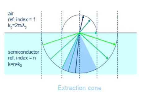
GaN-based LEDs possess has a lot of advantages for their devices, such as wide bandgap, high brightness, low power consumption, environmental stability and protection. However, there are still some problem hindered solid state lighting into reality, for example, a matter of poor light extraction for conventional board area LEDs and the poor collimation. In the Fig.1-1, refractive index of air =1 ,refractive index of GaN=2.45,
int
sec /
sec /
ext extraction
number of photons emitted into free space per ond P h number of electron injected into LED per ond I e
ν
according to Snell’s law by the following equation:
sin
sin
(
90 ,
1)
GaN c t t t t air
n
θ
=
n
θθ θ
=
n
θ=
n
=
The calculated critical angle θc is about 23° result in that the light out coupling efficiency
form the GaN surface is approximately only 4 %. The most of light will be guided in the GaN thin film layer. There are several methods have been proposed such as patterned sapphire substrates [6,7], roughening of the LED surface [8], LED surface patterning [9,10], shaping of the LED [11], and highly reflective omni-directional reflectors (ODRs) [12], to reach the high light extraction.
The other important problem is threading dislocation in GaN-based LED. Conventional GaN-based LEDs are grown on top of sapphire substrates with a low temperature GaN or AlN nuclear layer. Although the introduction of low temperature GaN or AlN nuclear layer could significantly improve the crystal quality of the subsequent GaN epitaxial layer, threading dislocation density in the order of 109~1012 cm2 will still remain in the sample due to the large difference in lattice constant and thermal expansion coefficient between sapphire and GaN.
To achieve this, the use of substrates with a low dislocation density such as GaN substrates or the epitaxial lateral overgrowth (ELOG) technique, which decrease the dislocation density of epitaxial layers is effective. By using the patterned sapphire
substrates, Tadatomo et al. [13] have successfully fabricated high output power nitride-based UV LEDs with large external quantum efficiency. Yasan et al. demonstrated 340 nm AlGaN LEDs on a hydride-vapor-phase-epitaxy -grown GaN substrate, and the device showed an output power one order of magnitude higher than similar LEDs grown on sapphire [14].
Conventional c-plane quantum-well structures suffer from the undesirable quantum-confined Stark effect (QCSE), due to the existence of strong piezoelectric and spontaneous polarizations. The strong built-in electric fields along the c-direction cause spatial separation of electron and holes that in turn gives rise to lower carries recombination efficiency, reduced oscillator strength, and blue-shifted emission.
1-4.1 Advantages of patterned sapphire substrate LEDs
However, owing to the large mismatch (~14%) of lattice constant [15] and thermal expansion (~25%) between epitaxial GaN films and sapphire substrates[16], high density dislocations ranging from 108~1010 cm-2 degrade the light-emitting diode (LED) performance profoundly. Thus, growth of GaN with low-density dislocations has been a major effort for fabrication of reliable high-efficiency LEDs. By epitaxial lateral overgrowth (ELOG) with SiNx or SiO2 mask patterned on as-grown GaN seed crystal,
technique can dramatically improve crystalline quality, the requirement of two-step growth procedure is time-consuming and easily introduced contaminations.
In recent years, the single growth technique by introducing patterned sapphire substrates (PSS) has been extensively researched. The simplified growth method can reduce the threading dislocations and increase the light extraction. The geometrical shape of the sapphire patterns can effectively scatter or redirect the guided light inside an LED chip to find escape cones, such as the hemispherical shape made by the dry etching technique [17] and the inclined c-plane facet of sapphire made by the wet etching technique [18]. In brief, the patterned sapphire substrate has some benefits:
(1) Reduced the threading dislocation
(2) Single growth process without any interruption (3) Increases the emitting light extraction efficiency
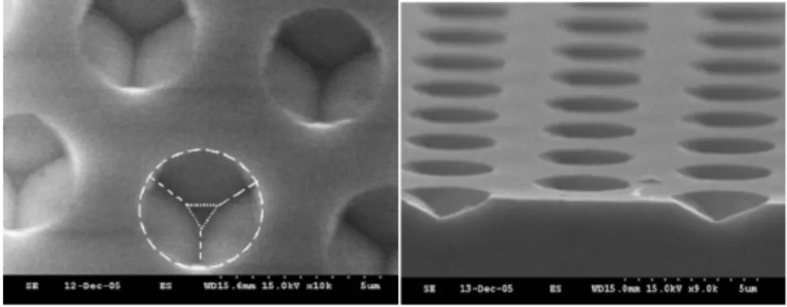
Fig.1-2 displays the schematic illustration of increased light extraction efficiency. Another technique is chemical wet etching which is a promising technique for preparing PSS show in Fig.1-3, without the need for expensive inductively coupled plasma (ICP) used in dry etching. The characteristic inclined crystallographic facets resulting from wet etching can facilitate superior light extraction efficiency. Wet-etching causes less damage
to the substrate than dry etching does, hence the sapphire surface damage induced by dry etching can be eliminated. In this study, we prepared two samples grown on conventional and patterned sapphire substrates. Cross sectional of SEM micrographs of the patterned sapphire substrate is shown in Fig.1-4. The lens height and diameter of the patterned sapphire are 1.4μm and 3.5μm, respectively. The distance between each lens is 1.0μm. We can observe the lens pattern is uniformly arranged and homogeneous size distribution. In the normal wedge shape pattern, one could reduce the threading dislocation whereas the optical emission is not enhanced appreciably. On the other hand, by using lens shaped PSS, TD density can be reduced and also optical emission efficiency could be improved due to internal reflection in the lens
1-4.2 Comparision of Sapphire substrate and GaN substrate
The semiconductors GaN, AlN, and InN have been grown primarily on sapphire, most commonly the (0001) orientation, but also on the a- and r- planes [19]. The primary reason for the decline in interest in the zincblende substrates is the inherent difficulty in growing high quality GaN in the cubic phase. Sapphire is suitable at high temperatures (~1000℃) required for epitaxial growth using the various CVD techniques commonly employed for GaN growth. However, due to the poor electrical (Electrical resistivity=10
11
-10
16
the device process steps are relatively complicated compared with other compound semiconductor devices. For devices processed on sapphire substrates, all contacts must be made from the topside. This configuration complicates contact and packaging schemes, resulting in a spreading-resistance penalty and increased operating voltages [20]. The heat dissipation of sapphire substrate was poor, therefore the commercial available GaN blue LEDs was typically operated under low current operation conditions. Therefore, GaN optoelectronics devices fabricated on electrically and thermally conducting substrate by separating sapphire substrate are most desirable. The separation of hydride vapor phase epitaxy (HVPE) grown 2-inch GaN wafer from the sapphire substrate was first demonstrated [21] by using the laser lift-off technique. The pulsed, high power UV laser of third harmonic of Q-switched Nd:YAG laser with 355 nm wavelength was used to irradiate through the transparent sapphire substrate to lift off the GaN film. The physical process responsible for the lift-off was considered by rapid thermal decomposition of GaN near the sapphire interface. For the LED grown on GaN substrate, the performance of high light output power and high current continuous wave operation condition was reported [22]. The impacts of the GaN substrates on the GaN-based LED performance are
(1) Low defect density and smooth morphology homoepitaxy (2) Good thermal conductivity and lower operation temperature
Fig. 1-1 The air/GaN interface and the totally internal reflect.
Fig. 1-3 Top and cross-sectional view SEM images of a PSS by wet etching
Chapter 2
Experiment instruments and methods
2-1 Scanning Electron Microsope-Cathodoluminescence (SEM-CL)
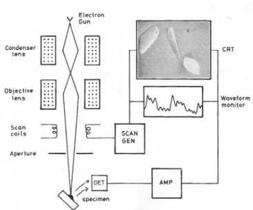
The electron microscope uses electromagnetic lenses to focus the beam to produce an image. However, SEM and TEM differ in the way images are produced and magnified. SEM is used to view the surface or near surface of a sample, whereas TEM provides information of the internal structure of thin specimens. The scanning electron microscope as the name suggests scans across the specimen by the scan coils.
As the sample is scanned by the electron beam as shown in Fig.2-1, it emits electrons and electromagnetic radiation. A detector counts the low energy secondary electrons (< 50 eV) or other radiation emitted. The image is produced by two dimensional intensity distributions by scanning a cathode ray tube (CRT) spot onto a screen and modulating the brightness by the amplified current from the detector. Three dimensional samples change the way electrons are emitted and results in the appearance of a three dimensional image. Resolutions less than 1 nm may be achieved.
2-2 Transmission electron microscope (TEM)
TEM is a method of imaging where a beam of electrons are directed through a sample after which they are scattered into discrete diffracted beams. The diffracted
electron beams are then focused in the back focal plane of the objective lens. TEM may have two modes. When operated in diffraction mode, the diffraction lens is focused on the back focal plane to produce a diffraction pattern. For the imaging mode, the diffraction lens is focused on the first image plane to produce a magnified image. In addition, the beam may be allowed to pass through the sample to obtain a bright-field image however the diffracted beams produce a dark-field image.
The ray diagram (Fig.2-2) shows (a) imaging projecting a diffraction pattern and (b) projection of an image onto a viewing screen. The interaction of the electron beam with crystalline material tends to be by diffraction. The orientation of the planes of atoms in the crystal to the electron beam changes the intensity of diffraction. TEM equipment often uses a goniometer to allow the sample to be tilted to a range of angles to obtain specific diffraction conditions. Diffracted electrons are also selected using different apertures. The intensity of diffraction is a maximum at the Bragg angle, although a variation of diffraction intensity occurs with deviation from the Bragg angle. This also depends on the thickness of the specimen. The thinner the crystal sample, the further the crystal may deviate from the Bragg condition.
When crystal planes are almost parallel to the electron beam they are close to fulfilling Bragg’s Law. The majority of electrons are diffracted when the electron beam
strikes one set of lattice planes exactly at their Bragg angle and only a few will pass through the sample undeviated. If the planes are exactly at the Bragg condition, strong diffraction will occur and the bright field image will appear dark. This variation with diffraction is shown with bend contours which are a feature of bending of the crystal planes. Dark contour images correspond to regions at the Bragg angle, while light contours result in the regions not strongly diffracting.
2-3 X-Ray Diffraction (XRD)
X-rays are a form of electromagnetic radiation with a wavelength range from 10 to 0.01 nanometers. The wavelength must be smaller that the atomic spacing of the material being analyzed. The x-rays are created from an electron beam striking a target. The beam should be monochromatic with a very small divergence obtained by collimation.
X-rays scatter from atoms by different degrees which are dependent on the atom type. However for a good quality x-ray beam incident on a well ordered crystalline material (such as a single crystal semiconductor) the scattered x-rays interfere with each other and result in a diffracted beam leaving the material. This type of diffraction is caused by parallel planes of atoms, in the same way that light may be diffracted by a diffraction grating. For any given values of x-ray wavelength and angle of incidence of the x-ray beam only one set of parallel planes will cause diffraction. This is formalized in
Bragg’s Law which states:
2 sin
n
λ
=
d
θ
Where n is an integer value, 1, 2, 3 etc., λ is the wavelength of the x-ray beam, ‘d’ is the lattice constant, the spacing between adjacent parallel planes and ‘θ’ is the angle to the normal of the plane at which the x-ray beam is incident. The diffracted beam leaves the crystal plane at the same angle from the plane’s normal as the incident beam, but in the opposite direction, as can be seen in the Fig.2-3. It shows a ‘symmetric reflection’, so called because the diffracting plane is parallel to the surface of the crystal. This is the case for diffraction from the 004 plane of a standard orientation (surface is the 001 plane) semiconductor wafer.
Figure 2-4 shows an ‘asymmetric reflection’, in which the diffracting plane is not parallel to the surface of the crystal. If the same x-ray source and beam conditioner are used then it can be safely assumed that ‘λ’ does not change. Each family of planes within a crystal has a characteristic and unique‘d’ value. It is not possible for diffraction to occur from more than one plane if a single good quality (low divergence and approximately monochromatic) x-ray beam is used. Because of this, knowing the orientation of a wafer allows any plane to be chosen as the diffracting plane.
small angle as observed in Fig.2-5, the diffracted intensity should sharply increase from zero and then sharply decrease to zero, as the x-ray beam–crystal angle passes through the Bragg angle,‘θ’. This is commonly displayed on a ‘rocking curve’, which plots the angle at which the crystal is tilted against the intensity of x-rays from the crystal.
Bragg’s Law above suggests that for a perfect single crystal and a good quality x-ray beam, one sharp peak should be seen only. Even with a perfect beam of x-rays, rocking curves for more complicated structures, such as the multiple quantum well laser will show multiple peaks.
2-4 Raman spectroscopy
Raman spectroscopy is a spectroscopic technique used to study vibrational, rotational, and other low-frequency modes in a system. It relies on inelastic scattering, or Raman scattering, of monochromatic light, usually from a laser in the visible, near infrared, or near ultraviolet range. The laser light interacts with phonons or other excitations in the system, resulting in the energy of the laser photons being shifted up or down. The shift in energy gives information about the phonon modes in the system. Infrared spectroscopy yields similar, but complementary, information.
the surface of the GaN epilayer, three Raman active phonon peaks can be clearly observed, including the E1(TO), the E2(high) and the A1(LO). Let us recall that GaN
crystallizes in a hexagonal wurtzite structure with four atoms in the unit cell and belongs to the space group. Two A1, two E1, two E2 and two B1 modes are predicted by the group
theory. One A1 and one E1 are acoustic vibrations. The E2 modes are Raman active, the
A1 and the E1 modes are both Raman and infrared active, and the B1 modes are silent.
The six Raman active phonons—i.e., A1(TO), A1(LO), E1(TO), E1(LO), E2(low) and
E2(high)— can be observed forfirst-order Raman scattering, as shown in fig. 2-7. The
E2(high) mode corresponds to the atomic oscillation in the c plane, and its mode
frequency is therefore sensitive to the lattice strain in the c plane. When the biaxial compressive stress decreases, its phonon frequency also decreases.
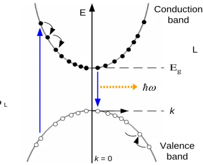
2-5 Photoluminescence spectroscopy (PL)
Photoluminescence characterization equipment generally uses the PL method to obtain the wavelength and intensity of the semiconductor material being analyzed. PL is the process of optical absorption of electrons in solids between an initial energy state Ei
and a final energy state Ef. Excitation of an electron to Ef will leave Ei unoccupied
creating a hole. Absorption creates electron-hole pairs while luminescence is the process which occurs when electrons in excited states drop to a lower level emitting a photon ħw
as shown in Fig.2-8. The electron–hole recombination creates a photon which is also known as a radiative transition. Direct gap materials are good light emitters and their optical properties are analyzed using this technique.
Photons are absorbed using an excitation source which is typically a laser. The frequency of the source ħwL must be greater than the energy gap Eg. The result is that
electrons are injected into the conduction band and holes into the valence band.
Electrons and holes are initially created in higher states within these bands but will rapidly relax to the bottom of their respective bands reaching their lowest energy state. Relaxation occurs by emitting phonons, for energy loses from the higher states, which obeys the conservation laws. The difference in energy between the two bands is Eg
which is the energy gap, also known as the band gap. Luminescence occurs close to the band gap Eg, near k = 0. After excitation, both electrons and holes relax to their lowest
energy states by emitting phonons
2-6 Electroluminescence spectroscopy (EL)
As shown in Fig.2-9, Electroluminescence (EL) is an optical phenomenon and electrical phenomenon in which a material emits light in response to an electric current passed through it, or to a strong electric field. This is distinct from light emission resulting from heat (incandescence), chemical reaction (chemiluminescence), sound
(sonoluminescence), or other mechanical action (mechanoluminescence).
Electroluminescence is the result of radiative recombination of electrons and holes in a material (usually a semiconductor). The excited electrons release their energy as photons - light. Prior to recombination, electrons and holes are separated either as a result of doping of the material to form a p-n junction (in semiconductor electroluminescent devices such as LEDs), or through excitation by impact of high-energy electrons accelerated by a strong electric field (as with the phosphors in electroluminescent displays).
Fig. 2-1 Schematic diagram of a scanning electron microscope
θ
θ
Lattice planes with spacing d X-rays with wavelengthλ
Crystal surfaceFig.2-3 Bragg diffraction from a symmetric plane
θ θ Planes not parallel with crystal surface Crystal surface
Fig.2-4 Bragg diffraction from an asymmetric plane.
2Φ
Φ
X-ray beam passing through collimator
Sample rotated or “rocked”
Scanned by detector
Fig.2-5 Geometry for x-ray rocking curve. The angle movement for the detector is twice that of the sample.
Fig.2-6 Surface Raman scattering spectrum measured from the GaN epilayer at room temperature.
k k = 0 Valence band Conduction band
ħ
ω
Egħ
ω
L E LFig. 2-8 Interband transitions in photoluminescence system
Fig.2-9 Spectrum of a blue/green electroluminescent light source for a clock radio. Peak wavelength is at 492 nm and the FWHM spectral bandwidth is quite wide at about 85 nm.
Chapter3
InGaN/GaN LEDs grown on sapphire substrate with SiO2
nanorod-array (NRA)
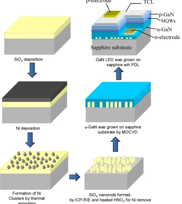
We adopted the nanorod fabrication method to fabrication SiO2 NRA on the surface
of sapphire substrate. Then we regrowth LED epi-structure on sapphire with SiO2 NRA
by nanoscale epitaxial lateral overgrowth (ELOG) method. It is not only benefit to improve the crystal quality and enhance the IQE but also advantages extraction efficiency by scattering the backside emission light upward. The schematic illustrations of GaN LED grown on sapphire with SiO2 NRA process flow chart was shown in the fig.3-1. The
preparation of the sapphire with different depth SiO2 NRA started with the deposition of
100nm, 200nm and 300nm SiO2 on the sapphire by plasma-enhanced chemical vapor
deposition (PECVD), respectively. Then, 10nm-thick Ni layer was deposited by an e-gun evaporator. The sample was annealed at 850℃ for 60s in nitrogen ambient to form self-assembled Ni nano-cluster on the SiO2 layer. The Ni nano-clusters acted as etching
masks and subsequently, the-reactive ion etching and inductive couple plasma dry etching were performed to form SiO2 NRA. After etching, the SiO2 NRA was dipped into hot
HNO3 to remove Ni cluster. The growth of a conventional GaN LED structure, which
deposited by MOCVD. A indium-tin-oxide (ITO) layer was deposited on the surface on the purpose of ohmic contact and current spreading. Lastly, the completely epitaxial structure underwent a standard four-mask LED fabrication process with a chip size 300μm×300μm. The different depth of the SiO2 NRA on the surface of sapphire were
fabrication by different SiO2 thickness and RIE time, and could be used to effectively
scatter or redirect the guiding light inside the GaN LED to escape. Moreover the epitaxial crystal quality was improved.
3-1 Process of depth dependent SiO2 NRA on sapphire substrate
3-1.1 Nano-scale Ni mask
A thin metal film can be self-assemble into nano-scale clusters after rapid thermal annealing (RTA), and the metal clusters can result in better distribution uniformity with a dielectric film deposited underneath the metal layer. A SiO2 layer was deposited on the
sapphire substrate by PECVD, followed by a thin Ni film deposition by e-gun evaporator. The RTA process to form the self-assembly nano-scale Ni clusters. The Ni nano-clusters acted as etching masks and subsequently, the-reactive ion etching and inductive couple plasma dry etching were performed to form SiO2 NRA.
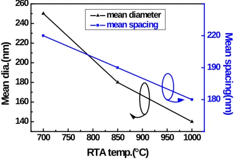
Regarding to the geometry of the Ni nano-scaled clusters, the RTA temperature and Ni thickness are important factor to determine that. In the case, we fixed the thickness of
Ni flim and vary RTA temperature from 750℃ to 1000℃ for 60s, and the results were shown in the fig. 3-2. As the RTA temperature increased from 750℃ to 1000℃, the mean diameter of Ni clusters decreased steadily from 250nm to 140nm and the spacing of Ni clusters decreased from 220nm to 180nm
In order to find out the effect of different Ni thickness, we varied the deposited Ni thickness from 50Å to 200Å on the surface of 100nm SiO2 NRA on sapphire. The RTA
temperature was at 850℃ for 60s. As the Ni thickness increasing from 50Å to 200Å, the mean diameter of Ni clusters was 35nm, 130nm, 160nm, 220nm respectively and the spacing of Ni clusters increased from was 30nm, 140nm, 170nm, 120nm respectively. The results were shown in the fig. 3-3.
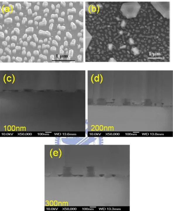
3-1.2 Fabricaiton of SiO2 NRA on sapphire
Fig. 3-4(a) shows image indicating that the SiO2 nanorods were approximately
180nm~200nm in diameter. The spacing between nanorods was about 130nm~150nm. Fig. 3-4(a) also shows that the exposed sapphire surface was flat enough for epitaxy. As the deposition process began, localized and hexagonal islandlike GaN nuclei were first form the sapphire surface to initiate GaN overgrowth, as shown in fig. 3-4(b). Fig. 3-4 (c)(d)(e) shows the cross-section SEM image of GaN epitaxial layer, where air voids were observed between the SiO2 nanorods. The existing of the voids between nanorods
observed from the micrographs suggested that not all the exposed surface enjoyed the same growth rate. Hence, only the regions with the higher growth rates, which might be originate from larger exposed surface, could play the role of a seed layer, facilitating the lateral coalescence of GaN.
3-2 InGaN/GaN LEDs grown on sapphire substrate with SiO2 NRA
3-2.1 Epitaxial characteristics of GaN film grown on sapphire substrate with SiO2
NRA
The TEM was employed to investigate the crystalline quality of GaN layers grown on a planar sapphire substrate and on sapphire with SiO2 NRA. As show in fig. 3-5(a), the
threading dislocation density (TDD) of GaN on a planar sapphire substrate was higher than 1010cm-2 due to both the large lattice mismatch (14%) and the high thermal coefficient incompatibility between sapphire and GaN. On the other hand, the crystalline quality of GaN epilayer on sapphire with SiO2 NRA was improved from that grown on a
planar sapphire substrate, as shown in fig. 3-5(b). We found that a number of stacking faults often occurred above the voids between SiO2 nanorods, where visible threading
dislocations (TDs) were rarely observed in the vicinities. It is believed that the presence of stacking faults could block the propagation of TDs. Moreover, the TDs of the GaN grown on sapphire with SiO2 NRA mainly originated from exposed sapphire surface,
which could be bent due to lateral growth of GaN. The inset of figure 3-5(b) shows the TEM image of the dislocation bending with visible turning points which also contributes to the reduction of threading dislocation.
As shown in fig.3-6, the TDs originated from the sapphire surface during the initial formation GaN growth seeds on sapphire with SiO2 NRA. The presence of voids
confirmed the lateral coalescence of GaN, leading to the bending of dislocations near the edge of SiO2 nanorods. The bent TD eventually developed into stacking faults [23] , as
depicted by Type 1 in fig. 3-6(b). Moreover, the coalescence fronts of GaN seeds provided a strain release layer where stacking faults could occur. These stacking faults were found mostly above the voids or the small GaN seeds [24], blocking the TD propagation, denoted as Type 2. Occasionally, the blocked dislocation might also be bent to form stacking faults [25]. If the growth rate was too slow to be a GaN seed, the dislocation could be blocked by the formation of voids, as illustrated by Type 3. It is also worth noting that the density of voids at the surface between sapphire and GaN was higher than that of a microscale PSS. Therefore, we believe that the formation of stacking faults and voids were involved in the reduction and bending of dislocations.
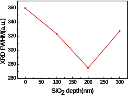
The fig. 3-7 shows XRD full-width at half- maximums (FWHMs) of the GaN films grown on flat sapphire and sapphire with 100nm, 200nm, 300nm SiO2 NRA. The
FWHMs of the ω scan rocking curve for (102) planes infer the densities of edge dislocations [26]. The FWHMs of (102) planes were 360, 323, 275 and 327 arcsec for GaN films grown on flat sapphire and sapphire with 100nm, 200nm, 300nm SiO2 NRA, respectively. The room temperature photoluminescence spectrum was also used to analyze GaN crystal quality. The peak intensity of GaN divided by peak intensity of yellow band (GaN peak/yellow peak), as shown in the fig. 3-8. The intensity of yellow band is related to defect density. The ratios of the GaN films grown on flat sapphire and sapphire with 100nm, 200nm, 300nm SiO2 NRA were 85, 91, 183 and 113, respectively. The significant decreases in XRD FWHM and increases in GaN peak/yellow peak indicate a reduction in threading dislocation density. The improvement in crystal quality is attributed to the strain relaxation of the partially relieved GaN layer in combination with the subsequent regrowth. When the initial GaN epitaxial layer was grown on sapphire, a compressive strain was built up inside the material due the mismatched lattice constants and thermal expansion coefficients between GaN and sapphire. These mismatched factors introduced threading dislocations. The NELO process relaxed the compressive strain. It acted as a buffer layer to partially filter out the problems of mismatched lattice constant and thermal expansion coefficient for MOCVD growth and resulted in improved crystalline quality.
3-2.2 InGaN/GaN multiple quantum wells grown on sapphire substrate with SiO2
NRA
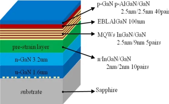
In the fig.3-9, the LED device structure was composed of 3.2μm n-GaN, 10 pairs of n-In0.08Ga0.92N/GaN(2nm/2nm) pre-strain layer, 5 pairs of In0.18Ga082N/GaN (2.5nm/9nm)
quantum wells, p-In0.16Ga084N(100nm) electron blocking layer, 40 pairs of p-AlGaN/GaN
(2.5nm/2.5nm) cap layer, Ni/Au(3nm/7nm) and Cr/Au(100nm/250nm) were subsequently evaporated onto the sample surface to serve as transparent conductive layer and p-type electrode, respectively. Ti/Al/Ni/Au contact was deposited onto the exposed n-GaN layer to serve as the n-type electrode. Finally, the epitaxial wafers were lapped down and then scribed to the fabrication of 300×300 μm2 LEDs.
3-3 Measurement and discussion
3-3.1 Photoluminesence measurement
For this study, we used the IQE method which S. Watanabe et al. proposed to determine the IQE of InGaN/GaN MQW UV LEDs. The internal quantum efficiency can be calculated by EX EX PL PL PL
E
I
E
I
C
/
/
=
η
PL photon energy and excitation photon energy, respectively. C is a constant affected by mostly carrier injection efficiency by laser, light extraction and correction efficiency of PL, and does not depend on either excitation power density or measurement temperature. First, we measured the excitation power dependent PL intensity at low and room temperature, and then the relative PL quantum efficiency curves can be obtained by using equation. And the constant C would be canceled out by normalizing the curves to the peak value at the lowest temperature, because it is independent on temperature or excitation power. From this normalization, the PL efficiency curves will not depend on carrier injection efficiency by laser, light extraction and correction efficiency of PL. Therefore, the PL efficiency would be find out from this model.
In tradition, the IQE is estimated by assuming that IQE is 100 % at lowtemperature regardless of excitation power density. However, IQE is strongly dependent on injected carrier density. Consequently, it is more reasonable to assume the peak of PL efficiency at lowest temperature is equal 100 %, and then the IQE curves as a function of excitation power and temperature can be understand.
Moreover, to avoid the absorption of GaN, the frequency doubled femtosecond pulse Ti: sapphire laser of 370 nm was used to excite sample, the excitation power density was changed from 0.01 to 15 mW, and calculated injection carrier density is about 2.0 × 10¹⁵
to 1.6 × 1018 cm-3 by using the equation below: objective active InGaN GaN GaN active loss R d d f d h P density
carrier *exp( )*(1 exp( )) *
* * * ) ( ν φ −α − −α =
where P is excitation power, hν is energy of incident light, φ is laser spot size, f is repetition rate of laser, dactiveis the active layer thickness, αGaN is the absorption of GaN,
αInGaN is absorption of InGaN, R is reflection of sample surface, and Lossobjective is
transmission loss of objective.
We first performed the power-dependent PL measurement at 15K and 300K and plot the efficiency curves of both LED on sapphire with SiO2 NRA and reference sample in
the fig.3-10 after normalizing to its peak at low temperature. For the GaN LED grown on planar sapphire, one could find that the IQE increases with injection carrier density to reach its maximum and decreases as the injected carrier density further increase. The tendency of two efficiency curves at 15K and 300K are quite similar. The corresponding density to efficiency ~48.7% in 300K is at injected carrier density of about 10-7cm-3. For the GaN LED grown on sapphire with SiO2 NRA, a similar dependence of the IQE
on the injected carrier density was observed. But under low injection carrier density range, the IQE at 15K is independent of injection carrier density. The of LED grown on planar sapphire, sapphire with 100nm, 200nm, 300nm SiO2 NRA were ~43.9%, ~49.9%,
~54.4%, and 48.8%, respectively, in 300K is at injected carrier density of 10-7cm-3. The IQE of LED grown on sapphire with 100nm, 200nm, 300nm SiO2 NRA were
enhancement by 13.7%, 26.9%, 11.2%, respectively, as compare to the LED grown on planar sapphire. We believe that the higher IQE for the LED grown on sapphire with SiO2
NRA is due to the better crystalline quality, attributed to the interaction between stacking faults and threading dislocation.
Next, we tried to understand the carrier density dependent PL at a low and room temperature case. The PL quantum efficiency at 15K increased slightly with increasing carrier density before carrier density is below 2.5×10⁻⁶cm-3. The initial stage with an increased IQE is belonging to the compensation of the nonradiative recombination centers. We find the LED grown on sapphire with SiO2 NRA is higher than that without
SiO2 NRA before 2.5×10⁻⁶cm-3. It could be explained as the LED grown on sapphire with
SiO2 NRA has fewer dislocations than the planar sample, so a higher and smoother IQE
curve is observed. The carrier density dependent PL efficiency was measured at room temperature. The measured efficiency curves were shown in Fig.3-10. The PL efficiency if both samples increased at the initial stage with a peak at about 7×10⁻⁶cm-3.and drops as the carrier density continuously increased. Since the device is operated at room temperature, the nonradiative recombination strongly dominated the efficiency
performance and that is the reason of LED grown on sapphire with SiO2 NRA enjoyed a
higher IQE than flat sample.
3-3.2 Electroluminesence measurement
The I-V curve characteristics were measured at room temperature, as shown in the fig.3-11. The forward voltages of GaN grown on sapphire without, with 100nm, 200nm and 300nm SiO2 NRA were 3.61V, 3.63V, 3.67V and 3.62V at 20mA, respectively. The
NELOG process has little impact on the LED electrical properties.
To examine the leakage current of GaN LED devices under reverse bias voltage, as shown in the fig.3-11. The leakage current of GaN grown on sapphire with SiO2 NRA
and that grown on planar sapphire were 40nA and 120nA at reverse bias voltage of -6V, respectively. The much smaller leakage current might indicate the better crystalline quality for GaN-based LED regrowth on sapphire with SiO2 NRA. It was corresponding
to what we expect in TEM images result and nanoscale-ELOG model.
Fig.3-12 shows the measured L-I curve for LED grown on sapphire with and without SiO2 NRA. The enhancement in light output power of LED grown on sapphire
with 100nm, 200nm and 300nm SiO2 NRA at injection current of 20mA were 49.6%,
77.6%, and 54.3% , respectively, as compare to the LED grown on sapphire without SiO2 NRA. We believe the enhancement in light output power is due to the improvement
of IQE and the enhanced extraction efficiency. The NRA-assisted NELO effectively suppress the threading dislocation density of GaN LED, which increased the IQE. Moreover the SiO2 NRA in GaN epilayers contributed to light extraction due to light
scattering at the interface of different refractive indices. Ueda et al [27]reported that the output power linearly increased with the surface coverage ratio of nanosilica spheres. Therefore, the extraction efficiency was enhanced by the SiO2 NRA.
3-3.3 2-Dimension FDTD simulation
The FDTD simulated model is shown in Fig.3-13. The LED structure is composed of a p-GaN, a multiquantum well (MQW) active layer, an n-GaN, and a sapphire substrate with different depth SiO2 NRA. In our simulation, the absorption coefficient of the GaN
was assumed to be 300 cm−1 , corresponding to a photon lifetime of 320fs [28] and the refractive indexes of GaN and sapphire at a wavelength of 465 nm were 2.42 and 1.77, respectively.[29]. The depths of random SiO2 NRA were 100nm, 200nm and 300nm. The
extracted light was measured at the detected top surfaces.
The enhancement in light output power was plotted as a function of SiO2 NRA depth
in the fig.3-14 . The enhancement in light output power of GaN LED grown on sapphire with 100nm, 200nm and 300nm were 14.9%, 19.4% and 11.9%, respectively. The result indicates that the dominant mechanism for an improved LED light extraction efficiency
Fig. 3-1 Schematic illustrations of GaN LED grown on sapphire with SiO2 NRA process
700 750 800 850 900 950 1000 140 160 180 200 220 240 260 mean diameter mean spacing
RTA temp.(
°C)
M
e
a
n di
a
.(
nm
)
180 190 220M
e
a
n s
pa
c
ing(
nm
)
Fig. 3-2 The relationship of mean diameter and spacing of the formed Ni nano-cluster versus the RTA temperature
4 8 12 16 20 0 50 100 150 200 250 mean diameter mean spacing
Ni thickness(nm)
M
ean
D
ia.
(n
m
)
0 50 100 150 200M
e
a
n
s
p
a
c
in
g
(n
m
)
Fig. 3-3 The relationship of mean diameter and spacing of the formed Ni nano-cluster versus the Ni thickness
Fig. 3-4 SEM image of (a) the fabrication SiO2 NRA (b) GaN nuclei on the sapphire
with SiO2 NRA as growth seeds (c) the GaN epilayer on the sapphire with 100nm
voids SiO2nanorods Stacking faults 0.2μm
(b)
(b)
Fig.3-5 The TEM images of the GaN/sapphire interface for the GaN epilayer grown on (a) a planar sapphire substrate and (b) on sapphire with SiO2 NRA. The inset of (b) shows
the dislocation bending phenomenon with visible turning points.
(a) (b)
Fig.3-6 The schematics of (a) the overgrowth process and the formation of dislocations, stacking faults, and voids at the initial stage of epitaxy, and (b) three potential
0 50 100 150 200 250 300 260 280 300 320 340 360
X
RD F
W
HM
(a
.u
.)
SiO2 depth(nm)
Fig. 3-7 XRD full-width at half- maximums (FWHMs) of the GaN films grown as a function of the SiO2 NRA depth
0 50 100 150 200 250 300 0 5 10 15 20 E nha nc e m e nt i n l ight out put pow e r( % ) SiO2 depth
Fig. 3-8 The peak intensity of GaN divided by peak intensity of yellow band as a function of SiO2 NRA depth
Fig. 3-9 The schematic of InGaN/GaN LED structure
1E13
1E14
1E15
1E16
1E17
1E18
0.0
0.2
0.4
0.6
0.8
1.0
IQ
E
(%
)
Carrier density(cm
-3)
Ref.@15K Ref.@300K 100nmNRA@15K 100nmNRA@300K 200nmNRA@15K 200nmNRA@300K 300nmNRA@15K 300nmNRA@300K-6 -4 -2 0 2 4 6 1E-4 1E-3 0.01 0.1 1 10 100
C
u
rr
e
n
t(
m
A
)
Voltage(V)
Flat 100nm NRA 200nm NRA 300nm NRAFig.3-11 I-V curves of GaN-based LED grown on sapphire with and without SiO2 NRA
100 200 300 400 0 1 2 3 4
L
ig
h
t
O
u
tp
u
t
P
o
w
e
r(
a
.u
.)
Current(mA)
Flat 100nm NRA 200nm NRA 300nm NRAFig.3-13 GaN-based LED structure for 2D FDTD simulation 0 50 100 150 200 250 300 0 5 10 15 20 E nha nc e m e nt i n l ight out put pow e r( % ) SiO2 depth
Chapter4
InGaN/GaN LEDs grown on free-standing GaN substrate
4-1 Process of free-standing GaN substrate
Fig.4-1 shows the proposed process of fabrication of the free-standing GaN substrate. In the beginning, we grew an undoped 1.8μm-thick GaN on a 2-in. c-plane sapphire substrate by metal-organic chemical vapor deposition (MOCVD). Then, a 500nm-thick SiO2 layer was deposited on the MOCVD grown-GaN layer by plasma-enhanced
chemical vapor deposition (PECVD), followed by a 20nm-thick Ni layer deposition by an e-gun evaporator. The sample was annealed at 850℃ for 60s in nitrogen ambient to form self-assembled Ni nano-cluster on the SiO2 layer. The Ni nano-clusters acted as etching
masks and subsequently, the-reactive ion etching and inductive couple plasma dry etching were performed to form GaN NRA. After etching, the GaN nanorod arrays were dipped into hot HNO3 to remove Ni cluster and buffered oxide etching (BOE) to remove SiO2
from the top of GaN nanorod arrays. We again deposited a 200nm-thick SiO2 layer on the GaN nanorod template by PECVD. After GaN nanorods template was coated with PMMA by spin coating, we used RIE and BOE to remove SiO2 on the top of GaN nanorods. Finally, we removed PMMA and grew FS GaN substrate on GaN nanorod-array with SiO2 sidewall passivation by HVPE system. The thermal expansion
coefficient difference between GaN and the sapphire substrate caused the GaN thick layer separating from the sapphire substrate.
4-1.1 Fabrication of GaN nanorods
Fig.4-2 show the SEM images indicated that the fabricated GaN nanorods were approximately 150nm to 450nm in diameter with a density of 4×109 cm-2 and the etched depth of the GaN nanorods were 1.8μm. Afterward, we again deposited a 200nm-thick SiO2 layer on the GaN nanorod template by PECVD and then utilized RIE to remove the
SiO2 layer in the top surface of GaN nanorods. The Fig.4-3 clearly exhibits the sidewalls
of GaN nanorods were surrounded by a thin SiO2 film with thickness of ~50nm.
4-1.2 GaN nanorods self-separated Hydride vapor-phase epitaxy(HVPE)
HVPE was used to regrow a 300μm-thick GaN layer, the main chemical reaction in HVPE system can be written as
For better coalescence and 2D growth, growth temperature from 950℃ to 1100℃ was selected. Series of growth parameter such as reactor pressure and V/III ratio were varied from 50 to 20 for better crystal quality. The pressure was from 500 mbar to 940 mbar for different growth steps. The Fig.4-4 shows SEM images of the initial stage of
GaN thick films growth on the GaN nanorods and many GaN islands were observed on the nanorods in the initial growing stage. The thickness of GaN bulk is approximately 3.3μm and the surface is quite rough.
The Fig.4-5 show that these GaN islands were only grown on the top of GaN nanorods, with increasing growth time, these islands coalescence , and flat GaN surfaces appeared. We can observe that GaN regrowth layer was suspended on the nanorod-array template because of the SiO2 sidewall passivation.
4-1.3 Epitaxial characteristics of free-standing GaN substrate
Fig4-6 shows the typical bright field cross-section TEM images of GaN substrate obtained from the nanorod-array. HVPE was used to regrow a 10μm-thick GaN layer. We found few threading dislocation density at GaN top surface.. A number of stacking faults often occurred above GaN nanorods, it is believed that the stacking faults could block the propagation of TDs. From the CL images, the threading dislocation density in the GaN substrate separated from GaN nanorod-arrays is estimately to be ~107 cm-2 in the Fig4-7.
During the HVPE cooling process, the 300μm-thick GaN substrate self-separates from the underlying host sapphire substrate as a result of the thermal expansion coefficient difference between GaN and the sapphire substrate. In order to release the thermal stress during HVPE cooling process, the GaN nanorods were broken and resulted
in the self-separation of GaN from sapphire substrate. Fig.4-8 shows the results of as-grown 300μm GaN films separated from GaN nanorod-arrays template and flat GaN template, respectively. A complete 2 in. self-separated free-standing GaN substrate grown on GaN nanorod-arrays template was demonstrated in Fig.4-8(a). In contrast, as shown in figure 4-8(b), the GaN grown on flat GaN template smashed into several pieces because the thermal stress cannot be released in the HVPE cooling process.
4-2 InGaN/GaN multiple quantum wells grown on free-standing GaN substrate
The material epitaxial growth uses low pressure metal-organic chemical vapor deposition (MOCVD). A 25nm of low temperature GaN nucleation layer followed by a 1.6μm u-GaN buffer layer were grown on sapphire substrate or free-standing GaN substrate. The LED device structure was 3.2μm n-GaN, 10 pairs of n-In0.08Ga0.92N/GaN(2nm/2nm) pre-strain layer, 5 pairs of In0.18Ga082N/GaN (2.5nm/9nm)
quantum wells, p-In0.16Ga084N(100nm) electron blocking layer, and 40 pairs of
p-AlGaN/GaN (2.5nm/2.5nm) cap layer Ni/Au(3nm/7nm) was and Cr/Au(100nm/250nm) were subsequently evaporated onto the sample surface to serve as transparent conductive layer and p-type electrode, respectively. Ti/Al/Ni/Au contact was deposited onto the exposed n-GaN layer to serve as the n-type electrode, as shown in Fig 4-9. Finally, the epitaxial wafers were scribed to the fabrication of 300×300 μm2 LEDs.
4-3 Measurement and discussion
4-3.1 Raman spectrum
In order to further identify the difference strain in the free-standing GaN substrate separated from nanorod-array template and flat GaN template grown on sapphire, we perform the measurement of Raman scattering. The E2-high phonon modes of
free-standing GaN and flat GaN template were located at 566.8 cm-1 and 569.6 cm-1, respectively, as shown in the Fig4-10. The E2-high peak for the GaN substrate separated
from the GaN nanorod-array template was very close to that of the strain-free GaN substrate, which is believed to be 567.1 ±0.1 cm-1.[30] Therefore, the residual stress in the GaN substrate obtained from the nanorod-array template was negligible. The residual stress could be calculated by the following equation:
where ωγand ω0 represent the Raman peaks of GaN template grown on sapphire and GaN
substrate separated from GaN nanorod-array template. The estimated value of stress is about 1.02GPa by adopting a theoretical Kγ value of 2.56cm-1/GPa report by Wanger and Bechstedt [31].
4-3.2 Electroluminesence measurement
The comparison of L-I characteristic between LED grown on FS GaN substrate and
xx r