國 立 交 通 大 學
電子工程學系 電子研究所
碩士論文
錳矽氧化物奈米點在非揮發性記憶體
應用之研究
Study on the Application of Mn-Si-O
Nanocrystal for Nonvolatile Memory
研 究 生:鄧貴宇
指導教授:張俊彥 院士
錳矽氧化物奈米點在非揮發性記憶體
應用之研究
Study on the Application of Mn-Si-O Nanocrystal
for Nonvolatile Memory
研 究 生:鄧貴宇 Student:Gui-Yu Deng
指導教授:張俊彥 院士 Advisor:Dr. Chun-Yen Chang
國 立 交 通 大 學
電子工程學系 電子研究所
碩 士 論 文
A Thesis
Submitted to Department of Electronics Engineering and
Institute of Electronics
College of Electrical and Computer Engineering
Nation Chiao Tung University
In Partial Fulfillment of Requirements
For the Degree of
Master
in
Electronics Engineering
June 2008
Hsinchu, Taiwan, Republic of China
I
錳矽氧化物奈米點在非揮發性記憶體
應用之研究
研究生: 鄧貴宇 指導教授 : 張俊彥 院士
國立交通大學
電子工程學系 電子研究所
摘要
非揮發性記憶體(NVM)目前在元件尺寸持續微縮下的需求為高密度記憶單 元、低功率損耗、快速讀寫操作、以及良好的可靠度(Reliability)。傳統浮動閘極 (floating gate)記憶體在操作過程中如果穿隧氧化層產生漏電路徑會造成所有儲 存電荷流失回到矽基板,所以在資料保存時間(Retention)和耐操度(Endurance)的 考量下,很難去微縮穿隧氧化層的厚度。非揮發性奈米點記憶體被提出希望可取 代傳統浮動閘極記憶體,由於奈米點可視為電荷儲存層中彼此分離的儲存點,可 以有效改善小尺寸記憶體元件多次操作下的資料儲存能力。 在本論文中,我們用一個簡單的製程方法來形成錳矽氧化物(MnSiOx)奈米點, 並 應 用 於 非 揮 發 性 記 憶 體 。 室 溫 下 , 在 氬 氣(Ar) 的環境中濺鍍(sputtering) Mn0.2Si0.8 薄膜,後續在氧氣環境中快速熱退火使得錳矽氧化物奈米點聚積。我 們研究發現此製程方法可形成均勻且高密度的奈米點。進一步利用 X 光光電能 譜(XPS)鑑別錳矽氧化物奈米點組成以及能隙與能帶圖建立。並藉由電流密度與 溫度關係萃取錳矽氧化物的缺陷深度。最後我們製作雙層錳矽化物奈米點記憶體 結構並探討其特性,並得到比單層奈米點較好的電荷儲存能力和保存能力。II
Study on the Application of Mn-Si-O
Nanocrystal for Nonvolatile Memory
Student: Gui-Yu, Deng Advisor: Dr. Chun-Yen, Chang
Department of Electronic Engineering and Institute of Electronics
National Chiao Tung University
Abstract
Current requirements of nonvolatile memory (NVM) are the high density cells, low-power consumption, high-speed operation and good reliability for the scaling down devices. However, all of the charges stored in the floating gate will leak into the substrate if the tunnel oxide has a leakage path in the conventional NVM during endurance test. Therefore, the tunnel oxide thickness is difficult to scale down in terms of charge retention and endurance characteristics. The nonvolatile nanocrystal memories are one of promising candidates to substitute for conventional floating gate memory, because the discrete storage nodes as the charge storage media have been effectively improve data retention under endurance test for the scaling down device.
In this thesis, an ease and low temperature fabrication technique of MnSiOx
nanocrystals was demonstrated for the application of nonvolatile memory. The
nonvolatile memory structure was fabricated by sputtering Mn0.2Si0.8 in an Ar
environment at room temperature, and then RTO process was performed to cause the
self-assembly of MnSiOx nanocrystal in the charge trapping layer. In addition, the
uniform and high density (~1012cm-2) nanocrystal can be fabricated simply in our
III
VBO and CBO between the MnSiOx films and Si substrates are also obtained by XPS
measurements. The analysis of the temperature dependence of the current density in
MnSiOx gate stacks is allowed to estimate the energy levels responsible for the
leakage current in these layers.
We also proposed a formation of Mn-Si-O nanocrystals by sputtering Mn0.2Si0.8
in the Ar/O2 environment at room temperature, and then RTA process in the N2
ambiance was performed to cause the self-assembly of MnSiOx nanocrystal in the
charge trapping layer. Sputter in O2 ambiance can avoid over oxidation and
degradation by conventional RTO process. A superior memory characteristic in term of retention characteristic is found. It’s considered that less oxygen concentration cause deeper trap level and much trap density due to oxygen vacancy.
Multi-layer MnSiOx nanocrystal memory structure is also fabricated and
discussed. Multi-layer nanocrystals have better charge storage and retention over single-layer nanocrystals.
IV
誌 謝
隨著本篇論文的完成,代表著學生生涯的結束,不需要再準備期中期末考, 但也意味著人生下一階段的開始;這兩年碩士生活受過太多人的幫忙,往日的回 憶歷歷在目,在此由衷的感激你們。帶著複雜的心情,我畢業了! 首先要特別感謝我的指導教授張俊彥院士,非常高興能夠進入這個實驗室。 感受了老師對實驗的熱誠與執著,以及在學術上宏觀的看法,開拓了我的思維與 氣度。張鼎張教授在實驗上提供完善的資源、設備;遇到瓶頸時亦能給予適時的 幫助與建議,使得實驗能順利完成,非常感謝老師們的指導。 在交大兩年的研究生涯裡,非常感謝和我朝夕相處的學長姐、同學、學弟們; 奈米組的峻豪(真歡樂的土撥)、大山、富明、世青、致宏、立偉(KTV 真假音莫 變)、昭正(人肉點唱機秋秋令)、緯仁(改走諧星路線威學長)、志瑋(重色輕友一號 老胡)、仕承、佳州、彥廷(對助理念念不忘小馬)、俐婷、麗雯、睿龍(過河拆橋 AP 龍)、鵬博,承恩(重色輕友二號少爺)以及 TFT 組的皓彥、泓緯、宛芳等學長 姐,謝謝你們在實驗上給我很多寶貴的意見,不管是研究上的精神以及做人做事 應有的態度,在你們身上我學習到很多。同時,也要感謝快速電子實驗室的宗熺、 心卉、怡誠、兆欽、哲榮、詩國、峻丞、弘斌學長姊們,以及實驗室助理芮頤除 了平時對我的照顧及關心之外,也從你們身上學到許多研究的精神。 我的同學們,成能(新好男人 JJ)、勝杰(門禁卡獸杰)、述穎(永遠被噹一號師 傅)、培堃(方方土)、凱庭(大頭)、元駿(狗哥)、聖錡(CP 值超高廉價勞工)、派璿、 巍方(室友巍哥)、逸立(永遠被噹二號)、威廷;以及簡博實驗室的欣哲、弘森、 敬倫有你們的陪伴,無塵室裡一起奮鬥的日子將是我一生最難忘的回憶。另外還 要感謝志文、信淵(418 稱王?)、耀峰(吱吱峰)、侑庭、誌陽(勾勾羊)等學弟們, 感謝你們在生活及實驗上的幫忙,也常給實驗室帶來歡笑氣氛。 在此特別感謝中山的崎峰、書瑋、敏甄學長姐,有你們的協助才能讓我的論 文更充實;還有成大的柯榮明大哥,謝謝您提供寶貴的人生經驗給我,也很敬佩V 您的求學精神; 以及幫忙看 TEM 清大的偉鑫學長、奈米科技中心鍾小姐,以 及眾多美美的XPS 小姐們。還要謝謝大同的小四,謝謝你們在實驗上的幫忙與 鼓勵。 最後,要感謝我親愛的爸爸鄧鴻明先生、媽媽劉阿滿女士;大學四年、碩士 兩年在外地求學的我,和家人相聚的時間變少,感謝你們的體諒,在精神與生活 上的支持與鼓勵,讓我無後顧之憂完成這個碩士學位,這六年來,辛苦你們了; 僅以此論文獻給你們。 鄧貴宇 於 交通大學 2008 年
VI
Contents
Chinese Abstract………....………...………..Ⅰ
English Abstract………..………….………..II
Acknowledgement...IV
Contents………....…...………VI
Table Captions……….…….………VIII
Figure Captions………...………...IX
Chapter 1 Introduction
1.1 Overview of Nonvolatile Memory…..…………..………...….……....……..1
1.1.1 Nanocrystal Nonvolatile Memory Devices……….…...……….……..3
1.1.2 SONOS Nonvolatile Memory Devices…………...…..……..……7
1.2 Organization of This Thesis………..………...…………10
Chapter 2 Basic Principle of Nonvolatile Memory
2.1 Introduction...132.2 Basic Program/Erase Mechanisms...14
2.2.1 Energy band diagram during program and erase operation…...14
2.2.2 Carrier injection mechanis…...……….…..…………...15
2.3 Basic Reliability of Nonvolatile Memory...20
2.3.1 Retention………..………...…..20
2.3.2 Endurance……….………...…...20
2.4 Basic Physical Characteristic of Nanocrystal NVM...21
2.4.1 Quantum Confinement Effect………..……..…...…...22
2.4.2 Coulomb Blockade Effet………..……..………...……22
Chapter 3 Formation, Energy band diagram and Nonvolatile
Memory Characteristics of Manganese Silicate Nanocrystals
VII
3.1 Motivation………...……….33
3.2 Failure analysis for fabrication of MnSiOx nanocrystals...34
3.2.1 Experimental Procedures………..….…..…….…….34
3.2.2 Results and Discussions………...………..…...34
3.3 Formation of MnSiOx nanocrystals by RTO process...35
3.3.1 Experimental Procedures……….………..….35
3.3.2 Results and Discussions………..…..36
3.4 Summary I………..…..39
Chapter 4 Formation and Nonvolatile Memory Characteristics of
MnSiO
xNanocrystals by Sputter in O
2ambiance
4.1 Formation of MnSiOx nanocrystals by sputter in O2 ambiance………..….514.1.1 Experimental Procedures………...………..…….51
4.1.2 Comparison of Electrical Characteristics between RTO and Sputter in O2 Ambiance Process……….….52
4.2 Summary II...53
Chapter 5 Multi-Layer Manganese Silicate Nanocrystals Memory
5.1 Formation of Multi-Layer MnSiOx NCs Memory………...595.1.1 Experimental Procedures………...59
5.1.2 Comparison of Electrical Characteristics between Multi-Layer and Single-Layer MnSiOx NCs Memories………...…60
5.2 Summary ...Ⅲ ...60
Chapter 6 Conclusion
6.1 Conclusions...65VIII
Table Captions
Chapter 4
Table 4-1 Comparisons of oxygen concentration for different process by ESCA analysis………...58 Table 4-2 Comparisons of memory characteristics for different process ………..58
IX
Figure Captions
Chapter 1
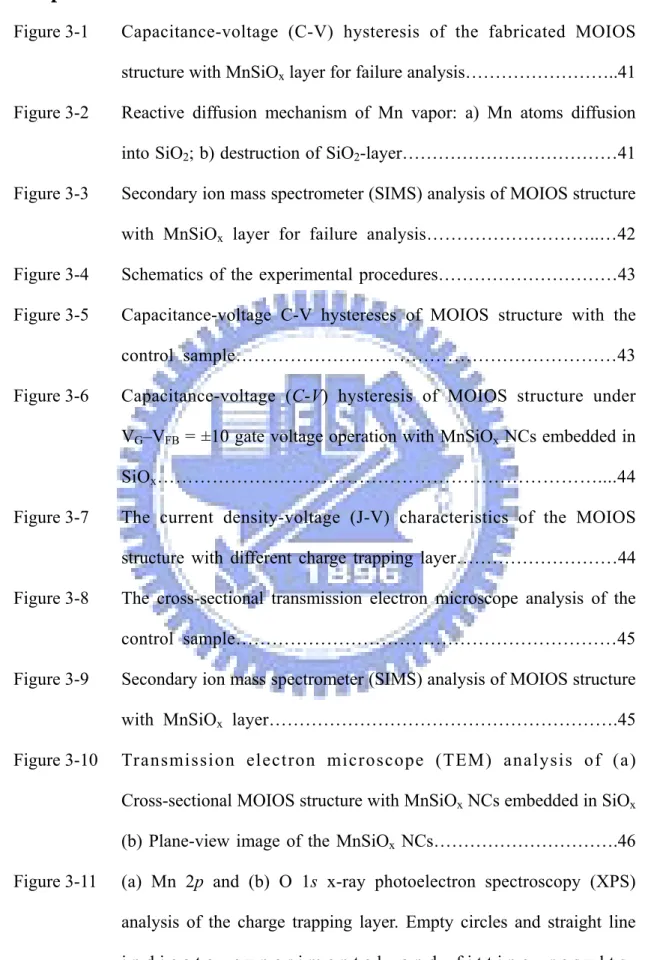
Figure 1-1 The structure of the conventional floating gate nonvolatile memory
device. Continuous poly-Si floating gate is used as the charge storage element...11
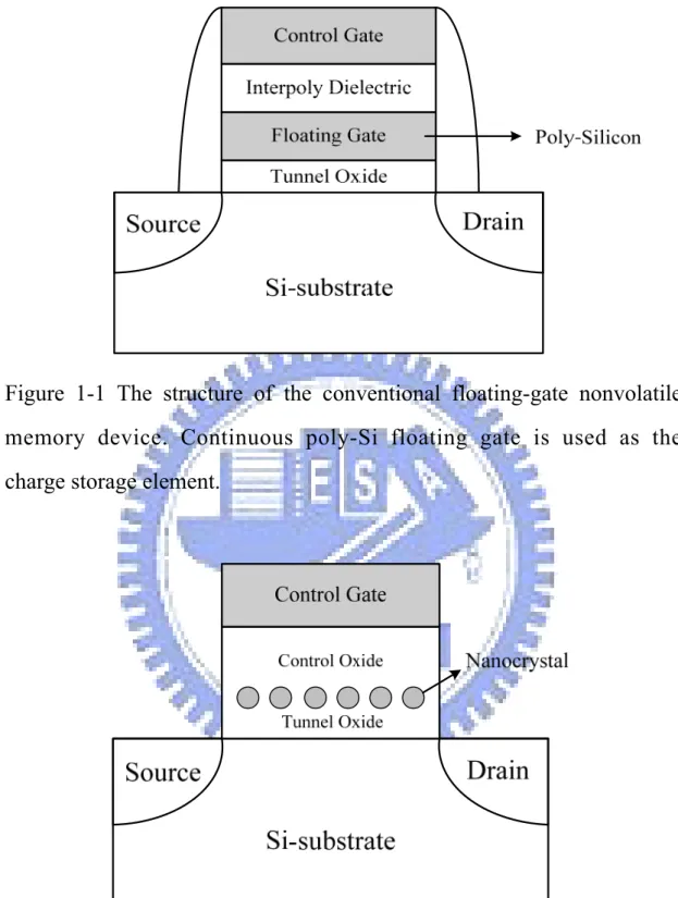
Figure 1-2 The structure of the nanocrystal nonvolatile memory device. The
semiconductor nanocrystals or metal nanocrystals are used as the charge storage element instead of the continuous poly-Si floating gate………...11
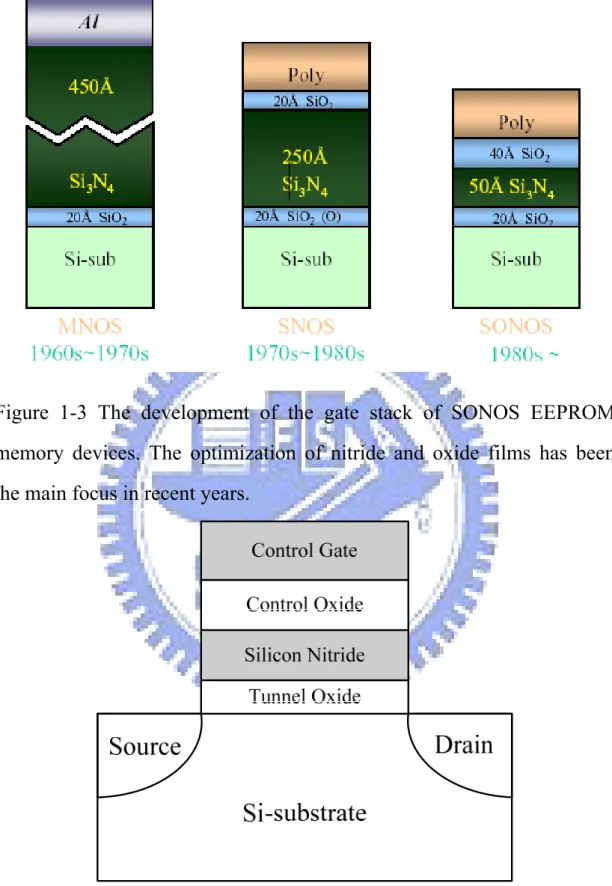
Figure 1-3 The development of the gate stack of SONOS EEPROM memory
devices. The optimization of nitride and oxide films has been the main focus in recent years………12
Figure 1-4 The structure of the SONOS nonvolatile memory device. The nitride
layer is used as the charge-trapping element………..12
Chapter 2
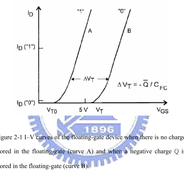
Figure 2-1 I–V curves of an FG device when there is no charge stored in the FG
(curve A) and when a negative charge Q is stored in the FG (curve B)...24
Figure 2-2 Energy band diagrams of a dual-channel SONOS transistor under (a)
program (b) erase operation.● electrons, ○ holes………..25
Figure 2-3 (a) Schematic cross-section of nanocrystal memory device structure;
(b) illustration of write process: inversion- layer electron tunnels into the nanocrystal; (c) illustration of erase process: accumulation layer
X
hole tunnels into the nanocrystal, electron in nanocrystal can tunnel back to the channel………...26
Figure 2-4 Fourth approaches to programming methods, described by Hu and
White. (a) Direct tunneling (DT) (b) Fowler-Nordheim tunneling (FN) (c) modified Fowler-Nordheim tunneling (MFN) (d) trap assistant tunneling (TAT)……….…27 Figure 2-5 Schematic cross section of MOSFET. The energy-distribution function
at point (X1,Y1) is also shown………28
Figure 2-6 A schematic energy band diagram describing the process involved in electron injection………29 Figure 2-7 Energy-band diagram for the proposed band to band induce hot electron injection mechanism and schematic illustration cross of the Flash memory with p-channel cell. Due to the positive bias to the c o n t r o l g a t e , h o l e s a r e n o t i n j e c t e d i n t o t h e t u n n e l oxid……….………..30 Figure 2-8 Band to band induce hot hole injection mechanism and schematic
illustration cross of the Flash me mory with p-channel cell………...………...31 Figure 2-9 A typical result of an endurance test on a single cell. Threshold voltage window closure as a function of program / erase cycles on a single cell...31 Figure 2-10 Anomalous SILC modeling. The leakage is caused by a cluster of
positive charge generated in the oxide during erase. The multitrap assisted tunneling is used to model SILC: trap parameters are energy and position………...32
XI
Chapter 3
Figure 3-1 Capacitance-voltage (C-V) hysteresis of the fabricated MOIOS
structure with MnSiOx layer for failure analysis………..41
Figure 3-2 Reactive diffusion mechanism of Mn vapor: a) Mn atoms diffusion
into SiO2; b) destruction of SiO2-layer………41
Figure 3-3 Secondary ion mass spectrometer (SIMS) analysis of MOIOS structure
with MnSiOx layer for failure analysis………..…42
Figure 3-4 Schematics of the experimental procedures………43
Figure 3-5 Capacitance-voltage C-V hystereses of MOIOS structure with the
control sample………43
Figure 3-6 Capacitance-voltage (C-V) hysteresis of MOIOS structure under
VG–VFB = ±10 gate voltage operation with MnSiOx NCs embedded in
SiOx………....44
Figure 3-7 The current density-voltage (J-V) characteristics of the MOIOS structure with different charge trapping layer………44
Figure 3-8 The cross-sectional transmission electron microscope analysis of the
control sample………45
Figure 3-9 Secondary ion mass spectrometer (SIMS) analysis of MOIOS structure
with MnSiOx layer……….45
Figure 3-10 Transmission electron microscope (TEM) analysis of (a)
Cross-sectional MOIOS structure with MnSiOx NCs embedded in SiOx
(b) Plane-view image of the MnSiOx NCs……….46
Figure 3-11 (a) Mn 2p and (b) O 1s x-ray photoelectron spectroscopy (XPS) analysis of the charge trapping layer. Empty circles and straight line i n d i c a t e e x p e r i m e n t a l a n d f i t t i n g r e s u l t s , respectively………..…..46
XII
Figure 3-12 Valence band spectrum for Si-sub, 5 nm thick SiO2 /Si(100) and 5 nm
thick MnSiOx /Si(100)………...47
Figure 3-13 O 1s energy-loss spectra for 5 nm thick thermal oxide and 5nm thick
MnSiOx……….…….47
Figure 3-14 Retention characteristics of the MnSiOx NCs memory structure which
using gate voltage stress until initial VFB shift = ±2V at room
temperature………48 Figure 3-15 Schematics of charge storage states…….. ………48
Figure 3-16 Endurance characteristics of the MnSiOx NCs memory………49
Figure 3-17 Current–density JG as a function of the VOX of a MOS capacitor with a
SiOx /MnSiOx stack dielectric layer (8 nm MnSiOx) recorded from 25
to 150 °C………50 Figure 3-18 Current–density JG as a function of the inverse temperature for
SiOx/MnSiOx gate dielectric stacks. The solid lines are fits to the data
using Eq.(2)………50
Chapter 4
Figure 4-1 Schematics of sputter in O2 ambiance process……….………..54
Figure 4-2 Transmission electron microscope (TEM) analysis of cross-sectional
MOIOS structure with MnSiOx NCs by sputter in O2 ambiance process.
The diameter and density of the NCs is approximately 6 nm and
2.13×1012 cm-2………..…………..54
Figure 4-3 Capacitance-voltage (C-V) hysteresis of MOIOS structure by (a)
sputter in O2, and (b) RTO process. The memory windows of two
samples are nearly equal to 1 and 2.5 V under VG-VFB=±5 dash line
XIII
respectively………....…..55
Figure 4-4 Endurance characteristics of the NC memory structure by (a) sputter in
O2, and (b) RTO process. Pulses condition of VG−VFB= ± 9V for
10ms………...55
Figure 4-5 Retention of the NC memory structure by RTO process is 35%. Charge
holding rate of the NC memory structure by sputter in O2 process is
52%...56
Figure 4-6 Current–density JG as a function of the inverse temperature for SiOx
/MnSiOx gate dielectric stacks. The solid lines are fits to the
data ………57
Figure 4-7 The trap level of MnSiOx NCs by RTO blue line and sputter in O2 blue
line process……….57
Chapter 5
Figure 5-1 Schematics of double layer MnSiOx NCs process……….62
Figure 5-2 Transmission electron microscope (TEM) analysis of cross-sectional
MOIOS structure with double-layer MnSiOx NCs. The diameter and
density of the NCs is approximately 6nm……….62
Figure 5-3 Endurance characteristics of (a) double layer and (b) single layer NCs
memory structure. Pulses condition of VG−VFB= ± 9 V for
10ms………..63
Figure 5-4 Capacitance-voltage (C-V) hysteresis of (a) double layer and (b) single
layer NCs memory structure. The memory windows of two samples
are nearly equal to 1 under VG-VFB=±5 dash line. Double layer NC
shows larger than single layer NC under VG-VFB=±10 V solid line gate
XIV
Figure 5-5 (a) Memory window characteristics of the multi-layer MnSiOx
nanocrystal memory as compared with single-layer MnSiOx
nanocrystal memory (b) A simple energy band diagram of small gate voltage (c) high gate voltage operation………64
Figure 5-6 (a) Retention characteristics of the multi-layer MnSiOx nanocrystal
memory as compared with single-layer MnSiOx nanocrystal memory
(b) A simple energy band diagram of single-layer (c) multi-layer NCs……….64
1
Chapter 1
Introduction
1.1 Overview of Nonvolatile Memory
Recently, the portable electronic products find wide applications. These products are all based on flash memory which is considered as a technology driver for semiconductor industry in the next generation. It can be classified into two major markets: code storage application and data storage application. NOR type flash memory [1.1] has been targeted at code storage application, such as PC bios and DVD player. NAND type flash memory [1.2] is most suitable for code storage application, such as PDA, memory cards, MP3 audio players, digital cameras, and USB flash personal disc etc. These products all are based on flash memory that is nonvolatile and can keep stored information when the power supply is switched off. Flash memory also has exhibited several advantages, such as the ability to be electrical programmed and fast simultaneous block electrical erased in a single-cell, smallest cell size to achieve highest chip density, and good flexibility [1.3-1.4]. The flash memory fabrication process can be compatible with the current CMOS process and be a suitable solution for embedded memory application. Flash memories are easily scale down and replacement for EPROMs (Erasable Programmable Read Only Memory) and EEPROMs (Electrically Erasable Programmable Read Only Memory). As these critical advantages flash memory possesses, it has become the mainstream nonvolatile memory device in last few decades.
In 1967, D. Kahng and S. M. Sze invented the floating-gate (FG) nonvolatile semiconductor memory (or flash memory) at Bell Labs [1.5]. A standard conventional floating-gate device structure is shown in Fig. 1-1. The structure is basic on a Metal Oxide Semiconductor Field Effect Transistor (MOSFET) with a modified stacking
2
gate which composed by control gate, dielectric, floating gate and dielectric as a sandwich structure. Charge injected in the FG is maintained there, allowing the difference between threshold voltages of the cell transistor for nonvolatile memory application.
Nowadays, nonvolatile memory devices are moving toward high density memory array, low cost, low power consumption, high-speed operation, and good reliability. Although conventional flash memory does not require refreshing and thus consumes less power and achieves much higher array density with a stacked floating gate
structure. The most prominent one is the limited potential for continued scaling of the
device structure. This scaling limitation stems from the extreme requirements put on the tunnel oxide layer. The tunnel oxide must be thin enough to allow quick and efficient charge transfer to and from the FG. But conventional FG memory devices have limited potential for aggressive scaling of the tunnel oxide thickness. The tunnel oxide needs to provide superior isolation under retention, endurance, and disturbed conditions in
order to guarantee the data integrity for 10 years. For faster operation speed, thin
tunnel oxide is desirable. However, it is desirable to increase the thickness of tunnel oxide for better isolation and reliability. So there is a trade-off between speed and reliability for the optimum tunnel oxide thickness. Currently, the tunnel oxide of the commercial flash memory devices is about 8-11nm, Resulting in high programming voltage and slow programming speed [1.6].
For the conventional FG memory, if there are several defects in the tunnel oxide after programming or erasing operated steps, might induce a leakage path. That make all charge stored in the FG leak back to the channel. To alleviate the tunnel oxide design trade-off for floating-gate memory devices, memory-cell structures employing discrete traps as charge storage media have been proposed. Unlike conventional continuous floating gate, charges stored in discrete nodes cannot easily redistribute
3
amongst themselves. Therefore, only a relatively small number of nodes near the oxide defects will be affected. Local charge storage in discrete nodes enables more aggressive scaling of the tunnel oxide by relieving the total charge loss concern.
Therefore, two suggestions, poly-Si/oxide/nitride/oxide/Si (SONOS) [1.7-1.9] and
nanocrystal nonvolatile memory devices [1.10-1.12] are proposed to overcome this
oxide quality limit of the conventional FG structure. Hence the tunnel oxide thickness can be reduced to allow faster programming and lower voltage operation.
1.1.1 Nanocrystal Nonvolatile Memory Devices
Nanocrystal nonvolatile memories are one particular implementation of storing charge by dielectric surround nanodots, and were first introduced in the early 1990s by IBM researchers who proposed flash memory with a granular floating gate made from silicon nanocrystals [1.13]. The name nanocrystal referred to a crystalline structure with a nanoscale dimension. Fig. 1-2 illustrates conventional nanocrystal nonvolatile memory (NVM) device structures. It is observed that the nanocrystals are separated from each other within the gate dielectric. Its electronic properties seem more similar to an atom or molecule rather than the bulk crystal. In the nanocrystal nonvolatile memory device, the charges were charged in the isolated nanocrystals instead of the continuous FG polysilicon layer. Each nanodots will typically store only a handful of electrons; collectively the charges stored in these dots control the channel conductivity of the memory transistor.
Nanocrystal-based NVM devices have recently received much attention due to their potential to overcome the limitations of conventional polysilicon-based flash memory. Using nanocrystals as charge storage media offers several advantages, the main one being the potential to use thinner tunnel oxide without sacrificing
4
non-volatility. This is a quite attractive proposition since reducing the tunnel oxide thickness is a key to lowering operating voltages and/or increasing operating speeds. This claim of improved scalability results from the local charge storage in discrete nodes, which makes the storage more fault-tolerant and immune to the leakage caused by localized oxide defects. Further, the lateral charge migration effect between nanocrystals can be suppressed by the strongly isolation of surrounded dielectric. There are other important advantages though. First, nanocrystal memories use a more simplified fabrication process as compared to conventional stacked-gate FG NVM’s by avoiding the fabrication complications and costs of a dual-poly process. Second, due to the absence of drain to FG coupling, nanocrystal memories suffer less from drain-induced-barrier-lowering (DIBL) and therefore have intrinsically better punch-through characteristics. One way to exploit this advantage is to use a higher drain bias during the read operation, thus improving memory access time [1.14]. Alternatively, it allows the use of shorter channel lengths and therefore smaller cell area. Finally, nanocrystal memories are characterized by excellent immunity to stress induced leakage current (SILC) and oxide defects due to the distributed nature of the charge storage in the nanocrystal layer. Research in this regime has focused on the development of fabrication processes and nanocrystal materials, and on the integration of nanocrystal-based storage layers in actual memory devices.
The fabrication of a nonvolatile memory cell requires a perfect control of four main parameters: (1) the tunnel oxide thickness, (2) the nanocrystal density, (3) the nanocrystal size, and (4) the control oxide thickness. An important consideration is the average size and aerial density of the nanocrystals. Larger-size nanocrystal array provides higher program/erase efficient due to small quantum confinement and coulomb blockade effects, and hence larger tunneling probability. However, it is desirable to reduce the nanocrystal size for better reliability (stress induced leakage
5
during retention). So there is a trade-off between programming speed and reliability in
selecting the nanocrystal size. A typical target is a density of at least 1012 cm-2, and
requires nanocrystal size of 5 nm and below. Moreover, good process control is needed with regards to such nanocrystal features as: planar nanocrystal layer; inter-crystal interaction (lateral isolation); and crystal doping (type and level). Finally, it is preferred that that the fabrication process is simple and that it uses standard semiconductor equipment.
After the first proposal of a memory transistor using silicon nanocrystals as floating gates. In order to improve the data retention in NVM, double layer Si nanocrystals memory has been investigated [1.15]. It seems interesting to use Ge nanocrystals rather than Si nanocrystals because of its smaller band gap. Indeed King and Hu have recently demonstrated the superior memory properties of Ge based nanocrystal memories over those based on Si [1.16]. Recently, germanium/silicon (Ge/Si) nanocrystals have been reported to possess superior charge retention capability than Ge or Si nanocrystals. This is due to the fact that Ge has a smaller band gap than Si and thus by introducing a Si interface around the Ge nanocrystal, it would create an additional barrier height at the Ge/Si interface which makes it harder for electrons to leak out of the nanocrystal [1.17, 1.18]. However, semiconductor nanocrystal memory may not be the ultimate solution to nonvolatile memory scaling, although it still attracts a lot of attention now.
In optimizing nanocrystal NVM devices, the ideal goal is to achieve the fast write/erase of DRAM and the long retention time of Flash memories simultaneously. For this purpose we need to create an asymmetry in charge transport through the gate
dielectric to maximize the IG, Write/Erase/ IG, Retention ratio. One approach for achieving
this goal is to engineer the depth of the potential well at the storage nodes, thus creating a small barrier for writing and a large barrier for retention between the
6
substrate and the storage nodes. This can be achieved if the storage nodes are made of metal nanocrystals by engineering the metal work function. The major advantages of metal nanocrystals over semiconductor nanocrystals include higher density of states around the Fermi level, scalability for the nanocrystal size, a wide range of available work functions, and smaller energy perturbation due to carrier confinement [1.19]. In addition, an electrostatic modeling from both analytical formulation and numerical simulation is demonstrated that the metal nanocrystals will significantly enhance the electric field between the nanocrystal and the sensing channel set up by the control gate bias, and hence can achieve much higher efficiency in low-voltage P/E [1.20].
Toward better NVM device performance and reliability, numerous attempts have been made using metal nanocrystals. Liu et al. reported the growth of Au, Pt, and Ag
nanocrystals on SiO2 using an e-beam deposition method [1.19]. Lee et al. proposed a
NVM structure using the Ni nanocrystals and high-k dielectrics [1.21]. Chen et al. present the stacked Ni silicide nanocrystal memory was fabricated by sputtering a comix target followed by a low temperature RTO process [1.22]. W nanocrystals on
atomic-layer-deposited HfAlO/Al2O3 tunnel oxide were presented for application in a
memory device [1.23]. Using W nanocrystal double layers embedded in HfAlO to enhancement of memory window was demonstrated from the short channel devices down to 100nm [1.24]. Tang et al demonstrate that a chaperonin protein lattice can be used as a template to assemble PbSe and Co nanocrystal arrays for Flash memory fabrication. This provides a new approach to achieve a high density and good distribution uniformity nanocrystal array [1.25].
In the future, the primary drivers behind nanocrystal memories are the potential to scale the tunnel oxide thickness, resulting in lower operating voltages, and the simplicity of a single poly-silicon process. But there are still challenges await nanocrystal memories in the long road to commercialization. Nanocrystal memories
7
have yet to deliver on most of their promises. In reality, part of the voltage gain is offset because of the poor control gate coupling. For fabrication processes, it is hard to control the uniformity of the nanocrystal size and their physical locations in the channel. It is not a surprise that nanocrystal memories exhibit large device-to-device variation. Moreover, it has yet to be demonstrated that both the nominal and the statistical retention behavior are sufficient to meet true non-volatility requirements. Although single-dot memories have been demonstrated [1.26,1.27], but a more fundamental understanding of the scaling limits of nanocrystal memories is necessary, concentrating especially on the aspect of controlling channel conductance when relying on only a few discrete charge centers [1.28]. Finally, in order for that to happen, their claimed benefits will need to be more unambiguously substantiated, and a more appealing bundle of memory features will have to be demonstrated.
1.1.2 SONOS Nonvolatile Memory Devices
The first nitride-base devices is metal-gate nitride device MNOS
(Metal/Nitride/Oxide/Silicon) which was reported in 1967 by Wegener et al [1.29]. However, it is well known that silicon nitride film contains much carrier traps which cause threshold voltage shift. Then the silicon nitride trap-based devices are widely studied for charge storage device application in the early 70s. Fig. 1-3 illustrates the progression of device cross section, which has led to the present SONOS device structure. Initial device structures in the early 1970s were p-channel metal-nitride-oxide-silicon (MNOS) structures with aluminum gate electrodes and thick (45nm) silicon nitride charge storage layers. Write/erase voltages were typically 25-30 V. In the late 1970s and early 1980s, scaling moved to n-channel SNOS devices with write/erase voltages of 14-18 V. In the late 1980s and early 1990s, n- and
8
p-channel SONOS devices emerged with write/erase voltages of 5-12 V. The ONO triple dielectric structure has some advantages, such as (1) lower programming voltage since the blocking action of the top oxide removes any limitation on the reduction of the nitride thickness; (2) charge injection from and to the gate electrode
is minimized for both gate polarities, particularly for hole injection; (3) improved
memory retention since there is minimal loss of charge to the gate electrode.
The SONOS (poly-Silicon-Oxide-Nitride-Oxide-Silicon) memory devices, as shown in Fig. 1-4, have attracted a lot of attention due to its advantages over the traditional floating-gate flash device. These include reduced process complexity, lower voltage operation, high speed operation, improved cycling endurance, and elimination of drain-induced turn-on [1.30-1.32]. The main difference between floating-gate and SONOS structure is the method of charge storage. Conventional FG structure charges carrier in the continuous conductive polysilicon. In contrast with conventional FG structure, SONOS structure charge carrier in the physical discrete
traps of the silicon nitride dielectric. A typical trap has a density of the order 1018-1019
cm-3 according to Yang et al [1.33] and stores both electrons and holes injected from
the channel. The charge stored in the silicon nitride cannot move easily, hence the SONOS can bear the defect in the tunnel oxide induced the leakage path. Therefore, the SONOS memory device has better endurance the conventional FG memory.
The SONOS memory devices still face challenge in the future for high density nonvolatile memory application, which requires low voltage (< 5V), low power consumption, long-term retention, and superior endurance. Various approaches have been proposed for improving the SONOS performance and reliability. Chen et al.
demonstrated a Si3N4 bandgap engineering (BE) control method for better endurance
and retention. A nitride with varied relative Si/N ratio throughout the film has increased the charge-trapping efficiency significantly [1.34].
9
In recent research, high-k dielectric materials were proposed to replace the
silicon nitride film as trapping layer, such as HfAlO and Al2O3. Tan et al. showed that
over-erase phenomenon in SONOS memory structures can be minimized by replacing
silicon nitride with HfO2 as the charge storage layer. The charge retention and
endurance performance is improved by the addition of 10% Al2O3 in HfO2 to form
HfAlO, while maintaining the over-erase resistance of HfO2 [1.35]. She et al.
demonstrates that high-quality nitride is applied as the tunnel dielectric for a
SONOS-type memory device. Compared to control devices with SiO2 tunnel
dielectric, faster programming speed and better retention time are achieved with low
programming voltage [1.36]. Lee et al. presents a device structure of SiO2/SiN/Al2O3
(SANOS) with TaN metal gate. It is demonstrated that the use of TaN metal gate
blocks electron current through Al2O3 layer more efficiently than a conventional
polysilicon gate, resulting in faster program/erase speed and significant decrease of
the saturation level of the erase VT [1.37].
Chen et al. studies a polycrystalline silicon thin-film transistor (poly-Si TFT) with oxide/nitride/oxide (ONO) stack gate dielectrics and multiple nano-wire channels for the applications of both nonvolatile silicon-oxide-nitride-oxide-silicon (SONOS) memory and switch transistor [1.38]. The proposed NW SONOS-TFT exhibits superior memory device characteristics with high program/erase efficiency and stable retention characteristics at high temperature. Such a SONOS-TFT is thereby highly promising for application in the future system-on-panel display applications.
New device structures are also indispensable in making flash memory more scalable. Since SONOS flash memory offers a thinner gate stack than floating gate flash memory, and a FinFET structure controls the short channel effect much better than a bulk structure. It has been demonstrated that the FinFET SONOS flash memory
10
devices with a much smaller cell size can provide both excellent performance and reliability. Therefore, FinFET SONOS memory has potential to become the candidate for the next generation flash memory [1.39-1.40].
1.2 Organization of This Thesis
In Chapter 1, general background of flash, SONOS, and nanocrystal nonvolatile
memory devices are introduced.
In Chapter 2, basic principle of nonvolatile memory is introduced.
In Chapter 3, formation, energy band diagram and nonvolatile memory
characteristics of manganese silicate nanocrystals.
In Chapter 4, formation and nonvolatile memory characteristics of MnSiOx
nanocrystals by sputter in O2 ambiance.
In Chapter 5, multi-layer manganese silicate nanocrystals memory.
Figure 1-1 The structure of the conventional floating-gate nonvolatile
memory device. Continuous poly-Si floating gate is used as the
charge storage element.
Figure 1-2 The structure of the nanocrystal nonvolatile memory device.
The semiconductor nanocrystals or metal nanocrystals are used as the
charge storage element instead of the continuous poly-Si floating gate.
Figure 1-3 The development of the gate stack of SONOS EEPROM
memory devices. The optimization of nitride and oxide films has been
the main focus in recent years.
Figure 1-4 The structure of the SONOS nonvolatile memory device.
The nitride layer is used as the charge trapping media.
Chapter 2
Basic Principle of Nonvolatile Memory
2.1 Introduction
There is a widespread variety of Nonvolatile Memory (NVM) devices, and they all show different characteristics according to the structure of the selected cell and the complexity of the array organization. A NVM memory cell has to commute from one state to the other and that can store the information independently of external conditions. There are several methods to achieve the NVM memory characteristic,
such as transistor VT shifts, charge displacements, and resistance change [2.1]. In this
thesis, we focus on one solution that a transistor with a threshold voltage that can change repetitively from a high to a low state, corresponding to the two states of the memory cell. Most operations with a shift in the threshold voltage on novel nonvolatile memories, such as nanocrystal and SONOS memories are base on the concept of Flash memory. If a datum has to be stored in a bit of the memory, there are different procedures. The threshold voltage shift of a Flash transistor can be written as [2.2][2.3]: FC T C Q V =− Δ 13
where Q is the charge weighted with respect to its position in the gate oxide, and the capacitances between the floating gate and control gate. The threshold voltage of the memory cell can be altered by changing the amount of charge present between the gate and the channel, corresponding to the two states of the memory cell, i.e., the binary values (“1” and “0”) of the stored bit. Figure 2-1 shows the threshold voltage
14
shift between two states in a Flash memory. To a nonvolatile memory, it can be “written” into either state “1” or “0” by either “programming” or “erasing” methods, which are decided by the definition of memory cell itself. There are many solutions to achieve “programming” or “erasing”.
In this chapter, we will discuss program/erase mechanisms from the relation between bias and energy band bending. Tunneling injection, channel hot electron injection, and band to band assisted electron/hole injection will be discussed briefly.
The reliability of nonvolatile memory and physical characteristic of nanocrystal NVM
will be also discussed.
2.2 Basic Program and Erase Mechanisms
2.2.1 Energy band diagram during program and erase operation
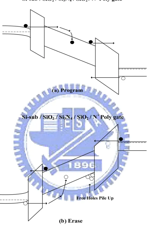
Fig. 2-2 illustrates the program/erase physical operation of a SONOS memory device. In the write operation, a positive voltage is applied on gate electrode relative to the p-type substrate, which forms an electron channel. Then the electrons tunnel through the tunnel oxide into the silicon nitride film and can be stored in deep-level traps. Some electrons which are not trapped in the nitride film will tunnel through a blocking oxide into the gate electrode. The trapped electrons provide the electrostatic
screening of the channel from the control gate, and result in a threshold voltage (VT)
shift. During the erase operation under a negative voltage bias on the gate electrode, the holes tunnel from the substrate into the silicon nitride and are partially trapped in a manner similar to electrons. And some holes “pile-up” at the blocking oxide interface because of the larger barrier height (5eV). Further, trapped electrons may be de-trapped into the nitride conduction band and then tunnel back to the channel. Thus,
for SONOS memory device operation both carrier types are involved in the transport process.
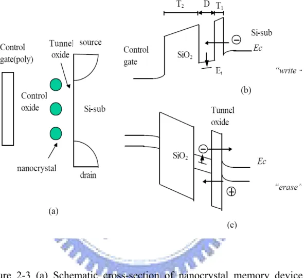
The write and erase processes for an n-channel semiconductor nanocrystal memory device are illustrated schematically in Fig. 2-3. During the write process, a positive gate voltage is applied to inject channel inversion-layer electrons into the nanocrystals. During the erase process, a reverse gate bias is applied to cause the electrons to tunnel back into the channel and the accumulation layer holes to tunnel into the nanocrystals from the channel.
2.2.2 Carrier Injection Mechanisms
(a) Tunneling Injection
Tunneling is a quantum mechanical process akin to throwing as ball against a wall often enough that the ball goes through the wall without damaging the wall or the ball. It also loses no energy during the tunnel event. The tunneling probability, depending on electron barrier height (φ(x) ), tunnel dielectric thickness (d), and
effective mass (me) inside the tunnel dielectric, is express as [2-4]
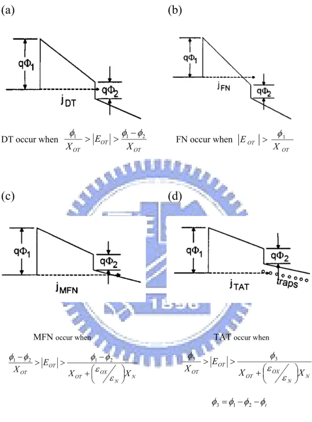
Basically, tunneling injection must to have available states on the other side of the barrier for the carriers to tunnel into. Tunneling through the oxide can be attributed to different carrier-injection mechanisms. Which process applies depends on the oxide thickness and the applied gate field or voltage. Direct tunneling (DT), Fowler-Nordheim tunneling (FN), modified Fowler-Nordheim tunneling (MFN) and trap assistant tunneling (TAT) are the main programming mechanisms employed in memory [2.5-2.7] as shown in Figure 2-4.
Direct Tunneling
Direct Tunneling is the flow of electrons through the full oxide thickness illustrated in Figure 2-4(a). For nanocrystal memories, the control-gate coupling ratio of nanocrystal memory devices is inherently small [2.8]. As a result, F-N tunneling cannot serve as an efficient write/erase mechanism when a relatively thick tunnel oxide is used, because the strong electric field cannot be confined in one oxide layer.
The direct tunneling is employed in nanocrystal memories instead. In the
direct-tunneling regime, a thin oxide with thickness less than 3 nm is used to separate the nanocrystals from the channel. During program/erase operations, electrons/holes can pass through the oxide by direct tunneling, which gives the advantages of fast write/erase and low operation voltage. In the other hand, the direct tunneling is more sensitive to the barrier width than barrier height, two to four orders of magnitude reduction in leakage current can still be achieved if large work function metals, such as Au or Pt [2.9].
Fowler–Nordheim Tunneling
The Fowler–Nordheim (FN) tunneling is the flow of electrons through a triangular potential barrier illustrated in Figure 2-4(b). FN tunneling mechanism occurs when applying a strong electric field (in the range of 8–10 MV/cm) across a thin oxide. In these conditions, the energy band diagram of the oxide region is very steep. Therefore, there is a high probability of electrons’ passing through the energy
barrier itself. Using a free-electron gas model for the metal and the
Wentzel–Kramers–Brillouin (WKB) approximation for the tunneling probability [2.10], one obtains the following expression for current density [2.11]:
⎥ ⎥ ⎦ ⎤ ⎢ ⎢ ⎣ ⎡− Φ Φ = ∗ qF m h F q J OX B B 3h ) 2 ( 4 exp 16 2 3 2 1 2 2 2 3 π 16
Where ФB is the barrier height, is the effective mass of the electron in the
forbidden gap of the dielectric, h is the Planck’s constant, q is the electronic charge, and F is the electrical field through the oxide. The exponential dependence of tunnel current on the oxide-electric field causes some critical problems of process control because, for example, a very small variation of oxide thickness among the cells in a memory array produces a great difference in programming or erasing currents, thus spreading the threshold voltage distribution in both logical states.
∗
OX m
Modified Fowler–Nordheim Tunneling
Modified Fowler–Nordheim tunneling (MFN) is similar to the traditional FN tunneling mechanism, yet the carriers enter the nitride at a distance further from the tunnel oxide-nitride interface. MFN mechanism is frequently observed in SONOS memories. The SONOS memory is designed for low-voltage operation (< 10V, depending on the Equivalent oxide thickness), a relatively weak electrical field couldn’t inject charges by DT or FN mechanism.
Trap Assistant Tunneling
The charge storage mediums with many traps may cause another tunneling mechanism. For example, the charges tunnel through a thin oxide and arrive to the traps of nitride layer at very low electrical field in SONOS systems. During trap assisted injection the traps are emptied with a smaller time constant then they are filled. The charge carriers are thus injected at the same distance into the nitride as for MFN injection. Because of the sufficient injection current, trap assistant tunneling may influence in retention [2.12].
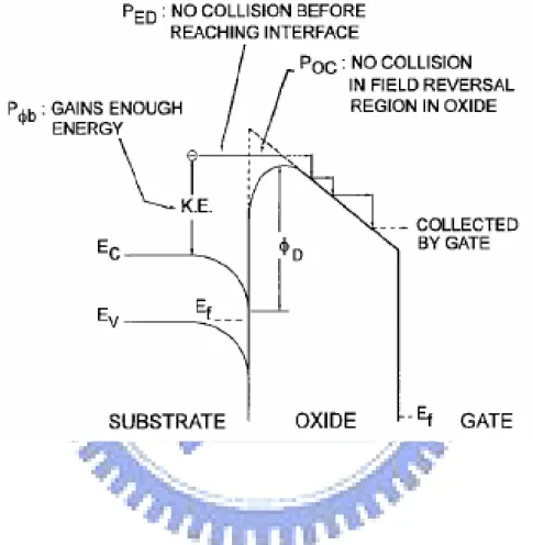
(b) Channel Hot Electron Injection (CHEI)
The physical mechanism of HEI is relatively simple to understand qualitatively. 17
18
An electron traveling from the source to the drain gains energy from the lateral electric field and loses energy to the lattice vibrations (acoustic and optical phonons). At low fields, this is a dynamic equilibrium condition, which holds until the field strength reaches approximately 100 kV/cm [2.13]. For fields exceeding this value, electrons are no longer in equilibrium with the lattice, and their energy relative to the conduction band edge begins to increase. Electrons are “heated” by the high lateral electric field, and a small fraction of them have enough energy to surmount the barrier between oxide and silicon conduction band edges (channel hot electron, CHE). Figure 2-5 shows schematic representation of CHEI MOSFET and the energy-distribution function with different fields. In the other hand, the effective mass of hole is heavier than one of electron. It is too hard to obtain enough energy to surmount oxide barrier. Therefore, hot-hole injection rarely is employed in nonvolatile memory operation.
Nevertheless, a description of the injection conditions can be accomplished with two different approaches. The HEI current is often explained and simulated following the “lucky electron” model [2.14]. This model is based on the probability of an electron’s being lucky enough to travel ballistically in the field ε for a distance several times the mean free path without scattering, eventually acquiring enough energy to
cross the potential barrier if a collision pushes it toward the Si/SiO2 interface.
Consequently, the probability of injection is the lumped probability of the following events [2.15], which are depicted in Figure 2-6
1) The carrier has to be “lucky” enough to acquire enough energy from the lateral electric field to overcome the oxide barrier and to retain its energy after the
collision that redirects the electron toward the interface (PΦb).
2) The carrier follows a collision-free path from the redirection point to the interface (PED).
19
3) The carrier can surmount the repulsive oxide field at the injection point, due to the Schottky barrier lowering effect, without suffering an energy-robbing collision in
the oxide (POC).
(c) Band to Band Tunneling (BTBT)
Band to band tunneling application to nonvolatile memory was first proposed in 1989. I. C. Chen and et al. demonstrated a high injection efficiency (~1%) method to programming EPROM devices [2.16].
Band to Band Hot Electron Tunneling Injection
The injection is applied for n-type substrate nonvolatile memory device. Figure 2-7 shows the energy-band diagram and device operation during the band to band tunneling induced hot electron (BBHE) injection. When band-bending is higher than the energy gap of the semiconductor, the tunneling electron from the valence band to the conduction band becomes significant. The electrons are accelerated by a lateral electric field toward the channel region and some of the electrons with sufficient
energy can surmount the potential barrier of SiO2 like hot electron injection
[2.16-2.18].
Band to Band Hot Hole Tunneling Injection
In p-type substrate, when a negative gate voltage and a positive drain voltage are applied to the cell, electron-hole pairs are generated by BTBT in the drain region, as shown in Figure 2-8. The holes are accelerated by a lateral electric field toward the channel region and some of them obtain high energy. The hot holes inject into charge trapping layer through the tunnel oxide and recombine the stored electrons. This injection is used for a new erase operation for nonvolatile memory device [2.19].
20
2.3 Basic Reliability of Nonvolatile Memory
For a nonvolatile memory, the important to concern is distinguishing the state in cell. However, in many times operation and charges storage for a long term, the state is not obvious with charges loss. Endurance and retention experiments are performed to investigate Flash-cell reliability. In general, NVMs are required to withstand up to 10-100K program/erase cycles (endurance) with 10-year memory retention at temperatures as high as 85 °C.
2.3.1 Retention
Retention describes the ability to the NVM to store and recover information after a number of program cycles at a specified temperature. In any nonvolatile memory technology, it is essential to retain data for over ten years. This means the loss of charge stored in the storage medium must be as minimal as possible. For example, in modern Flash cells, FG capacitance is approximately 1 fF. A loss of only 1 fC can cause a 1V threshold voltage shift. If we consider the constraints on data retention in ten years, this means that a loss of less than five electrons per day can be tolerated [2.20]. Possible causes of charge loss are: 1) by tunneling or thermionic emission mechanisms; 2) defects in the tunnel oxide; and 3) detrapping of charge from insulating layers surrounding the storage medium; 4) mobile ion contamination. Further, the retention capability of Flash memories has to be checked by using accelerated tests that usually adopt screening electric fields and hostile environments at high temperature.
2.3.2 Endurance
21
withstand repeated program cycles and still meet the specifications in the data sheet. In a conventional Flash memory the maximum number of erase/program cycles that
the device must sustain is 105.
A typical result of an endurance test on a single cell is shown in Figure 2-9. As the experiment was performed applying constant pulses, the variations of program and erase threshold voltage levels are described as “program/erase threshold voltage window closure” and give a measure of the tunnel oxide aging. In particular, the reduction of the programmed threshold with cycling is due to trap generation in the oxide and to interface state generation at the drain side of the channel, which are
mechanisms specific to hot-electron degradation. The initial lowering of VT the erase
is due to a pile-up of positive charge which enhances tunneling efficiency. While the
long-term increase of VT the erase is due to a generation of negative traps.
Actually, endurance problems are mostly given by single-cell failures, which present themselves like a retention problem after program/erase cycles. In fact, a high field stress on thin oxide is known to increase the current density at low electric field. The excess current component, which causes a significant deviation from the current–voltage curves from the theoretical FN characteristics at low field, is known as stress-induced leakage current (SILC). SILC is clearly attributed to stress-induced oxide defects and, as far as a conduction mechanism, it is attributed to a trap assisted tunneling, as shown in Figure 2-10. The main parameters controlling SILC are the stress field, the amount of charge injected during the stress, and the oxide thickness. For fixed stress conditions, the leakage current increases strongly with decreasing oxide thickness [2.21-2.23]
22
2.4.1 Quantum Confinement Effect
The quantum dot, is quasi-zero-dimensional nanoscaled material, and is
composed by small amount atoms. The quantum confinement energy dependence on
nanocrystal size has been studied both experimentally and theoretically with the tight-binding model [2.24]. The quantum confinement effect becomes significant when the nanocrystal size shrinks to the nanometer range, which causes the conduction band in the nanocrystal to shift to higher energy compared with bulk material [2.25]. For example, a 3nm Ge nanocrystal can have a conduction band shift of 0.5eV as compared with bulk Ge, which is significant enough to affect the electrical performance of the nanocrystal memory cell.
2.4.2 Coulomb Blockade Effect
When one electron is stored, the nanocrystal potential energy is raised by the
electrostatic charging energy e2/2C, where C is the nanocrystal capacitance, which
depends mainly on the nanocrystal size, though it also depends on tunnel oxide thickness and control oxide thickness. The capacitance is self-consistently calculated using an electrodynamics method [2.26]. The electron charge will raise the nanocrystal potential energy and reduce the electric field across the tunnel oxide, resulting in reduction of the tunneling current density during the write process. It is more dominant at low programming voltages (< 3V). In a flash memory array, device cells often encounter disturbances with low gate voltage soft-programming. The Coulomb blockade effect can effectively inhibit the electron tunneling at low gate voltage and improve the flash memory array immunity to disturbance. However, the Coulomb blockade effect should be reduced by employing large nanocrystal if large tunneling current and fast programming speed were desired. The Coulomb blockade
23
effect has a detrimental effect on the retention time, since the electrons in the nanocrystal have large tendency to tunnel back into the channel if the nanocrystal potential energy is high in retention mode. In the energy band diagram, the Coulomb blockade charging energy only raises the electrostatic potential of the nanocrystal; the quantum confinement energy shifts the nanocrystal conduction band edge upward so that the conduction band offset between the nanocrystal and the surrounding oxide is reduced.
Figure 2-1 I–V curves of the floating-gate device when there is no charge
stored in the floating-gate (curve A) and when a negative charge Q is
stored in the floating-gate (curve B).
Figure 2-2 Energy band diagrams of the SONOS memory device under (a)
program (b) erase operation.● electrons, ○ holes.
Figure 2-3 (a) Schematic cross-section of nanocrystal memory device
structure; (b) illustration of write process: inversion-layer electrons tunnel
into the nanocrystal; (c) illustration of erase process: accumulation layer
holes tunnel into the nanocrystal, electron in nanocrystal can tunnel back
to the channel.
(a) (b)
DT occur when OT OT OT X E X 2 1 1 φ φ φ > > − FN occur when OT OT X E > φ1(c) (d)
MFN occur when TAT occur when
N N OX OT OT OT X X E X ⎟ ⎠ ⎞ ⎜ ⎝ ⎛ + − > > − ε ε φ φ φ φ1 2 1 2
N N OX OT OT OT X X E X ⎟ ⎠ ⎞ ⎜ ⎝ ⎛ + > > ε ε φ φ3 3 t φ φ φ φ3 = 1− 2 −
Figure 2-4 Fourth approaches to programming methods (a) Direct
tunneling (DT) (b) Fowler-Nordheim (FN) tunneling (c) Modified
Fowler-Nordheim (MFN) tunneling (d) Trap assistant tunneling (TAT).
28
(CHEI). The
nergy distribution function at point (X
1,Y
1) is also shown.
Figure 2-5 Schematics of channel hot electron injection
e
29
ergy band diagram describing the process
involved in electron injection.
Figure 2-7 Energy-band diagram for the proposed band to band induce
hot electron injection mechanism and schematic illustration cross of the
Flash memory with p-channel cell. Due to the positive bias to the control
gate, holes are not injected into the tunnel oxide.
N-Sub
P
+ FGP
+V
G< 0
V
D> 0
Figure 2-8 Band to band induce hot hole injection mechanism and
schematic illustration cross of the Flash memory with p-channel cell.
Figure 2-9 A typical result of an endurance test on a single cell.
31
Threshold voltage window closure as a function of program / erase
cycles.
Figure 2-10 Anomalous SILC modeling. The leakage is caused by a
cluster of positive charge generated in the oxide during erase. The
multitrap assisted tunneling is used to model SILC: trap parameters
are energy and position.
33
Chapter
3
Formation, Energy band diagram and Nonvolatile Memory
Characteristics of Manganese Silicate Nanocrystals
3.1 Motivation
Recently, nonvolatile memory (NVM) devices are moving toward high density cell array, low operation voltage, and good reliability. However, the conventional NVM with a floating gate (FG) structure cannot efficaciously prevent data loss in terms of reliability trials for the future scaling down process of tunneling oxide engineering [3.1]. Hence, the next-generation NVM is needed to employ discrete traps or quantum wells as charge storage media to improve retention time. The silicon-oxide-nitride-oxide semiconductor (SONOS) type and nanocrystals (NCs) memory structures have been currently proposed [3.2, 3.3]. In the past few years, many research have shown the high-k trapping layer as the potential candidates for replacing the SiN layer [3.4] , and also demonstrated various NCs to provide charge storage, such as silicon (Si), germanium (Ge ) and metal NCs [3.5,3.6]. Additionally, to use dielectric NC is also investigated by C. H. Chien et al., such as hafnium oxide
(HfO2) and Cerium oxide (CeO2) NCs [3.7, 3.8].
In this study, the dielectric NC manganese silicate (MnSiOx) was successfully
fabricated. It was considered that the charges were stored in the discrete traps of dielectric NCs and the distribution of storage charges were dispersed resulting in a lower Coulomb repulsive force in the charge trapping layer. Therefore, good data retention for the next-generation NVMs will be expected.
34
3.2 Failure Analysis for Fabrication of MnSiO
xNanocrystals
3.2.1 Experimental Procedures
The fabrication of NVM structure was started with a thermal dry oxidation at 950°C to form a tunnel oxide about 5 nm on p-type (100) Si wafer which had been removed native oxide and particles by RCA process, and then a 10-nm-thick
Mn0.2Si0.8 served as a charge tapping layer was deposited by reactive sputtering in the
Ar [24 SCCM (SCCM denotes cubic centimeter per minute at STP)] ambiance at room temperature. Before rapid thermal annealing (RTA) process at 800 °C for 30 s
in the O2 ambiance, the Mn0.2Si0.8 layer was capped by a 10-nm-thick oxide using the
plasma enhanced chemical vapor deposition (PECVD) system at 300°C. The RTA
process was performed to cause the self-assembly of MnSiOx nanocrystal in the
charge trapping layer. After the RTA process, a 30-nm-thick blocking oxide was deposited by PECVD and then deposited Al gate electrodes to form a metal/oxide/insulator/oxide/silicon (MOIOS) structure. Electrical characteristics of the capacitance-voltage (C-V) hysteresis were measured by HP4284 precision LCR meter with high frequency of 1 MHz. In addition, secondary ion mass spectrometer (SIMS) analysis was adopted for the failure analysis.
3.2.2 Results and Discussion
C-V hysteresis is shown in Fig. 3-1 for the MnSiOx layer. From Fig. 3-1,
memory effect is not found in this sample under ±10 V gate voltage operation. On the contrary, leakage phenomenon of the capacitance is clearly observed by (C-V) hysteresis. According to the previous studies, silicon oxide was easily reacted and destroyed by Mn atom. Fig. 3-2 shows the reactive diffusion mechanism of Mn vapor [3.9]. SIMS analysis also exhibits the phenomenon of Mn diffused into silicon
35
substrate in the sputter system as shown in Fig. 3-3.
It is necessary that, before Mn sputtering, a barrier layer deposition avoids Mn direct to interact with tunneling oxide. In this study, we can use a a-Si to avoid Mn react with tunneling oxide.
3.3 Formation of MnSiO
xnanocrystals by RTO process
3.3.1 Experimental Procedures
Fig. 3-4 exhibits schematics of the experimental procedures. The fabrication of NVM structure was started with a thermal dry oxidation at 950°C to form a tunnel oxide about 5 nm on p-type (100) Si wafer which had been removed native oxide and
micro-particles by RCA process, and then a 1-nm-thick a-Si and 9-nm-thick Mn0.2Si0.8
served as a charge tapping layer was deposited by reactive sputtering in the Ar [24 SCCM (SCCM denotes cubic centimeter per minute at STP)] ambiance at room temperature. Before the rapid thermal annealing (RTA) process at 700 °C for 30 s in
the O2 ambiance, the Mn0.2Si0.8 layer was capped by a 10-nm-thick oxide using a
plasma enhanced chemical vapor deposition (PECVD) system at 300°C. The RTO
process was performed to cause the self-assembly of MnSiOx nanocrystal in the
charge trapping layer. After RTO process, a 20-nm-thick blocking oxide was deposited by PECVD and then deposited Al gate electrodes to form a metal/oxide/insulator/oxide/silicon (MOIOS) structure. Electrical characteristics of the capacitance-voltage (C-V) hysteresis were also measured by HP4284 precision LCR meter with high frequency of 1 MHz. In addition, transmission electron microscope (TEM), secondary ion mass spectrometer (SIMS) analysis, and x-ray photoelectron spectroscopy (XPS) were adopted for the microstructure analysis, chemical material analysis of NCs.
36
3.3.2 Results and Discussion
C-V hysteresis is shown in Figs. 3-5 and 3-6 for the control sample and MnSiOx
NCs embedded in SiOx layer, respectively. From Fig. 3-5, memory effect is not found
in the control sample under VG - VFB = ±10 V gate voltage operation. C-V hysteresis
slope is steep, which means the tunneling oxide is less damaged. It’s considered that less Mn atoms react with tunneling oxide due to pre-cap-a-Si layer barrier layer. On the contrary, it is clearly observed that memory windows of 1 and 2.5 V can be
obtained under VG - VFB = ±10 and ±15 V gate voltage operation for the MOIOS
structure with NCs, as shown in Fig. 3-6.
The current density-voltage (J-V) characteristics of different MOIOS structure by gate voltage sweeping from 0 V to 10 V and 0 V to -10 V are shown in Fig. 3-7. It is
clear presented that the leakage current of the memory structures containing MnSiOx
NCs is significantly reduced as compared to that of control sample. This result can be explained introducing the coulomb blockade effect.
The cross-sectional TEM analysis of the control sample is shown in Fig. 3-8. It is obviously observed that less Mn react with tunnel oxide during the sputter process. Secondary ion mass spectrometer (SIMS) analysis also exhibits this evidence in Fig.3-9. Fig. 3-10(a) shows the cross-sectional TEM image relative to the C-V
characteristics of MnSiOx NCs embedded in the SiOx layer. From the plane-view
image of TEM analysis in Figure 3-10(b), the diameter of the NCs is approximately
8-10 nm and the density of the NCs is estimated to be about 8.09×1011 cm-2. The
crystallized NCs with obviously visible lattice images are evident in the insets.
In our work, the chemical composition of the NCs is demonstrated by XPS analysis using an Al Kα (1486.6 eV) x-ray radiation, as shown in Fig. 3-11. Fig. 3-11(a) exhibits the XPS Mn 2p core-level photoemission spectra that indicated the
37
(lower than 640 eV) [3.10]. The O 1s peak shows Mn silicate centered at 531±0.2 eV from Fig.3-11(b) [3.11]. According to the previous research, Mn oxide is centred at values lower than 530 eV [3.12]. It was believed that the main component in this trapping layer was Mn silicate.
We considered Gibbs free energy values, the actual value for chemical reactions
involving Mn silicate and SiO2 formation. Some allowed chemical reactions are listed
below[3.13, 3.14].
Si + O2 → SiO2 ΔG298K0= -732.94 KJ/mol (1)
Mn + 1/2 O2 → MnO ΔG973K0= -615.03 KJ/mol (2)
MnO + SiO2 → MnSiO3 ΔG298K0= -1244.7 KJ/mol (3)
MnO + 1/6 O2 → 1/3 Mn3O4 ΔG973K0= -206.34 KJ/mol (4) According to previous studies, Mn preferred forming MnO first. We observed
that among all the thermodynamically allowed processes, MnO would form MnSiO3
rather than Mn oxide.
We are most concerned for the band diagram of MnSiOx. The intersection of two
straight line segments-one fit to the linear portion of the VB leading edge and one fit to the background channels between the VBM and the Fermi level, as determined by the Kraut method, for Si, and oxides [3-15, 3-16]. Fig.3-12 shows the results that the valence-band spectrum of P-type Si (100), 5nm SiO2/ P-type Si(100) and 5nm
MnSiOx/ P-type Si(100) by XPS analysis. The valence band offset between MnSiOx
and P-type Si (100) is estimated to be 2.8 eV.
In dielectric thin films, Plasmons and band to band transitions of XPS signals appear in the lower kinetic energy side of primary core-line peaks by the corresponding loss energy. The energy loss for the plasmon excitation is generally much larger than the energy of excitation from the valence band maximum to the conduction band minimum. Therefore, the band gap values like the high-k dielectric can be determined from the threshold energy of the energy-loss spectrum for O1s and N 1s [3-17, 3-18]. The O 1s photoelectrons energy-loss spectra for 5 nm thick thermal