,111
ELSBVI ER Thin Solid Films 290-291 { 1996) 458-a63
Effects of mechanical characteristics on the chemical-mechanical
polishing of dielectric thin films
Wei-Tsu Tseng a,,, Chi-Wen Liu b, Bau-Tong Dai a Ching-Fa Yeh ~
• NationaINano Device Laboratories, I001.1, Ta-Hzanh Road, Hsinctu¢ 300, Taiwann Taiwan Semiconductor Manufacturing, Company, N~incka, Taiwan
¢ Departmeat oJElectmnic.¢ Engineering and/#sliture of Electronic.r, National Ckiao-Tung University, IOOL Ta.Hsueh Road. R~inchu, Talwan
Abstract
']'he effects of as-depo;ited (intrinsic) stress, externally applied (extrinsic) stresses, hardness, and modules of various dielectric films on chemica]-machanical polishing (CMP) removal and post.CMP cleaning processes are studied in this article. Intrinsic stresses of the polished dielectrics do not contribute directly to the CMP removal rate. Extrinsic stresses including normal and shear components are caleulatedusing principles of elasticity and fluid mechanics respectively and their roles in the material removal process are discussed. Theoretical evaluation and experimented results both suggest thai hardness and modulus are the two most important material characleristic5 affecting the CMP process. Efficiency of post-CMP particle extraction can be monitored using an adhesion probability which is related to the hardness of wafer and pad. In addition, particle removal rote can he remarkably enhanced by increasing pressure thermal stress) white increasing pad rotation speed (shear stress) contributes little to reduce the particle count.
IfeywoMs: Chemiesl-n~chanical polishing; Hardnesa; Stress: Dielectrics
1. Introduction
The shrinking dimensions of devices to increase packing density for the IC technologies of future generations (0.35 ~m or less) impose, greater demands on the planarization process. This results from the lithographic need for steppers with reduced depth of focus which inherently enforces a more stringent requirement for flat and planarized surfaces, Among the newly developed plaparization technologies for ULSI metallizations, chemical-mechanical polishing (CMP) has been shown to be the most promising because of its demonstrated capability to provide better local and global planarization of wafer surfaces in multilevel metallization imereonneet structures for advanced IC devices [ 1,2].
During CMP of dielectrics, material removal was achieved by the relative motion of the wafer and the pad on which u proper slurry is dispersed. The miss of the slurry are both to chemically attack the dielectrics and to mechanically deform the polishing surface. Hence, the surface mechanical prop- erties of polished films have great influ©nee on the wear mechanism during CMP processes. In addition, the particle removal process through rubbing or scrubbing actionsduring
~' CortespeMlng author. Tel: ÷ 886-35.726100 est. 7717. Pat: ÷ 886- 35-?l 3403..~.mtil: Wrtv.~ @~t.n~tu.edu.lw.
0040-60~196/$18,00 ~ 1996 Elsevier Science S,A. All rlg~ reserved
Pll$OO4o.a090(96)09020.')
post-CMP cleaning depends much upon the adhesion forces between particles and wafer surface and hence the mechanical nature of s0rfaee of the dielectrics [ 3]. Thus, there is a need to study the correlation between the mechanical characteris. tics of the dielectric films and the variations in the material removal rate during CMP and in the particle removal effi- ciency during post-eMP cleaning.
The goat of this study is to elucidate the roles of common mechanical characteristics in the material removal and the post-CMP particle cleaning processes, Emphasis on the eval- uation of the contribution of and correlation between stresses, both intrinsic and extrinsic, hardness and modulus in a di- electric CMP process. Since, for most of tit,: covalent-bonded materials, a tensile stress corresponds to bond stretching whereas a compressive stress translates to bond contraction in the structure, the surface of the dielectric materials being polished may have ~ e n weakened or streugthaneddepen4ing on the state of their intrinsi~ stresses, In fact, silicon dioxide has been found to relax its tensile stress by cracking [4J. Thus the existence of such intrinsic stresses may assist or retard the material nutting process to certain extent. On the other hand, during u CMP operation, the imposition of a down force and a pad rotation exerts on the wafer additional normal and shear stresses respectively, These stress components are din2ctly related to the CMP removal rate as Preston's law
• .T 7~eng ¢1 aL IZ~in Solid Filma 290-291 (1996) #3g-463 459
prescribes [5,6], Nevertheless, how these extrinsic stresses, combined with the life.mentioned intrinsic stresses.interact in a way to manipulate the CMP removal process remains
obscure and is worth investigating,
From another perspective, hardness is the resistance of a ma~rial to plavic deformation which consistently gives an index of strength and structural coherence, The modulus of elasticity quantifies the elastic response of a material under
static loading, Both of these quantities reveal the material's
response to external much .anical perturbation and would be more infallible material indicators fur CMP process control, Our previous work [7] found experimemully u linear zela- tionship between the surface hardness and the removM rate
of oxide films. Theoretioal assessment on this observation is still lacking however and further work is needed to justify that point, Finally, the effects of the above mechanical char- acteristics on post.CMP cleaning process have rarely been addressed in the literature and deserve further investigation. We will investigate the above issues based on existing models
and our own experiments,
:~, Experimental
All test samples in the present study were grown on P-type (100), 150 mm silicon wafers, Thermally grown films of
silicon d{ oxide were aceomplished by wet oxidation, in which the silicon was exposed to the oxidizing ambient Hz, O~ at 980 °C. Films of atmospheric pressure chemical vapor dep- osition (APCVD) and plasma-enhanced chemical vapordep-
osifion (PECVD) oxide were deposited by reacting Sill 4 and 02 at a temperature of 400 aC. TEOS and 02 at 390 eC were used as reactant gases for TEOS,PECVD films while Sill.., N2 and NH3 were used for deposition of SisN4-PECVD films. Silicon.rich oxide films (SRO-PECVD) films were obtained in ambient SiH,~, N~ and NzO gases,
All experiments were carried out on a Westech 372M pol- isher with an IC 1000/Su~ IV pad pre-wetted with CAB-O- SPERSE SC-1 slurry consisting of fumed silica particles sus- pended in alkali solution, Upon the completion of each polish,
pad conditioning was performed to clean the pad of n:sidual
slurry and to lift the pad surface fibers for f, rther processing. The thickness of dielectric films was measured with Nano- metrics 2100XP at nine different spins across the wafer, The polish rate is defined as the removal rate averaged over the nine locations, The cross-wafer polish non-uniformlty was less than 10%, In order to eliminate the run.to.run removal rate variation, the removal rate ratio (RR ratio) is defined as: RR ratio = (removal rate of dielectric filmi /
(removal rate of thermal oxide)
Intrinsic stresses of dielectric films ,~ese monitored from
measu~d curvature change. The intrinsic stresses of most dielectric films ure compressive while that of SiH,-APCVD is tensile. A NANOTEST 500 indentation system with a
B arkovich indenter was used to measure nanoscale hardness, All tests were pertormed at a nominal constant loading rate of 1.18 mN s "v until u maximum
displacement
300 nmreached. The pH of the dip solution for post-cleaning was
adjusted by adding NH40H and HCL to D.I, water, The numl~r of particles (>0,2 i~m) on the POsI-CMP wafer surface was counted with a TENCOR-4500 surface scan.
3. Results and discussion
3,1. Thecorrelalionbetweenmeckanica/characlertstic8 and eMP removal rate
The dielectric CMF process has much in common with glass polishing. Cook [5] reviewed the mechanics of glass
polishing and proposed that removal rate is inversely pro- portional to the modulus, E, of glass, The theoretical work by Liu et el. [ 8] also deduced that the removal rote depends on the meduli of both abrasive particles and the film itself, Nanohardness of dielectric oxide films has been found to scale down with CMP removal rate [8] whereas the exact mechanism remains obscure, Correlation between filmresid- unl stress and removal rate have been reported [9.10] although proper explanations are still lacking.
In this section, an attempt will be made to clarify the roles of stresses {both extrinsic and intrinsic), modulus, and hard- hess in CMP removal process based on themetical calcula- tions as well as experimental data.
3,1. L Extrinsic stresses of the dielectric films during CMP Runnels and Eyman [6] considered a mum general removal m~id analogous to Preston's equation:
RR=£X~r.Xv (I)
where k is the proportionality parameter and o'p and v are the normal' and shear stresses on the wafer surface respectively. Thenormal stress originates from the down force imposed by the polish arm onto the wafer tan'tar white the ~hear stress
arises from sluny flow generated by the relative rotational motion of platen and wafer carrier. In this article, o- A and ¢ arc termed extrinsic stresses while the as-deposited stresses of the thin films are called intrinsic stresses.
Under a CMP down force P. the pad is deformed and the
size of the pad surface features (or "valleys") become
smaller; therefore, mote silicaparticles caneffectivelyabtade the film surface, This process apparently has contribution to the modified Preston equation presented above. Cease. quently, the normal stress is actually applied to the wafer through direct contact between the polished wafer surface
and the abrasive particles, Cook 15 ] reviewed the mechanics.
during glass polishing which can be applied to the case of
CMP, In his model, impingement of abrasive particles trans.
ported by the slun'y leads to Hertzian penetration of the sur~ face, The CMP process can be perceived us a travelling indenter whose interaction (contact) with the wafer surface
460 W.. Z T:mn~ et at, / Tkin oe olid Fil,,e.~ 290,..2@ ~ (I 996) 45~-463
gives rise to bond weakening and hence atomic removal, The force Fasting on a particle ofdhmeter d in the particle/wafer contact is expressed as:
= 2 g (2)
where Kis the abrasive fill fraction which is unity for a fully- filled closed packing. Assuming spherical particles, the con- tact area between the polishing particle and the polished material surf~ee is 'nr~c, where the radius of contact is given
by:
( 3 "1 Its
rcffi~.-~F(d/2)[(l-v2)/F.+(l-v:')/E'] ~
(3) where d and E' are the Poisson's ratio and elastic modulus of the polishing particle respectively. Given Eqs. (2) and (3), the normal s~ess o-, can be calculated:F
~. = ~ (4)
The basic specifications of the SC-1 slurry used for thi: study is listed in Table 1. The solid concentration of the slurry is reduced to 11,25 wt,% after being diluted by two (volume) parts of D.L water, Assuming K=0,5, v=d=fi.03, £ = E' = 70 GPa [5] and a down force of 7 psi (48 260 Pa), the calculated normal stress based on Eq. (4) is about 46
MPa,
Runnels [ I l ] relates the feature-scale erosion rate to Pres- ton's equation by simulating the stresses due t~ slurry flow. In his model, the sbear s ~ s s fcan be approximated as:
~/ttV/PA/
where p is the dynamic viscosity, V is the pad velocity and A the wafer surface area. The calculated shear stress based
on Eq. (5) and the parameters in Table I is about 170 Pa, or
five orders of magnitude lower than the normal stress!
The large disparity between the normal and shear stresses seems surprising at first given the modified Preston' s equation that the removal rate is proportional to both of them as indil cated in Eq. ( I ). The roles of the two stress components in the remove[ process are different however and may not be compared on the basis of their magnitude. The normal stress acting on the travclling indenter (particle) gives rise to a
Table I
Speclflcntlnns of SC-I slum/
pX (adjusted with KOH) 10.0~ 10,3 Specific gravity 1.198:i:0.0]2
Vlsco~ity < 150 eps
W=ight per'gallon IO,O±O,I
w,.% aotkb 30.0 ± 0.3
Noml~ plni¢le si~ ~Onm
compressive zone extending from the leading edge and a eonespo~ding tensile zone extending from the trailing edge, hence contributes dire ~tly to the bond breaking of the pol- ished material. While, on the other hand, the shear stress signifies the speed at which the removed material gets carried away by the flowing slurry. Both of the processes combined contribute to the effective removal of material during CMP operation.
3.1.2. Effec:s of intrinsic stresses
The intrinsic stresses for various dielectric films and their effects on the CMP removal rate are presented in Fig. L For all the SiO2-based dielectrics, no distinct correlation between the intrinsic stress and removal fate can be identified. The bond stretching or contraction doe to tensile or compressive stresses respectively in the oxide network apparenflycontrib. utcs little to assist or to impede the material removal process during CMP. However, one study [9] found acorresponding increase i,J CMP removal rate with increasing compressive stress in SiN~ films as the films become more silicon.rich. Another recent investigation [IC'] identified a linear relation- ship existing between the intrinsic stress (from high com- pressive to low tensile) and CMP removal rate for fluorinated oxide (SiOF) films.
The above contradiction may be rationalized on the basis of the enhanced chemical effects during CMP. In the present study, the stoichiometry for the various oxides does not alter and the O-Si--O bonding configuration remains essentially the same except for a few impurity species embedded in the network due to different processing gases, For the silicon nitrides however, the films become silicon rich as stress increases. The variation in ~toichiometry may have altered the bonding and the chemical etching rate of the nitride there- fore the chemical erosion rate during CMP is enhauced. The same reasoning can be applied to account for the CMP rate increase in fluorinated oxides. The shift in stress towards the tensile side also corresponds to increases in wet etching rate and fluorine concentration [ 10]. The presence of the highly cloctronegative fluorine not only changes the config~ation of the oxide network but also increases the hydrophici[ity of the films. The intensified water permeation combined with
J 1.o d • |o0 .lee fl • b I s l s N l 4 q e ~ A s u ~ q l ~ A ~ S 111 leo Film Ot~ee (MPa)
W,.Z Tseng et al, I Tkin Sol(d RIms ~90..2'9t (1~) ,/58~63 461
the formation of the corrosive HF radicals are directly respon- sible for the enhanced CMP removal rate [ 12] which coin- cides with the stress changes in the fluorinated oxide films.
The magnitude of the intrinsic stress for most oxide films resides ia the range of 1~~300 MPa which is far less than their tensile strength t 5D00~ 7000 MPa). Therefore, assum- ing minimum cracks or other atress raisers in the oxides, the intrinsic stress weuld contribute little, if any, to the breaking of the hands. Also worth noting here is that the calculated normal stress (46 MPa) is about two orders of magnitude lower the tensile strength, In Cook's model [5], the maxi- mum tensile stress in the tensile zone trailing behind the moving particle is only around 200 ~ 300 MPa to the best of approximation, How these stresses surmount the tensile strength to break the materials away hence becomes an intriguing question. The formation of a soft surface layer, possibly in hydrated form, due to chemicalatta~k by the slurry may provide an explanation to the above scenario, The exact mechanism would not be clear however until knowledge on the chemical aspect of the CMP process improves.
3.2. Effects of hardness and modulus on removal rate While stress provides only static-state information of a material, hardness reflects the resistance of a material toplas- tic deformation and hence provides more information on the deformation and wearing of the materials themselves The analogy of a moving particle to a traveling indenter adopted by Cook in his model suggests that hardness may be a more useful material index to monitor CMP removal rate, On the other hand, the application of elasticity theory to model polish mechanics as presented by several previous studies [6,13] implies that elastic modulus may play certain role in the polishing operation. Since most of the dielectric materials undergo only elastic deformation before fracture, the mag- nitude of their elastic modulus may have some correlation with their CMP removal rate.
Our previous work [7] found that the polishing rate of the various dielectric materials is inversely proportional to their hardness except for PECVD SisN4 whose removal rate rests above the fitted RR vs. hardness line (Fig, 2). This discrep- ancy can be explained on the b~is of the different mechanical characteristics between the abrasive particles and wafer dur- ing polishing as discussed below, Cook's theory [5] and the wear model by Li~z ~.t al. [ 8 ] have both correlated the removal rate with mechanicm properties of the wafer surface and abra- sive particles:
RR = C ×
(
I/E, + I/E~) X ? × V(6)
where E, and E. am the elastic medals of the abrasive parti- cles and the wafer surface, respectively, C is u constant relat- ing chemistry to material removal process.
Gilman [14] has shown that the micmhardness of struc~ turel materials increases linearly with an increasing modulus, and the berdness-to-mndulus (H/E) ratio is about I/10 for
t . S '
,It, W
~ S . . . .
O,S 1 . 0 1 . S ~l,a
Hardnus Ratio
Fig. 2, Effects of film hardness on CMP removal ra~¢ for various dielc, c~cs, must cov~lendy bonded solids, Thus Eq. (6) can be trans- formed into
RR=C' x ( t / H , + l/H.) x P x V (7) where H, and H,,, are hardness of the .~brasive particles and the wafer surface, respectively. C' is ~, constant, Therefore, as Eq. (7) indicates, a linear relationship, exists between the surface hardness and the removal rate o1: oxide films under well-controlled CMP processes.
On the other hand, the basic structure of silicon nitride consists of a SiN, tetrabedron shared by three other SiN4 tetrahedru m form a three-dimensional network. This creates the exceptionally strong bonding in SiN, producing a very rigid structure with a Young's modulus greater than three times that of quartz, in which the oxygen atom in $iO forming a silicate network share only two temthedru [ I5 ]. In addition, the chemical nature and corrosion susceptibility of astride and oxide arc different. Thus, the combined mechanical and chemical differences gives rise to the removal rate dcviaGon of nitride from those for oxides in Fig, 2.
3.3. Ef/ects of mechanical properties of dielectric films on particle removal
Particle contamination on a wafer surface often causes a dramatic decrease in device yield. Much work has been don~ to describe the panicle deposition mechanism with the inten. lion to minimize the number ,3f metal cont~'ninants, residual chemicals and other foreign particles remained on water sur- face [16]. Post*CMP cleaning is often achieved through mechanical brushing or scrubbing actions aided with proper chemicals to "dissolve" the particles away. It has been reported that the sign and magnitude of the zeta potentials between sluny, wafer surface and pad play critical roles in the particle deposition/extraction processes on the wafer sur- face [ 17]. However, measurements of the zeta potential on the wafer surface exhibit complex dependence on pH, type of chemical, method of POst-CMP cleaning, wafer rotation speed, water flow rate, and other machine parameters, and therefore is not considered a quick and efficient way for process control,
Since particle removal by mechanical brushing and scrub. bing actions resembles much of the material removal process
462 W,.; ', 7~ug et at, / Thil= Solid Flinty 290-291 (I 9~6) 458-463 ~ sou0 s g.qkl,PSCVD 0 ' f ~ l OliMs D IkII~PlCYD 4000, i ~L o 2000' #
!
|
Z o,s 1.0 1.s 3,0 Hnrdneaa RatioFig, 3, Th~ number of panicles remaining on the pOsl.CMP wLfer surface versus dim hardness after 30 rain dip at solution with pH = I0.
in CMP, the mechanism of post-CMP cleaning may exhibit similar dependence on the mechanical characteristics as dis- cussed in the previous sections. In fact, the adhesion force [ 18] between particles of polished dielectrics and the dean- lag pad is related to their hardness and hence can be an important indicative for the ease of particle removal, This point will be elaborated in this section. In addition, extrinsic stresses which are feared to dominate the CMP removal proc- ess will be investigated again with the intention to clarify their roles in the post-CMP buffcleaning proce~,s.
3.3.1. The effects of hardnest on parlicte removal process In order to examine the effects of film hardness on particle removal for polished wafers, post-CMP wafers are directly transported from the unload cos sette to u tub with dip solution. Fig. 3 indicams that less particles would remain on the harder (nitride) wafer surface after 30 rain dip at the solution with pH = 10. This phenomenon can be justified from the stand- point of "adhesion force" since the probability ofadberence of particles on polished film (/3) is related to the hardness of the pad surface (Hp) and of the polished film (Hf) [ 18]:
afHp/tHr+Hf> (8)
For dielectric materials, the wafer surface is hard and brittle, while the pad, typically polyurethane-based materials, is much softer. Hence, Eq, (8) can be simplified as:
a=n~/nr
(9)Eq. (9) suggests thattbe probability of particles physically embedded on the wafer surface is inversely proportional to the hardness of the polished film, i.e. particles can be removed more easily from the harder surface. The existence of hard- ness terms in the expression for ndbesior, probability implies that particles, are Or, dented into the wafer surface. Thus the mechanism of its removal would bear the similar dependence on material churacteristiesdiseussed in Section 3.2.
Eqs. (8) and (9) give qualitatively the relative ease of particle removal and should be applied wlth caution. Hard- ness alone may not be enough to monitor the partiole removal prates,. Fc,r further study, additional material characteristics
such as surface roughness (of wafer and pad) would be needed to modify Eq. (8),
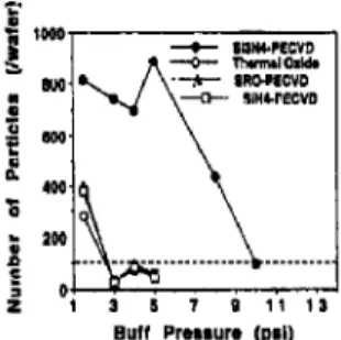
332. E~ects of exfrln~ic stres,~es on particle removal In-sire removal of parth.les on the post-CMP wafer surface via an applied pressure was carried out on the cleaning platen. Each polished wafer was subjeoted to 30 s of mechanical buffing with a Rod¢l finishing pad (Politex Supreme Regular Nap). Deionized water was applied during buffing, and both carrier and platen were rotated at 60 rpm. As Fig. 4 indicams, the final particle counts can be reduced significantly by increasing pressure. Based on the experimental results, the particle removal efficiency is tbund to be greatly improved by increasing pressure to 3 psi for undoped oxide and I0 psi for PECVD-nitrido film, respectively In contrast, post-buff- ing particle count is plotted against pad rotation speed in Fig. 5 w~th pressure and carrier speed set at 3 psi and 60 rpm, respectively. Unlike the polishing process, the particle level the on wafer surface is almost independent of pad speed. The above results clearly indicate that normal stress ,'elated to pros sure plays a much m ore important role in particle removal than shear stress related to platen and carrier rotation speeds, While the concept of indentation can be applied to both mate- rial polishing and particle removal processes, the latter does not involve material catting actions however and this may provide an explanation to the different behaviors between the
':!
400- c I SlIM4.1~¢VD ' i - ' O ' - - ~ all elide - ,-'-~4~ |RC4ZICVC •IH&rECVD 3 S 7 9 11 1 Buff Pressure (pli)Fig. 4. Effucts uf buff pr~snn~ on the number of panicles remaining on the post-C'MP wafer surface, Parliele count tess then 100 pcrwQ1~r is ¢onsLdeNd a viabtc cleaning process,
al NO' I _Q = SO0 I 400 ¸
!-
t I e liglH4.pecvo --.o-- TMm~ C~dQ ----k-- |RO#IICV9 IHH44q[CVD so co Io 1so 1so l i e Second Pl|fen $1~HKI (rpm)W..T. Txerlg et al. / Th~n S~lid Filrn,~ 290-29/{ 1996) 458-463 463 two processes. During polishing, a shearing action is needed
-to peel off the indented malerial whereas during particle removal process a large enough applied pressure overcomes the adhesion at~d electrochemical forces, plowing the parti- cles off from the wafer surface without physically tearing apart the adjacent materials.
4, Conclusion
The effects of extrinsic stresses, intrinsic stresses, h~dness and modulus of various dielectric films on the CMP removal process are examined theoretically and experime,,tally. The calculated extrinsic non'nat stress is about five orders o f ~ a ~ - nitude higher than extrinsic shear stress and it would be expected that both of them contribute remarkably to the ma~,e- rial removal during CMP. On the contrary, intrinsic stress plap: little role in the polishing process. Correlation between intrinsic stress and CMP removal rate identified in other stud- ies may arise from chemical interactions between slurries and wafers. The material removal process during CMP cnn be perceived as a moving indenter across water surface. Removal rate of dielectrics is inversely proportional to the combined hardness of dielectrics and abrasive particle~. An adhesion probability related to material hardness can be used to indicate the relative efficiency in post.CMP particle removal. Finally, normal stress (pressure) is found to dom- inate over shear stress (rotation speed) in the particle reduc- tion on the wafer surface.
Acknowledgements
This work is financially supported by TSMC, ~nd National Scieocc Council (NSC84-2622-E009-007) of Taiwan.
References
[I] W.L Pa~ck, W.L. Guthd~, C,L. Stmdley and PM $¢hiabl¢, J.
Elccl,"~¢hcm. Sac,, ]38 ( 1991 ) 1778.
[2] W.L. Gulhde, W J, Patrick, E Lavlne, H.C, Ionos, EA. Meht~r, T.F. Houghton, G.T, Chili and MA, Fury, I t M ], Res. De velop., J6 ( | 992 )
845,
13] ]r), H,call~dagton, P. Resnick, R. Timon, B. Ural~r, M, Ravkia, J, DeLarina, W. Kru~n and A. Madhaat. Pr,~c. Dielectrics for !'L~[/
ULS! Mattilevd htercoanee* C'oaf, VMIC, Tampa, FL, USA, 1995, p. [56.
[4] A.K. Sinha, H..L Legit;stein and T, PI Slaith, J. Anpl. Pl~,s.,,19 (1978) 2423.
[5] L.M. CooR, J, Noa-Cry~f. Solid,, 120 (1990) 152,
[6] S.R. Runnels and. L.M. r:yman, J. E[eoroehem. gee., 141 (199¢) 1698. [7] C..W. Li,J, B ,-'[', Dal and C..B. Veh,). El¢ctrcchem. Sac., 142 (1995)
3098.
[8] c..w. Liu, B...". Dai, W.-T. T~;eng a ~ C.-F. Ych, .~ Electrocl~em.
See., 143 t t996} 71~.
[9] B.-T. Did, W.-T. Tseng, C.-PI. Liu and C.-F~ Yeb, Prec. SEMI ~'aiwan
Techaica~ Syrup,, SEMI, Mo~nW.itl View, CA, USA, 1995, p, 105, [ tQI C.-P, Cl',¢n, C,-T. Lee, C,-F. Lin, H..-C. Yung and L. Fang, Prae. Ist,
Inc CMP Planarizalio~ for VLSI/UL3I Mutlilevet larrrco~,ectio~ Con:,, VMIC, Tampa. FL. USA. 1996, p. 82.
[ I I ] S,R. Runnels, J', Becrruchern..%c, 141 (1994) I~O0. [ 127 Y.-T. Hsieh, W..T. Tsang, B.-T. Dai, T..C, Chang, Y,-L Mei, J,-D,
Sl'¢u, C.-F Lia and M.-S. Funk. Proc, 2nd~ hit, Dieteetr~csfar VI.,$1! ULSI Marrile~el h:tercoanec: Con~, VMIC, Tampr,. FL, USA, 1996, p. 287,
[ 131 T. Izumttani, in M. Tomoxawa ,rod R. Do,"emus (eds.), T~lise oa
Materiah Science and Teehnatojty, Vol. 17, Academic P~s, New York, 1979, p, 115,
[ 14] l.l. Gilman, Mechanical Behavior Of Cy#latlioe .¢,tidJ, Nalioa~ Bureau of Standards Moao/Iraph, Vo[. 59, Gaithersb,tg, MD, USA, 1963, p, 79,
[ 15 ] J,A, Taylor, 1 Vat. Sd, Tec/~vL, A9 { 1991 ) 2464,
[ 16] W.C Krusell, J.M. de Larios and J. Zlmng, SolidSrate T¢cl~ol,. 38 (6) (1995) In9.
[1"/I TL. Myers, M.A. Fury and W.C Krnsell, Solid Strut Teclmtd,, 38 (I0) (19~5) 59,
[ 18] I.V. Kragelsky, M.N. Dobychih and V.S. KOlhbidov, Friclifm a,d