89
Effects of Ni Thickness and Reflow Times on Interfacial
Reactions between Ni/Cu Under-Bump Metallization and
Eutectic Sn-Pb Solder in Flip-Chip Technology
CHIEN-SHENG HUANG,1JENQ-GONG DUH,1,4YEN-MING CHEN,2and
JYH-HWA WANG3
1.—Department of Materials Science and Engineering, National Tsing Hua University, Hsinchu, Taiwan. 2.—Department of Materials Science and Engineering, National Chiao Tung University, Hsinchu, Taiwan. 3.—Chunghwa Telecom Co., Ltd. Yang-Mei, Taoyuan, Taiwan. 4.—E-mail: [email protected]
Flip-chip interconnection technology plays a key role in today’s electronics packaging. Understanding the interfacial reactions between the solder and under-bump metallization (UBM) is, thus, essential. In this study, different thicknesses of electroplated Ni were used to evaluate the phase transforma-tion between Ni /Cu under-bump metallurgy and eutectic Sn-Pb solder in the 63Sn-37Pb/Ni/Cu /Ti/Si3N4/Si multilayer structure for the flip-chip
technol-ogy. Interfacial reaction products varied with reflow times. After the first reflow, layered (Ni1–x,Cux)3Sn4 was found between solder and Ni. However,
there were two interfacial reaction products formed between solders and the UBM after three or more times reflow. The layered (Ni1–x,Cux)3Sn4was next
to the Ni/Cu UBM. The islandlike (Cu1–y,Niy)6Sn5 was formed between
(Ni,Cu)3Sn4 and solders. The amounts of (Cu1–y,Niy)6Sn5 intermetallic
com-pound (IMC) could be related to the Ni thickness and reflow times. In addi-tion, the influence of Cu contents on phase transformation during reflow was also studied.
Key words: Flip chip, under-bump metallization, intermetallic compound,
diffusion, phase transformation
INTRODUCTION
Flip-chip technology with the aid of ball-grid array interconnection has attracted a great amount of attention in today’s electronics packaging. It pro-vides many excellent advantages, such as a large number of input/output connections, good electrical performance, easy assembly, and high reliability.1–3
One of the challenging issues is the material selec-tion for under-bump metallizaselec-tion (UBM). Because of the rapid reaction of Sn with Cu, and the spalling effect of the Cu-Sn intermetallic compound (IMC), the Cu-based UBM has been found to be incompati-ble with SnPb solder or high melting-point sol-ders.4,5The Ni-based UBM is of interest in flip-chip technology because of the slower reaction rate with Sn in solder; thus, the spalling of the Ni-Sn com-pound will be limited.6
In the literature, most studies were focused on
solders with Ni-based UBM during liquid-state an-nealing, i.e., annealing above the melting point for several minutes or hours.7–11However, the dwelling time, i.e., the total time of temperature above the melting point for real reflow process is less than 100 sec. That is to say, the associated reaction between liquid-state annealing and soldering reflow should be quite different, owing to the distinction of time duration. It is, thus, interesting to evaluate the in-terfacial reaction between PbSn solder and Ni/Cu UBM during multiple reflows. In this study, a 63Sn-37Pb /Ni /Cu/Ti/Si3N4/Si multilayer structure was
used. Titanium played the role of the adhesion layer, and Cu was the conductor, while Ni acted as the wetting layer and the diffusion barrier. Different thicknesses of Ni (1 m, 3 m, 5 m, 6 m, and 9 m) and multiple reflow (1, 3, and 5 times) were car-ried out. According to the compositions of IMCs eval-uated in the joint, the phenomenon of phase trans-formation during soldering reflow could be studied.
90 Huang, Duh, Chen, and Wang
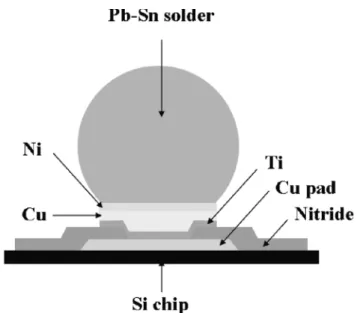
Fig. 1. The schematic illustration of UBM.
EXPERIMENTAL PROCEDURE
Figure 1 shows the UBM structure used in this study. The top metal of the Si wafer was Cu, which acted as an interconnection line. The adhesion layer was sputtered Ti of 1,000 Å. Then, 5,000-Å Cu was sputtered on Ti for electroplating seed layer. The electroplated Cu was further deposited on the met-allized substrate. The thickness of the electroplated Cu was 5 m. Nickel with different thicknesses was electroplated on the top of the electroplated Cu. The thicknesses of Ni selected in this study were 1 m, 3m, 5 m, 6 m, and 9 m. After UBM was plated onto a Si wafer, the eutectic Sn-Pb solder bump was then electroplated. All metal films were deposited consecutively without breaking vacuum.
Solder reflows were conducted in an infrared solder-reflow oven. The peak temperature and dwell-ing time of the reflow profile were 225°C and 70 sec, respectively. The cycles of solder reflow were one to five.
The surface morphology of electroplated Ni was characterized by an atomic force microscope. The interfacial morphologies between Sn-Pb solder and UBM were analyzed with a scanning electron micro-scope. The compositions of phases in the solder joints and elemental distribution across the joint interface were quantitatively measured with an electron probe microanalyzer (EPMA) with the aid of the ZAF correction program.12
RESULTS AND DISCUSSION Interfacial Reaction between PbSn Solder and Ni/Cu UBM
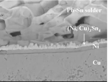
Cross-sectional images of the Pb-Sn solder/Ni interface after one reflow are shown in Fig. 2. The thicknesses of Ni were 1 m, 3 m, 5 m, 6 m, and 9 m, respectively. Only one layer of IMC was found between solder and Ni in all joints after one
reflow. The reacted layer was less than 1 m. In the case of 1-m Ni, the composition of the reaction product was 57.5at.%Sn-36.4at.%Ni-6.1at.%Cu. The IMC size is close to the detection limit of the EPMA if the resolution of electron probe size is considered. To obtain the quantitative data more precisely, a detailed and deliberative task was car-ried out in the EPMA analysis by controlling the appropriate accelerating voltage, beam current, and focus-beam size. The reported compositions as listed in this study were, in fact, the average of at least 10 measured points. The ratio of the atomic percentage of (Ni ⫹ Cu) to Sn was (36.4 ⫹ 6.1): (57.5), which is close to 3:4. Thus, this IMC could be denoted as (Ni1–x,Cux)3Sn4. A similar observation
was reported recently in the literature,13–15yet the concentrations of Cu in Ni3Sn4 were all different.
In the other cases of different Ni thicknesses (3 m, 5 m, 6 m, and 9 m), the reaction products were also identified as (Ni1–x,Cux)3Sn4. However, the
val-ues of x in (Ni1–x,Cux)3Sn4were different, as
repre-sented in Fig. 3 after detailed composition analysis by EPMA. As the thickness of Ni increased, the val-ues of x in (Ni1–x,Cux)3Sn4decreased. The formation
of (Ni1–x,Cux)3Sn4implied that Cu diffused through
Ni and reacted with Ni and Sn, even for the case with 9-m Ni.
Figure 4 represents the cross-sectional images of the Pb-Sn solder/ Ni interface after three reflow times. There were two types of IMCs found be-tween solders and electroplated Ni. One was a lay-ered type, and the other was island type. The thick-ness of the layered-type IMC was still less than 1m, and the diameter of the island type was about 1 m. The layered-type IMC was identified as (Ni1–x,
Cux)3Sn4with the aid of EPMA quantitative
analy-sis. The composition of the island-type IMC was 44.8at.%Sn-33.1at.%Cu-22.1at.%Ni. The ratio of the (Cu ⫹ Ni) to Sn was close to 6:5. Thus, this IMC could be considered as (Cu1–y,Niy)6Sn5. The amount
of (Cu1–y,Niy)6Sn5formed was different in samples
of different Ni thickness. As the thickness of the Ni increased, the amount of (Cu1–y,Niy)6Sn5
decreased. Statistically speaking, at least one (Cu1–y, Niy)6Sn5 IMC could be found in the joint
with 1-m Ni. There was nearly one (Cu1–y,
Niy)6Sn5 IMC found in the joint with 3-m Ni.
Nevertheless, in the case of joints with 9-m Ni, the probability to observe one IMC was around 30%. In fact, this could be related to the Cu contents in (Ni1–x,Cux)3Sn4.
For the Pb-Sn solder/Ni interface after five times reflow, the interfacial morphology was very similar to that after three reflow times. Both layered type (Ni1–x,Cux)3Sn4and island-type (Cu1–y,Niy)6Sn5were
formed between PbSn solder and Ni. The only dif-ference was the quantities of (Cu1–y,Niy)6Sn5. With
increasing reflow times, the amounts of (Ni1–x,
Cux)3Sn4increased. For example, in the case of 9-m
Ni, at least one (Cu1–y,Niy)6Sn5IMC could be found
Under-Bump Metallization and Eutectic Sn-Pb Solder in Flip-Chip Technology 91
a
c b
d e
92 Huang, Duh, Chen, and Wang
Fig. 3. The values of x in (Ni1–x,Cux)3Sn4 as a function of Ni
thickness.
Phase Transformation during Reflow
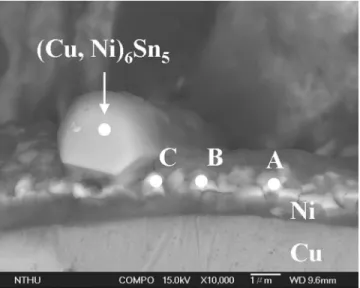
To investigate the phase transformation during the first and the third cycle of reflow, the composi-tions in the (Ni1–x,Cux)3Sn4 IMC near the (Cu1–y,
Niy)6Sn5 IMC were further investigated. Figure 5
shows the interfacial microstructure between the Sn-Pb solder/1-m Ni after three reflows. In this fig-ure, three trace points, i.e., one far away from (Cu1–y,
Niy)6Sn5; another near (Cu1–y,Niy)6Sn5, and the
other very close to (Cu1–y,Niy)6Sn5, were denoted as
A, B, and C, respectively. After detailed quantitative analysis by EPMA, the compositions of point A, B, and C are listed in Table I. For the trace point far away from (Cu1–y,Niy)6Sn5, the compositions of (Ni1–x,
Cux)3Sn4were very close to that in the as-reflowed
case. However, with the trace position close to the (Cu1–y,Niy)6Sn5IMC, Cu contents in (Ni1–x,Cux)3Sn4
increased. This implies that the amount of Cu disso-lution in (Ni1–x,Cux)3Sn4increased.
The composition of (Cu1–y,Niy)6Sn5 was identical
in all joints. That is to say, the value of y in (Cu1–y,
Niy)6Sn5remains constant. However, the value of x
in (Ni1–x,Cux)3Sn4 is not fixed. As described
previ-ously, x varied from 0.14 to 0.35 in the case of 1-m Ni. In the cases of 3-m, 5-m, 6-m, and 9-m Ni, the values of x in (Ni1–x,Cux)3Sn4varied from 0.09 to
0.35, 0.07 to 0.35, 0.05 to 0.35, and 0.02 to 0.35, re-spectively, again after deliberative EPMA analysis. Variations of x might be related to IMCs phase transformation in the consideration of ternary Ni-Cu-Sn phase equilibrium. A further investigation concerning this aspect is currently under way and will be reported in a future paper.
As mentioned previously, Cu diffused through electroplated Ni and reacted with Ni along the pas-sage, and then reacted with Sn from the solder to form (Ni1–x,Cux)3Sn4 after one reflow. Thus, the
x value in (Ni1–x,Cux)3Sn4 corresponded to the
amount of diffused Cu. With the increasing thick-ness of Ni, the amount of Cu diffused should de-crease. During the third cycle of reflow, the diffused Cu might dissolve into (Ni1–x,Cux)3Sn4to form (Ni1–z,
Cuz)3Sn4, where z indicates the maximum solubility
of Cu in Ni3Sn4. After Ni3Sn4reached its maximum
solubility of Cu, the excess Cu continued to diffuse through (Ni1–z,Cuz)3Sn4 into the solder. The excess
Cu then reacted with Ni and Sn to form (Cu1–y,
Niy)6Sn5. It should be pointed out that the growth
of Ni3Sn4 was limited during reflow, as shown in
Figs. 2 and 4. Thus, Cu could dissolve and diffuse through Ni3Sn4 easier. However, this phenomenon
did not occur everywhere. In general, the (Cu1–y,
Niy)6Sn5 IMC was first observed near the edge of
solder joints.
Cu Diffusion through Ni
The presence of Cu in Ni3Sn4 implies that Cu
might diffuse through Ni and substitute for the Ni sites. The surface morphology of 3-m Ni analyzed with an atomic force microscope is shown in Fig. 6, which indicates that the electroplated Ni exhibits a columnar structure. The Cu could move through the column boundary to enhance its diffusivity. With in-creasing thickness of Ni, the pathway for Cu atoms diffusion was prolonged. As a result, the degree of Cu migration through Ni was retarded and, thus, the x value in (Ni1–x,Cux)3Sn4was decreased, as
ob-served in the EPMA result. A further study concern-ing the diffusion behavior of Cu in this joint assem-bly will be reported in the near future.
CONCLUSIONS
After one reflow, only one layer of (Ni1–x,Cux)3Sn4
was found between solders and electroplated Ni in joints of a 63Sn-37Pb/Ni /Cu /Ti /Si3N4/Si multilayer
structure. As the thickness of Ni increased, the val-ues of x in (Ni1–x,Cux)3Sn4 decreased. Both layered
(Ni1–x,Cux)3Sn4and island-type (Cu1–y,Niy)6Sn5were
found between solders and electroplated Ni in all joints after three or five reflow times. When the thickness of Ni increased, the quantity of (Cu1–y,
Niy)6Sn5decreased. However, with increasing reflow
times, the quantities of (Cu1–y,Niy)6Sn5 increased.
After several reflows, Cu first diffused through elec-troplated Ni and reacted with Ni and Sn to form (Ni1–x,Cux)3Sn4. The Ni3Sn4 would then reach its
maximum solubility of Cu. Eventually, the excess Cu and Ni further migrated into solders to form (Cu1–y,Niy)6Sn5.
ACKNOWLEDGEMENTS
The financial support from Taiwan Semiconduc-tor Manufacturing Company is acknowledged. Par-Table I. Compositions of Trace Points A, B, and C
in Figure 5 Composition (at.%) Position Sn Ni Cu A 57.5 36.4 6.1 B 57.1 34.0 8.9 C 56.9 27.9 15.2
Under-Bump Metallization and Eutectic Sn-Pb Solder in Flip-Chip Technology 93
a
d e
c b
Fig. 4. The cross-sectional images of solder/UBM interfaces after three reflow times: (a) 1-m Ni, (b) 3-m Ni, (c) 5-m Ni, (d) 6-m Ni, and (e) 9-m Ni.
94 Huang, Duh, Chen, and Wang
Fig. 5. The interfacial microstructure between Sn-Pb solder/1-m Ni after three reflow times. Point A: far away from (Cu,Ni)6Sn5; point B:
near (Cu,Ni)6Sn5; and point C: very close to (Cu,Ni)6Sn5.
Fig. 6. The surface morphology of as-deposited 3-m Ni film.
tial support from the National Science Council under Contract No. NSC-90-2216-E007-058 is also acknowledged.
REFERENCES
1. J.H. Lau, Flip Chip Technologies (New York: McGraw-Hill, 1996).
2. C.S. Chang, A. Oscilowski, and R.C. Bracken, IEEE Circ.
Dev. Mag. 14, 45 (1998).
3. D.S. Patterson, P. Eleniu, and J.A. Leal, Adv. Electron.
Packaging 1, 337 (1997).
4. A.A. Liu, H.K. Kim, K.N. Tu, and P.A. Totta, J. Appl. Phys. 80, 2774 (1996).
5. H.K. Kim, K.N. Tu, and P.A. Totta, Appl. Phys. Lett. 68, 2204 (1996).
6. D.R. Frear, F.M. Hosking, and P.T. Vianco, Materials
Devel-opments in Microelectronic Packaging Conf. Proc., ed.
P. Singh (Materials Park, OH: ASM International, 1991), pp. 229–239.
7. S. Bader, W. Gust, and H. Hieber, Acta Metall. Mater. 43, 329 (1995).
8. S.K. Kang, R.S. Raiand, and S. Purushothaman, J.
Elec-tron. Mater. 25, 1113 (1996).
9. C.E. Ho, Y.M. Chen, and C.R. Kao, J. Electron. Mater. 28, 1231 (1999).
10. P.G. Kim, J.W. Wang, T.Y. Lee, and K.N. Tu, J. Appl. Phys. 86, 6746 (1999).
11. T.M. Korhonen, P. Su, S.J. Hong, M.A. Korhonen, and C.Y. Li, J. Electron. Mater. 28, 1146 (1999).
12. J.I. Goldstein, Scanning Electron Microscopy and X-ray
Microanalysis (New York: Plenum Press, 1981).
13. B.L. Young and J.G. Duh, J. Electron. Mater. 30, 878 (2001).
14. G. Ghosh, Acta Mater. 48, 3719 (2000).
15. J.Y. Park, C.W. Yang, J.S. Ha, C.U. Kim, E.J. Kwon, S.B. Jung, and C.S. Kang, J. Electron. Mater. 30, 1165 (2001).