國 立 交 通 大 學
電子工程學系 電子研究所碩士班
碩 士 論 文
氟摻雜對應變矽於二氧化鉿堆疊式金氧半
場效電晶體其特性和可靠度的影響
Impact of Fluorine Incorporation on Characteristic
and Reliability Issues of the CESL Strained
nMOSFETs with HfO
2/SiON Gate Dielectric Stack
研 究 生:邱芳毓
Fang-Yu Chiu
指導教授:羅正忠 博士
Dr. Jen-Chung Lou
氟摻雜對應變矽於二氧化鉿堆疊式金氧半
場效電晶體其特性和可靠度的影響
Impact of Fluorine Incorporation on Characteristic and
Reliability Issues of the CESL Strained nMOSFETs with
HfO
2/SiON Gate Dielectric Stack
研 究 生:邱芳毓 Postgraduate:Fang-Yu Chiu
指導教授:羅正忠 博士 Dr. Jen-Chung Lou
國 立 交 通 大 學
電子工程學系 電子研究所碩士班
碩 士 論 文
A ThesisSubmitted to Department of Electronics Engineering & Institute of Electronics College of Electrical and Computer Engineering
National Chiao Tung University In Partial Fulfillment of the Requirements
For the Degree of Master In
Electronics Engineering July 2010
Hsinchu, Taiwan, Republic of China
中 華 民 國 九 十 九 年 七 月
氟摻雜對應變矽於二氧化鉿堆疊式金氧半
場效電晶體其特性和可靠度的影響
研究生:邱芳毓
指導教授: 羅正忠博士
國立交通大學 電子工程學系 電子研究所碩士班 摘要 根據2007年ITRS所訂定出的金氧半場效電晶體的閘極尺寸,當元件尺寸持 續縮小,因傳統的二氧化矽介電層,當厚度降到1至1.5奈米左右,會有顯著的量 子穿隧效應而導致漏電流大到無法忍受的規範。近年來使用高介電質材料來取代 二氧化矽介電層已被廣泛研究。相較於二氧化矽,在相同的等效厚度(EOT)之下, 高介電質物質有較厚的實際厚度,因此可以抵擋因量子穿遂效應而導致的大量漏 電。然而,以高介電質材料當閘極介電層卻遭遇到其它的問題要解決,如:介面
的粗糙度導致載子遷移率的下降;高介電質材料有較高的界面狀態產生及較多的 電荷捕捉,對臨限電壓的漂移有較嚴重的影響。
研究指出,材料間的應變作用,可讓遷移率上升,故驅動電流會有大幅度的 提升,對現今微縮的COMS元件來說,用應變作用導致遷移率上升,是非常重要 的突破,因為它不用增加額外的製程步驟卻可以提供更高的驅動電流,如:淺塹 渠絕緣(shallow trench isolation,STI),矽化反應(slicidation),接觸孔蝕刻停止層 (contact etch stop layer,CESL)等製程,皆可運用存在其應力施加於通道,使遷移 率上升。其中,接觸孔蝕刻停止層是最普遍使用於nMOSFET的方式。然而,以 電漿增強型化學氣相沉積(PECVD)沉積出的Si3N4氮化物薄膜,理想比並不佳, 其薄膜化學式更準確地可寫成SixNyHz,指出它為非理想比組成且其薄膜含有氫 (通常為9至30%)。其氫離子在後續製程中,會向下擴散至通道,使表面有大量的 Si-H鍵,這種較弱的鍵結,容易被熱載子打斷,造成元件在做熱載子應力的穩定 性不佳和可靠度劣化的問題。 本文提出在閘極介電層沉積前,使用離子佈值的方式使氟離子在後續的高溫 摻雜活化的過程中,使其擴散至通道和閘極介電層。我們發現,摻雜氟對於應變 矽元件的基本特性沒有顯著的降低,而分析可靠度方面,我們深入探討固定電壓 應力(CVS)和熱載子應力(HCS)效應下的影響。觀察到在應力的破壞下,有氟摻 雜的元件,有較小的臨界電壓偏移,對於元件的可靠度和穩定性都有明顯的改善。 其主要原因是來自於氟原子併入高介電閘極主體以及閘極層與通道界面間,不僅
可修補界面狀態的懸空鍵結(interface dangling bond)和較低界面狀態產生,且可 有效減少高介電閘極本體的捕捉電荷情形。 最後在應力測試後再進行回復(relaxation)的行為,在CVS下的回復行為, 觀察載子具有逃逸(de-trapping)特性,而有氟摻雜的元件有較少載子捕捉情形 (應力下)及較高逃逸能障使得有較少逃逸現象產生(回復下),這與先前討論 Frenkel-Poole傳導機制,有較深的載子捕捉位置有好的關連性。
Impact of Fluorine Incorporation on Characteristic and
Reliability Issues of the CESL Strained nMOSFETs with
HfO
2/SiON Gate Dielectric Stack
Student : Fang-Yu Chiu Advisor : Dr. Jen-Chung Lou
Department of Electronics Engineering & Institute of Electronics National Chiao Tung University
Abstract
From the scaling trend in ITRS 2007, the conventional SiO2 layer, which is only
1-1.5 nm thickness, would suffer serious leakage from tunneling effect. Therefore, the High-K dielectric layer is used to replace SiO2 dielectric layer.
We could apply its predominance to avoid its serious tunneling leakage current from quantum tunneling effect under the same effective oxide thickness (EOT), because the High-K dielectric has thicker physical thickness. However, this replacement also faces some challenges to solve. Like, degraded channel mobility from interface roughness; more serious VTH shift from higher interface states
generations and more oxide bulk charges, etc.
As our known, we could enhance mobility for drive current by strain engineering. In fact, for nowadays scaling CMOS, it is essential for better mobility. It is a good technique to improve driving current without extra processes. The techniques like, shallow trench isolation (STI), slicidation, contact etch stop layer (CESL) all could insert strain into channel for better mobility. Most of all, the most widely used technology is CESL for nMOSFETs. However, it could face the setbacks from its uncontrollable quality Si3N4 deposited by PECVD. Since its variable composition
control, the layer is called SixNyHz precisely, which indicates its hydrogen content (9~30%). Worst of all, hydrogen would diffuse into the interface of dielectric layer and channel and then eventually result degraded reliability and uncontrollable characteristics。
In my thesis, we incorporate fluorine before gate dielectric deposition via channel implantation technique, which was subsequently diffused into the gate stack during annealing process. The implanted fluoride effect little for device characteristics degradation. For its reliability, we also analyze deeply its effect on constant voltage stress (CVS) and hot carrier stress (HCS). We found the device with fluoride dopants would suffer smaller VTH shift after stress. It is on of evidences fluoride advantage on
dopanted fluorine ions into the interface between interface of dielectric layer and channel would recovery interface dangling bonds result in lower interface state generations and eventually reduces High-K dielectric layer bulk trapping.
After CVS relaxation, with fluorinated device, less carrier are trapped after stress and less de-trapping from deeper traps barrier height after relax. This phenomenon could elucidate from Frenkel-Poole emission for relation between de-trapping and its traps location.
誌謝
考上交大後,很幸運的進到羅正忠老師的實驗室。在這兩年中,不論是在課業 及論文遇到的困難,老師及學長都會適時地給我幫助,讓我總是克服一次又一次 的問題,才能順利地拿到這個學位。由衷的感謝我的指導教授-羅正忠博士,不 但在論文的研究方向給予我很明確的指示,更教我們做人的道理和處事應對的態 度,讓我們日後出社會,不單是學到了專業知識,也學到了正確的學習態度,跟 倫理規範。 再者感謝,實驗室的博班學長-智仁與威良學長。特別要感謝智仁學長在實驗 及量測上給了我很多的幫助,每次量測看到不如預期的結果,多虧有智仁學長不 厭其煩的幫我看哪個環節出了問題,是儀器沒接好,還是條件設錯,或根本是元 件無法量測…等諸多原因,都會一一跟我細講是為什麼,慢慢的,自己也有了基 礎概念跟獨力解決問題的能力。真的是非常感謝智仁學長的教導。而威良學長算 是生活方面的益友,課業及論文上的幫忙當然是少不了,但在吃的方面,幫助更 大,每次實驗室的聚餐,沒有威良學長的吆喝,哪能成行!。然後很感謝實驗室 的奇葩-裳哥,在我們還是小碩一時,就很熱心的招待我們,過去的兩年訓練我 們機台,三不五時就請我們吃東西,論文實驗也是裳哥帶著做,這當中有許多的 酸甜苦辣,當下覺得很辛苦,有諸多的抱怨。但回過頭來想,這也是一種很特別 的人生體驗。當然,尚勳、文新,都是一起同甘共苦的好夥伴。沒有他們,我就 不能跟大家一起趴趴走,遠離只有二餐的日子!這份 ED523 的情誼,深刻印在我 心中。 當然不能忘記,我的男友小量和那些麻吉們(小逸、喬、錦屏、阿田、熊、逼), 給予我很多的鼓勵,每每聽我發發牢騷,當我的垃圾桶,對一開始很不習慣交大 生活的我,有人可以吐吐苦水。有這群夥伴相挺,才讓我有動力持續往前走。特 別感謝小量在口試前還撥空下來,幫我這個電腦白癡的報告做精美動畫,讓我沒 有後顧之憂。另外我在碩二的宿舍生活認識了兩個好室友-玉芬和佩砡,跟她們 一起住,真正享受到何謂宿舍生活,那些一起玩紙牌遊戲,瘋狂團購、打打鬧鬧 的日子,絕對是我第二年最美好的回憶,想到不能跟他們一起住,有無限感概啦! 最後要感謝的就是我的家人(充滿大道理的爸爸、超級辛苦的媽媽、酷酷的大 弟、可愛的Q明小弟),不論是發生甚麼事,好的壞的,回到家跟他們一起吃飯、 聊天,看電視…只是很普通的行為,就可以讓我煩惱,不順心的感覺都不再那麼 強烈,人可以很自然的放鬆,不禁大喊:有家的感覺真好!! 另外感謝我小弟, 考上隔壁校當我鄰居督促我這懶惰骨頭打羽球、慢跑,過著健康的生活,好像是 我的體能教練。(雖然宵夜也吃得多) 要感謝的人實在是太多,(栗子、文仙、張耀仁、蘇倉賢、張博翔…等)大家的 幫忙對我來說像一場又一場的及時雨,雖然無法一一列出所有的人和細節,只能 誠摯的向那些幫忙過我但未提及的人說一聲:謝謝!Contents
Abstract (Chinese)………...i
Abstract (English) ………...iv
Acknowledgement………vii
Contents………...viii
Table Captions………..……..x
Figure Captions………...………..……..…...xi
Chapter 1 Introduction
1.1 Introduction to High-K gate dielectric ... 1
1.1.1 Background ... 1
1.1.2 Recent High-K Gate Dielectric ... 4
1.1.3 Motivation ... 6
1.2 Introduction to CESL Induced Local Strained HfO
2nMOSFET. . 8
1.3 Organization of the Thesis ... 9
1.4 Reference ... 11
Chapter 2 Characteristic Issues of Fluorine Incorporation
on the CESL strained HfO
2/SiON gate dielectric
2.1 Introduction ... 18
2.2 Experimental Procedure ... 19
2.2.1 Device Fabrication Flow ... 19
2.2.2 Suitable Measurement Setup ... 21
2.3 Result and Discussions ... 22
2.3.2 Effect of various fluorine dose ... 26
2.3.3 Current Transport Mechinsm ... 27
2.4 Summary ... 30
2.5 References ... 30
Chapter 3 Reliability Issues of Fluorine Incorporation on the
CESL strained HfO
2/SiON gate dielectric
3.1 Reliability Review ... 48
3.2 Reliability Impact of Fluorine Incorporation on CVS ... 50
3.2.1 CVS Measurement Setup ... 50
3.2.2 Result and Discussions ... 50
3.3 Reliability Impact of Fluorine Incorporation on HCS ... 51
3.3.1 HCS Measurement Setup ... 51
3.3.2 Result and Discussions ... 52
3.4 The Characteristics of Charge De-trapping ... 53
3.5 Summary ... 55
3.6 References ... 56
Chapter 4 Conclusions and Future Works
4.1 Conclusions ... 65
4.2 Suggestions for Future Works ... 66
Table Captions
Chapter 1
Figure captions
Chapter 1
Fig. 1.1 Power dissipation (dynamic + static power) with each generation………….15 Fig. 1.2 Measured and simulated Ig-Vg characteristic under inversion conditions of
SiO2 nMOSFET device………15
Fig. 1.3 By using high-k material to suppress gate direct-tunneling current………...16 Fig. 1.4 FIBL causes increased off-state leakage in 1.5nm equivalent thickness high-K
gate dielectrics devices (more for the case of no oxide buffer)………16 Fig. 1.5 TEM and SIMS analysis of Y2O3 high-k dielectric with capped and uncapped
samples. Uncapped Y2O3 sample shows additional interfacial layer due to
oxygen diffusion………...17 Fig. 1.6 Schematic representation of factors contributing to carrier mobility
degradation in a high-k oxide layer………17
Chapter 2
Fig. 2.1 Fluorine incorporation via channel implantation………33 Fig. 2.2 The process flow of nMOSFETs with HfO2/SiON gate stack (a) control (b)
strained with and without SSFI………...34 Fig. 2.3(a) Schematic cross section of nMOSFETs with HfO2/SiON gate stack…….34
Fig. 2.3(b) Schematic cross section of CESL nMOSFETs with HfO2/SiON gate stack
with and without fluorinated………..35 Fig. 2.4 The experimental setup for the basic electrical characteristics and long-term
reliability test measurements………...35 Fig. 2.5 SIMS depth profile of the HfO2/SiON gate dielectrics. Fluorine atoms
Fig. 2.6 The X-ray Photon electron Spectroscopy (XPS) analysis of the F 1s
electronic spectra of SSFT treatment samples………...36 Fig. 2.7 Hf 4f Electron Spectra Chemical Analysis (ESCA) of (a) without fluorinated and (b) fluorinated, respectively……….37 Fig. 2.8 The ID-VG and Gm-VG (normalized VG) characteristic of the control
nMOSFET and the strained nMOSFET with and without fluorine………...37 Fig.2.9 The ID-VD output characteristic curves of the control nMOSFET and the
strained nMOSFET with and without fluorine……….38 Fig. 2.10 Gate leakage current as a function of gate voltages of the control nMOSFET
and the strained nMOSFET with and without fluorine. Both under inversion and accumulation regions……….38 Fig. 2.11 The C-V characteristics of HfO2 gate dielectrics with various fluorine doses.
………..39 Fig. 2.12 The maximum transconductance versus channel length for all splits of
HfO2/SiON gate stack nMOSFETs………..39
Fig. 2.13 The ID-VG transfer and Gm-VG characteristic of the CESL strained devices
with fluorine doses are 1E12cm-2, 1E13cm-2, 1E14cm-2, respectively……40 Fig. 2.14 The ID-VD output characteristic of the CESL strained devices with fluorine
doses are 1E12cm-2, 1E13cm-2, 1E14cm-2, respectively………..40 Fig. 2.15 Gate leakage current as a function of gate voltages with various fluorine
doses……….41 Fig. 2.16 Gate leakage current versus gate bias for fresh n-channel devices at different
temperatures (a) TEOS P.L (b) SiN P.L (c) SiN P.L with SSFI…………..43 Fig. 2.17 Conduction mechanism for source/drain current fitting under inversion
(a) TEOS P.L (b) SiN P.L (c) SiN P.L with SSFI………..46 Fig. 2.19 Band diagrams for (a) TEOS P.L (b) SiN P.L (c) SiN P.L with SSFI
illustrating the conduction mechanism of Frenkel-Poole emission…………47
Chapter 3
Fig. 3.1 Schematic of measurement setup for CVS measurement………...59 Fig. 3.2 CVS-stress-time dependence of ΔVth for Control, SiN capping and SiN
capping with SSFI at 25°C……….59 Fig. 3.3 The normalized gate current density ((Jg-Jg0)/Jg0) at a constant gate voltage of 4.0V versus stress time of all splits………60 Fig. 3.4 Schematic of measurement setup for HCS measurement………...60 Fig.3.5 Substrate current versus gate voltage for these samples of HfO2/SiON gate
stack n-MOSFETs………...61 Fig. 3.6 Threshold voltage shift as a function of stress time with HCS which compares
control, SiN CESL and SSFI+SiN CESL………...61 Fig. 3.7 The fluorinated CESL device has a large amount of F atoms incorporating to
passivate the bulk and interface trap charges of HfO2/SiON gate stack n-MOSFET……….62 Fig. 3.8 Threshold voltage shift with de-trapping bias -2V dependence after positive
voltage stress on these samples………..62 Fig. 3.9 The time-to-breakdown (TBD) characteristic of the nMOSETs with TEOS
P.L, SiN P.L and fluorinated SiN P.L………63 Fig. 3.10 On current degradation of the nMOSETs with TEOS P.L, SiN P.L and
fluorinated SiN P.L………..63 Fig. 3.11 Schematic of reliability improvement for the fluorine incorporation……...64
Chapter 1 Introduction
1.1 Introduction to High-K gate dielectric
1.1.1 Background
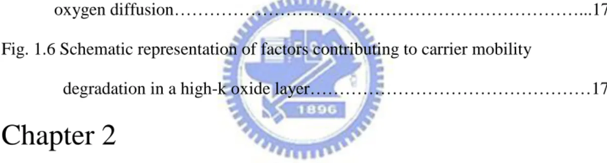
With IC technology flourish, the Moore’s Law, proposed by Gordon Moore in 1965, states that the number of transistors on integrated circuits doubles every 18 months. The key factor for Moore’s Law being obeyed is that Wafer Fabrication can continuously introduce new manufacturing techniques, so as to decrease feature size and minimize critical dimension (CD). Therefore, they can increase the number of transistors on the chip on time. Scaling raises chip speed and promote performance; increasing the number of transistors costs down making chips[1-2]. Thinner gate oxide provide higher drive current and improve gate control to channel so that suppress short channel effect (SCE) [3-4]. According to the 2007 ITRS (International Technology Roadmap for Semiconductors) roadmap, the SiO2 gate dielectric film
thickness should be scaled down to 1.0 nm for 35nm technology node (Table 1.1)[7]. However an ultra-thin SiO2 film comprising a few atomic layers causes a certainly large direct-tunneling current through the film. The direct tunneling current which depends on physical film thickness (Tph) (equation1.1) could cause an intolerable
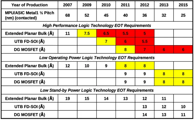
Where A is the fraction of gate actively switching and C is the total capacitance
load of all gate. The sum of dynamic power component (ACV2f) and static power component (VIpeak) defines total power consumption. Gate oxide continues shrinking,
static power consumption will increase due to gate oxide leakage and subthreshold leakage current (Fig.1.1). In addition, reliability issues become a serious concern for a thin SiO2 dielectric only 1-1.5nm. It points out that SiO2 uniformity is even more
difficulty in the growth of such a thin film, since even a mono-layer difference in thickness represents a large percentage difference and thus can result in the variation of threshold voltage (Vth) across the wafer. As shown in Fig. 1.2, we can see that
when the gate oxide thickness scales down to 2nm, the leakage current will exceed the limit of 1A/cm2 set by the allowable stand-by power dissipation. Further scaling of oxide thickness to below 2 nm, the direct tunneling current will increase exponentially, causing intolerable power consumption.
To reduce the tunneling leakage current, the new materials High-k dielectric has been widely investigated as possible replacement to the SiO2 film as gate insulators
[5-6]. According to the first order current-voltage relation in equation (1.3), the driving current of a MOSFET can be given as
Where VGS is the applied gate to source voltage, L is the effective channel length,
W is the channel width, VTH is the threshold voltage, is the electron mobility, Cox is
the gate capacitance, k is the dielectric constant, is the permittivity of free space and Tox is the oxide film thickness.
In order to improve the current drivability, we can reduce threshold voltage, increase operation voltage, shorter channel length and bigger capacitance or mobility. However, some methods have their limitations. A larger VGS will cause the reliability
issue. VTh is too small to result in statistical fluctuation in thermal energy at typical
operation conditions of up to 100 °C. Hence a shorter L and bigger Cox (means reduce
oxide thickness equation (1.4)) will be useful to provide device performance. However, thinner oxide thickness could cause intolerable leakage current. To reduce the tunneling leakage current, the new materials High-k dielectric has been widely investigated that it replaced SiO2 dielectric. In order to maintain the same C value, C
can be written as follows: (equation (1.5))
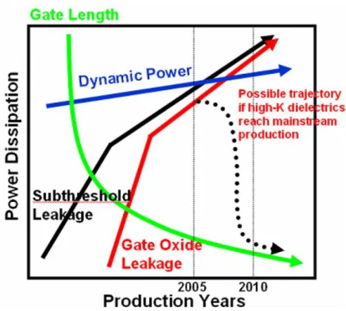
The main reason is that base on the same equivalent oxide thickness (EOT), high-K dielectrics have thicker physical film thickness, so it can significantly reduce
direct tunneling leakage current generating without sacrificing the performance, as shown in Fig. 1.3
Otherwise, the reliability issues become a huge concern for this thin regime of SiO2 film because the direct tunneling electrons make it more vulnerable for given
conditions and eventually cause a possible threshold voltage fluctuation or even dielectric breakdowns of devices, which result in a malfunction or failure of device [8]. Therefore, searching a material with a high dielectric constant to replace SiO2 is urgently needed.
1.1.2 Recent High-K Gate Dielectric
There are some critical principles to select proper high-k dielectric material. The first one is that the k value should be as high as possible, but it shouldn’t be too high. Because it could degrade the electrical properties due to increase field induced barrier lowering (FIBL) (Fig. 1.4) (i.e. fringing field from the gate to the source/drain which degrade short channel effects of MOSFETs [9].) On the same token, the k value shouldn’t be too low, otherwise it will lose its main propose of substituting for high-k materials. Secondly, the band offset obstructs carriers injected from the gate or source into a dielectric film.Hence, higherband offset is required.
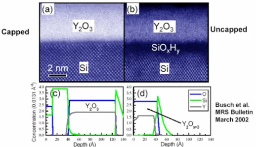
Si substrate are important. For all thin gate dielectrics, the interface with Si substrate plays a key role, and in most cases is the dominant factor in determining the overall electrical properties. Therefore, the high-k dielectrics require an interfacial reaction barrier to minimize the undesirable reactions with Si substrate. In addition, Fig. 1.5 shows the characteristics of oxygen diffusion through high-k dielectric materials [10]. Due to the rapid oxygen diffusion, an additional interfacial layer forms between the high-k dielectric and Si substrate. However, it is no benefit to scale down due to its low permittivity. Therefore, proper capping technology might be applied to avoid undesirable interfacial reaction with high-k dielectric.
Fourthly, Gate and fabrication process compatibility also are considered. The conventional poly gate with high-k dielectric does not seem to be a good technology any more. Because poly gate concerns poly depletion effect, it results in increase of EOT [11-12]. Otherwise,boron diffusion through high-k dielectric also degrades VTH
stability and reliability [12]. Moreover, Fermi level pinning affects narrow down of on-off margin in operation voltage of CMOS [13].
Various high-K dielectrics, including tantalum oxide (Ta2O5), yttrium oxide
(Y2O3), zirconium oxide (ZrO2), cerium oxide (CeO2), strontium titanate (SrTiO3),
and hafnium oxide (HfO2) have been extensively studied as the alternative gate
proper candidates under investigation, since its thermal stability in contact with silicon (47.6Kcal/mole at 727℃) compared to TiO2 and Ta2O5, high permittivity
(k~25~30 for HfO2) compared to Si3N4 and Al2O3, a large band gap 5.6eV with band
offsets to silicon >1.5eV, appropriate barrier high for both electrons and holes (> 1eV), and compatible with poly-silicon.
1.1.3 Motivation
There are still a number ofpending issues when high-k dielectrics are applied in future technology nodes, including high density of traps in the bulk dielectric and interfacial layer which will cause channel mobility degradation and threshold voltage instability. The high-k dielectric layer has soft optical phonons and the long-range dipole would degrade the effective carrier mobility in the inversion layer of the Si substrate [14]. Yang et al. [15] summarized the effects of all scattering and degradation mechanisms on the channel carrier mobility, as shown in Fig. 1.6.
The threshold voltage (VTH) shift of the poly-Si/high-k stack is another challenge
that must be considered. Reliability characteristics of the Hf-based dielectric such as hot carrier induced degradation (HCI), bias temperature instability (BTI), and time dependent dielectric breakdown (TDDB) have been investigated in the high-k dielectric gate stack. One of main issues for high-k gate stack is the charge trapping
characteristics during reliability test. Initial observation of instability was studied through capacitance-voltage (CV) characteristics in flat-band voltage change and current-voltage (IV) change.
Historically fluorine incorporation into gate dielectric is known as an effective way to passivate the interface traps in the conventional SiO2 gate dielectric and it can
improve device reliability because it was known that fluorine incorporation in the SiO2 gate dielectrics replaces Si–H bonds with Si–F bonds, Si-F bonds rather strong
than Si-H bonds. But the high-k oxides itself exist much more bulk defects than silicon oxide and suffer from a high density of charge traps. This causes instability of the gate threshold voltage, couloumbic scattering of carriers in the Si channel, and possible reliability problems. Recent research indicates that the main charge trap is the oxygen vacancy V0 [16]. F was found to substitute at the V0 site and passivates it.
In addition, the high-k oxides differ from Si:H or SiO2, i.e. they all have ionic
bonding, thus F is one of the best passivation for defects in an ionic oxide because it is the only element that is more electronegative than oxygen and its bond length is similar. Therefore fluorine incorporation was found to have a large beneficial effect on charge trapping [17-19] and can improve both the device performance and reliability.
known that excessive F annealing replaces Si–O bonds with Si–F bonds, which generates reactive oxygen atoms. The oxygen atoms react with silicon substrate and leading to form thick interfacial SiOx layer [20-21]. Therefore, the F ion concentration at the HfO2/SiO2 interface may be an essential aspect of such a defect
passivation scheme. Previous research suggests an insight into this problem. It was observed that the concentration of interstitial F ions was reduced by two orders of magnitude after a 400°C FGA. Hydrogen annealing seems to be able to remove excess F ions which are not strongly bonded in the bulk region of the HfO2 films [22].
1.2 Introduction to CESL Induced Local Strained HfO
2nMOSFET
As scaling of CMOS technology reaches its physical limitations, HfO2 gate
dielectric has received considerable attention due to advantages such as sufficiently high dielectric constant (15~25), good thermal stability, wide bandgap (5.6eV), and large band offset(~1.5eV)[23]. However, threshold voltage instability, low carrier mobility, and dielectric remain critical problems for High-K gate dielectric. The improvement of carrier mobility has also been intensely studied by introducing strain in the channel region. One of the most popular technologies is using high tensile-stress contact etch stop layer (CESL), which can obviously improve electron mobility and
drive current for nMOSFETs [24-26]. Therefore, a CESL strained high-K nMOSFET for high mobility application has been proposed. A high performance CESL strained nMOSFET with HfO2 dielectric is successfully demonstrated.
However, it could face the setbacks from its uncontrollable quality Si3N4 deposited
by PECVD. Since its variable composition control, the layer is called SixNyHz precisely, which indicates its hydrogen content (9~30%). Worst of all, hydrogen would diffuse into the interface of dielectric layer and channel and then eventually result degraded reliability and uncontrollable characteristics。Recent researches point out that at Si:SiO2 interfaces, the defect density is further lowered by hydrogenation, with any
Si dangling bond Pb scenters converted to Si–H bonds. Historically fluorine incorporation into gate dielectric is known as an effective way to passivate the interface traps in the conventional SiO2 gate dielectric and it can improve device reliability
because it was known that fluorine incorporation in the SiO2 gate dielectrics replaces
Si–H bonds with Si–F bonds, Si-F bonds rather strong than Si-H bonds. Therefore, for the first time, we try to do a novel CESL strained HfO2/SiON gate dielectric with
fluorinated to improve reliability problem.
1.3 Organization of the Thesis
fluorine incorporation into passivation dielectric of n-MOSFETs with HfO2/SiON
gate stack, evaluated in terms of reliability and performances. We study systematically the electrical characteristics of the CESL strained HfO2/SiON
dielectric with fluorinated, its reliability issues, and the behavior of charge trapping. In addition to this chapter that is dedicated to introduce the reason of the strained high-k dielectrics on CMOS technology and systematic discuss the effects of fluorine incorporating on MOSFETs with high-k gate dielectric stacks, this thesis is organized as follows :
In chapter 2, we describe the experimental procedure for fabricating n-MOSFETs test devices with HfO2/SiON gate stack as well as fluorine incorporation
dielectric. First, we use SIMS to analysis fluorine profile on interface between high-K dielectric and silicon substrate and use XPS to see whether fluorine can effectively bond with Hf. Then, show some basic electrical characteristics with and without fluorine incorporation, i.e., I-V and C-V characteristics.
In chapter 3 presents the effects of fluorine incorporation on HfO2 nMOSFET
reliability. Charge trapping characteristics, i.e., dynamic trapping analysis with stress dependent high-k film quality, threshold voltage shifts as indicating factors will be discussed. Besides, hot carrier reliability of the strained HfO2/SiON dielectric with
suggests that the high-k dielectric with fluorinated can provide optimistic results. In chapter 4, we conclude with summaries of the experimental results above and suggest the possible future researches in this area.
1.4 Reference
[1]
R. H. Dennard, F. H. Gaensslen, H. Yu, V. L. Rideout, E. Basson, and A. R. Lebanc,“Design of Ion-Implanted MOSFET’s with very small Physical Dimensions,” IEEE J. Solid State Circuits, SC-9, p.256, 1974.[2]
G. E. Moore, “Progress in Digital Intergrated Eletronics,” IEEE IEDM Tech. Dig., p.11, 1975.[3]
A. Hori and B. Mizuno, “CMOS device technology toward 50nm region performance and drain architecture”, IEDM Tech. Dig., p.641, 1999.[4]
B. E. Weir, P. J. Silverman, M. A. Alam, F. Baumann, D. Monroe, A. Ghetti, J.Bude, G. L. Timp, A. Hamad, and T. M. Oberdick, Tech. Dig. IEDM, p. 437 1999.[5]
M. Cao, P. V. Voorde, M. Cox, and W. Greene, IEEE Elec. Dev. Lett., 19, 291 1998.[6]
C-Y. Hu, D. L. Kencke, and S. Banerjee, “Determining effective dielectric thickness of MOS structures in accumulation mode”, Appl. Phys. Lett., 66 (13), p.1638 ,1995.[7]
The International Technology Roadmap for Semiconductor, Semiconductor Industry Association, San Francisco, CA, 2008.[8]
J. H. Stathis, “Physical and predictive models of ultra thin oxide reliability in CMOS devices and circuits”, IEEE Transactions on Device and MaterialsReliability, Vol. 1, pp. 43 -59, 2001.
[9]
G. C. F. Yeap, S. Krishnan, and M. R. Lin, “Fringing-induced barrier lowering (FIBL) in sub-100-nm MOSFETs with high-k gate dielectrics,” Electron. Lett., vol. 34, no. 11, pp. 1150–1152, 1998.[10]
B. W. Busch, O. Pluchery, Y. J. Chabal, D. A. Muller, R. L. Opila, J. Kwo, E. Garfunkel, “Materials Caracterization of Alternative Gate Dielectrics”,Materials Research Society Bulletin, 27, pp. 206-221, 2002.
[11]
Laegu Kang, Katsunori Onishi, Yongjoo Jeon, Byoung Hun Lee, Chang Seok Kang, Wen-jie Qi, Renee Nieh, Sundar Gopalan, Rino Choi, and Jack C. Lee, IEDM Tech. Dig., p. 35, 2000.[12]
K.Onishi, Laegu Kang, Rino Choi, E. Dharmarajan, S. Gopalan, Y.J. Jeon, Chang Seok Kang, Byoung Hun Lee, R. Nieh, and J. C. Lee, “Dopant Penetration Effects on Polysilicon Gate HfO2 MOSFET’s”, VLSI Tech. Dig., p.131 , 2001.[13]
Shiraishi K, Yamada K, Torii K, Akasaka Y, Nakajima K, Kohno M, et al. Physics in Fermi level pinning at the PolySi/Hf-based high-k oxide interface. Technical Digest International Symposium VLSI, 2004, p.108-9[14]
M.V. Fischetti, D.A. Neumayer, E.A. Cartier, J. Appl. Phys.90, 4587 , 2001.[15]
L. Yang, J.R. Watling, J.R. Barker, A. Asenov, in Physics of Semiconductors, vol. 27, ed. by J. Menedez, C.G. Van de Walle (AIP Press, 2005), p. 1497[16]
K. Xiong, J. Robertson, M. C. Gibson, and S. J. Clark, Appl. Phys. Lett. 87, 183505 2005.[17]
H. H. Tseng, P. J. Tobin, E. A. Herbert, S. Kalpat, M. E. Ramon, L. Fonseca, Z. X. Jiang, J. K. Schaeffer, R. I. Hegde, D. H. Triyoso, D.C. Gilmer, Tech. Dig. - Int. Electron Devices Meet. 2005, 713Yugami, J. Tsuchimoto, Y. Ohno, and M. Yoneda, Tech.Dig. - Int. Electron Devices Meet. 2005, 425.
[19]
K. I. Seo, R. Sreenivasan, P. C. McIntyre, and K. C. Saraswat, Tech. Dig. - Int. Electron Devices Meet. 2005,429.[20]
L. Tsetseris, X. J. Zhou, D. M. Fleetwood, R. D. Schrimpf, and S. T. Pantelides, “Dual role of fluorine at the Si−SiO2 interface,” Appl. Phys. Lett., vol. 85, no. 21, p. 4950, Nov. 2004.[21]
A. Kazor, C. Jeynes, and I. W. Boyd, “Fluorine enhanced oxidation of silicon at low temperatures,” Appl. Phys. Lett., vol. 65, no. 12,pp. 1572–1574, Sep. 1994.[22]
K. I. Seo, R. Sreenivasan, P. C. McIntyre, and K. C. Saraswat, Tech. Dig. - Int. Electron Devices Meet. 2005,429.[23]
L. Kang, Y. Jeon, K. Onishi, B.H. Lee, W.-J. Qi, R. Nieh, S.Gopalan, J.C. Lee, in: Symp. VLSI Tech. Dig., vols, 13–15, Honolulu, Hawaii, 2000, p. 44.[24]
C. T. Lin, Y. K. Fang, W. K. Yeh, C. M. Lai, C. H. Hsu, L. W. Cheng, and G. H. Ma, IEEE Electron Device Lett., vol. 28, pp. 376-378, 2007.[25]
S. Pidin, T. Mori, K. Inoue, S. Fukuta, N. Itoh, E. Mutoh, K. Ohkoshi, R. Nakamura, K. Kobayashi, K. Kawamura, T. Saiki, S. Fukuyama, S. Satoh, M. Kase, and K. Hashimoto, in IEDM Tech. Dig., pp. 213–216. 2004.[26]
T. Y. Lu, and T. S. Chao, IEEE Electron Device Lett., vol. 26, pp. 267-269, 2005.Table 1.1 2007 ITRS roadmap
*UTB FD-SOI : ultra-thin body fully-depleted silicon-on-insulator DG MOSFET : double-gate MOSFET.
: manufacturable solutions are NOT known.
13 15 9 9 8 10 8 6 5.5 7.5 40 2011 52 2009 11 13 14 DG MOSFET (Å ) 10 12 13 UTB FD-SOI (Å ) 11 12 14 19
Extended Planar Bulk (Å )
Low Stand-by Power Logic Technology EOT Requirements
8 8 9 DG MOSFET (Å ) 8 8 9 UTB FD-SOI (Å ) 8 9 12 Extended Planar Bulk (Å )
Low Operating Power Logic Technology EOT Requirements
6 6 7 DG MOSFET (Å ) 5.5 7 UTB FD-SOI (Å ) 5 6.5 11 Extended Planar Bulk (Å )
High Performance Logic Technology EOT Requirements
25 32
36 45
68 MPU/ASIC Metal1 ½ Pitch (nm) (contacted) 2015 2013 2012 2010 2007 Year of Production 13 15 9 9 8 10 8 6 5.5 7.5 40 2011 52 2009 11 13 14 DG MOSFET (Å ) 10 12 13 UTB FD-SOI (Å ) 11 12 14 19
Extended Planar Bulk (Å )
Low Stand-by Power Logic Technology EOT Requirements
8 8 9 DG MOSFET (Å ) 8 8 9 UTB FD-SOI (Å ) 8 9 12 Extended Planar Bulk (Å )
Low Operating Power Logic Technology EOT Requirements
6 6 7 DG MOSFET (Å ) 5.5 7 UTB FD-SOI (Å ) 5 6.5 11 Extended Planar Bulk (Å )
High Performance Logic Technology EOT Requirements
25 32
36 45
68 MPU/ASIC Metal1 ½ Pitch (nm) (contacted) 2015 2013 2012 2010 2007 Year of Production
Fig.1.1 Power dissipation (dynamic + static power) with each generation
Fig. 1.3 By using high-k material to suppress gate direct-tunneling current
Fig. 1.4 FIBL causes increased off-state leakage in 1.5nm equivalent thickness high-K gate dielectrics devices (more for the case of no oxide buffer)
Fig. 1.5 TEM and SIMS analysis of Y2O3 high-k dielectric with capped and uncapped
samples. Uncapped Y2O3 sample shows additional interfacial layer due to
oxygen diffusion.
Fig. 1.6 Schematic representation of factors contributing to carrier mobility degradation in a high-k oxide layer.
Chapter 2
Characteristics Issues of Fluorine Incorporation
on the CESL strained HfO
2/SiON gate dielectric
2.1 Introduction
There are still a number ofpending issues when high-k dielectrics are applied in future technology nodes, including high density of traps in the bulk dielectric and interfacial layer which will cause channel mobility degradation [1-2] and threshold voltage instability [3].In order to improve device performance, strain engineering has been proposed to increase carrier mobility for metal oxide semiconductor field transistors (MOSFETs) below to sub 90nm node [4-5]. In this situation, a nitride contact etch stop layer (CESL) is the most common strained method for nMOSFET. However, using plasma-enhanced CVD (PECVD) that deposits nitride strained layer has an undesirable problem of reliability degradation. Because gas source of PECVD is usually ammonia (NH3), in the follow-up process, hydrogen ions would downward
diffuse to gate dielectric layer and interface between dielectric layer and Si substrate and then formed Hf-H bond or Si-H bond, and both of which bonding energy are relatively weak. Therefore, when testing hot-carrier stress (HCS) reliability issues, it shows poorer consequence[6]. Previous studies demonstrated that for usual (no
bonding energy and enhance the electrical characteristics of high-k dielectric MOSFETs by eliminating inherent bulk traps[7-9]. In this work, we use silicon surface fluorine implantation (SSFI) method to attain role of fluorine passivation and then investigated the defect passivation with fluorine in a CESL strained nMOSFET with hafnium oxide (HfO2) and poly-Si gate. The novel fluorinated CESL gate stack
device obviously improves the gate dielectric/Si substrate interface immunity hot-carrier damage and exhibits better dielectric breakdown characteristic.
2.2 Experimental Procedure
The experiment propose a simple and effective fluorine incorporation technique that use SSFI method embedded in the CESL strained HfO2/SiON gate dielectric. In
the proposed fluorine incorporation method, we introduce the fluorine atoms into the HfO2 bulk material and the gate dielectric/Si substrate interface.
2.2.1 Device Fabrication Flow
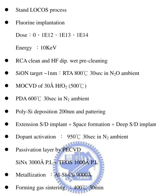
We use standard local oxidation of silicon (LOCOS) process for device isolation. The nMOSFET device was fabricated on 6-inch p-type (1 0 0) Silicon wafer. After forming 300Å sacrificial oxide, fluorine was incorporated by ion implantation. To investigate the effect of various fluorine concentrations on the device performances,
doses that we implanted are 1E12cm-2, 1E13cm-2 and 1E14cm-2, which defined as SSFI A, SSFI B, and SSFI C, respectively. The schematic diagram is shown in Fig. 2.1. After removing sacrificial oxide by dipping in HF solution, standard RCA clean was used to remove particles, organics and metal contamination. Immediately, a thin interfacial layer about 1nm oxynitride layer (SiON) was formed by a conventional rapid thermal oxide (RTO) at 800°C for 30sec in nitrous oxide (N2O) ambient. And
then 3nm HfO2 film was deposited by the AIXTRON metal organic chemical vapor
deposition system (MOCVD) at a substrate temperature of 500°C, followed by 600°C in nitrogen (N2) ambient RTA for 30sec in order to improve the quality of high-k
dielectrics. The physical thickness of the SiON and HfO2 films was measured by
optical N&K analyzer. Then a 200nm poly-silicon was deposited by low pressure chemical vapor deposition (LPCVD). Subsequently, gate electrode was defined by I-line lithography stepper and etched by ECR etching system. After removing sidewall spacer, S/D extension implantation was implemented by As implantation. Spacer formation was carried out by plasma-enhance chemical vapor deposition (PECVD) and then S/D implantation was executed by Arsenic implantation. After implanting, rapid thermal anneal (RTA) was performed at 950°C for 30sec in N2
ambient to activate dopant. Afterward, 3000Å-thick SiNx passivation layer was deposited by PECVD at 300°C with SiH4 and NH3. And then we deposited 1000Å
SiOx layer to avoid excessive stress. For comparison, the control sample was
deposited with a 4000Å -thick conventional PECVD-TEOS passivation layer. After passivation layer formation and contact hole pattering, Al-Si-Cu metallization was deposited by FSE-Cluster-Physical Vapor Deposition (PVD) system and then pattering. Finally, sintering process at 400°C for 30 minutes in N2 ambient is
eventually executed to finish our devices in this thesis.
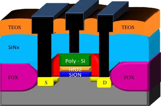
The main process flows are summarized in Fig. 2.2 (a) and (b). Schematic cross section of the control and strained HfO2/SiON n-MOSFETs with fluorine
incorporation is illustrated in Fig. 2.3(a) and Fig. 2.3(b), respectively.
2.2.2 Suitable Measurement Setup
The experimental setup for the I-V, C-V and reliability measurements of MOS device is illustrated in Fig. 2.4. Based on the PC controlled instrument environment, the complicated and long-term characterization procedures for analyzing the intrinsic and degradation behavior in MOSFET’s can be easily achieved.
Current-voltage (I-V) and capacitance-voltage (C-V) characteristics were evaluated by a HP4156A precision semiconductor parameter analyzer and an HP4284 LCR meter, respectively. The capacitance equivalent thickness (CET) of the gate dielectrics was obtained from high frequency (100KHz) capacitance-voltage (C-V)
curve at strong inversion without considering quantum effect.
To understand the content and distribution of the fluorine atoms was measured by secondary ion mass spectroscopy (SIMS), X-ray Photoelectron Spectroscopy (XPS) was used to analyze the Hf-O and Hf-F bondings of the fluorinated HfO2 thin films.
2.3 Result and Discussions
2.3.1 Effect of the strained device with and without
fluorine
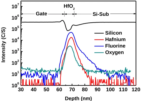
Fig. 2.5 shows the SIMS depth profile of the HfO2/SiON gate dielectric with
silicon surface fluorine implantation (SSFI) treatment. SIMS analysis is used to prove fluorine exist in HfO2/SiON dielectric, further in order to understand fluorine depth
profile. The experimental clearly result that fluorine atoms accumulated mainly at the interfacial layer. Therefore, we suggest that after fluorine implantation, the fluorine atoms would accumulate at the surface of the Si substrate, and then distributed into the bulk of HfO2 thin film after annealing. Besides, these fluorine atoms also
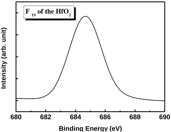
terminate the dangling bonds of silicon substrate and accumulate layer region [10] The X-ray Photon electron Spectroscopy (XPS) analysis of surface and bulk HfO2 thin films with SSFI treatment samples is shown in Fig. 2.7. XPS analysis is
traps due to the formation of Hf-F bonds. In Fig. 2.7, a distinct F 1s peak at 685eV can be observed. The silicon surface fluorine implantation process is obviously introducing fluorine atoms into the HfO2 dielectric to form the HfOF gate dielectrics.
Fig. 2.6 indicates the Hf 4f ESCA spectra of the HfO2/SiON dielectric with and
without fluorinated. We can observe that the fluorinated HfO2/SiON dielectric has
higher bonding energy, it proves that fluorine atoms would replace oxygen atoms to bond with hafnium atoms. Since fluorine atoms have the highest electronegativity, the Hf-F bonds could have much stronger bonding than Hf-O bonds. Therefore, Hf-F bonds could effectively immunity against damage.
Figure 2.8 shows the ID-VG at small drain voltage (VDS=100mV) transfer
characteristic of the control, the CESL and the CESL with SSFI (1E12cm-2) strained HfO2/SiON nMOSFETs, where the device channel length and width were 0.3 and
10µm, respectively. We can see that the CESL strained device has much higher drain current (ID) and transconductance (Gm), as well as smaller subthreshold swing (SS).
Comparing with conventional SiO2 passivation layer, the strained without and with
fluorinated gate dielectric can increase drain current and peak transconductance more than 100% and 115% , respectively. The subthreshold swing can be also improved from 108mv/dec to 97mv/dec and 96mv/dec to while instead SiO2 passivation layer
could significantly increase carrier mobility and indicate that has better interface characterization. Previous study [11] on Zr-silicate indicates that electron transport in the channel can be degraded by the coulomb scattering of negative charges in the bulk film, and Fischetti et. al [12] also points out that electron mobility in the inversion layer is affected by remote phonon scattering due to ionic polarization in high-k films. Therefore, the peak transconductance degradation in HfO2/SiON stack is probably
due to charges or traps in the bulk film. On the other hand, fluorine incorporation on the strained device does not degrade transfer characteristic, it still maintain good performance of the strained device. The results suggest that fluorine implantation will not bring bad effect to the strained gate dielectric.
The ID-VD output characteristic of the conventional, the CESL and the CESL
with SSFI (1E12cm-2) HfO2/SiON nMOSFETs are compared in Fig. 2.9 where the
device channel length and width were 0.3µm and 10µm, respectively. Approximate 39% drain current improvement measured at VG-VTh=1.5V is obtained for the strained
and the strain with fluorinated gate dielectric. The gate voltage has been normalized with respect to threshold voltage to minimize the effect of threshold voltage. And both of them (the strained with and without fluorinated) are not obviously different. The results also clearly suggest that the fluorinated CESL device does not degrade basic characteristic (transfer and output characteristic), it still maintain good performance of
the strained device. On the other hand, it clearly proves that strain process is beneficial to increase effective electron mobility which result in much higher saturation current. Fig. 2.10 displays the gate leakage current versus gate voltage (IG-VG) characteristic under inversion (positive sweep) and accumulation (negative
sweep) mode. Both the gate leakage current and breakdown voltage can be obviously improved by applying strain with and without fluorine incorporation process, which can be also ascribed to reduced interfacial and bulk trap densities.
The high-frequency (100kHz) C-V characteristic of the control, the CESL strained and the CESL with SSFI HfO2/SiON nMOSFETs are indicated in Fig 2.11
The extracted capacitance equivalent thickness (CET)is 3.79nm, 3.8nm and 3.77nm for the nMOSFETs with TEOS P.L, nitride P.L and nitride P.L with SSFI treatment, respectively, which were shown in the inset. Thickness of three is similar. It also means that fluorinated CESL device does not degrade basic characteristic. When fluorine concentration is higher than 1E12cm-2, the resultant CET increment faster may be an excess amount of fluorine incorporation into HfO2 film stacks. This is
related to the general theoretical results are the opposite. General theory tells us that implant more fluorine dose before depositing oxide, thickness is less. Otherwise, some researches point out that incorporation fluorine is after depositing oxide, fluorine atom has the highest electronegativity, the implanted fluorine atoms reveal
higher potential to replace the oxygen atoms. Consequently, the Hf-F bonds replace the Hf-O bonds then part of the residual oxygen would diffuse to the interface between HfO2/SiON stacked and Si substrate and react with the silicon dangling
bonds at the interface to growth low dielectric constant interfacial layer[14-17], which results in reduced capacitance and increased CET. Therefore, wet cant not find a rational to explain this result.
The relation between Gm and channel length for all splits of HfO2/SiON gate
stack n-MOSFET is shown in Fig. 2.12. When channel length becomes shorter, the improvement from strain process is more obvious because strain process must be playing in the small size that could exhibit its effect. In short, it was found that all fundamental electrical properties, including drive current, swing, gate leakage current, CET. These could obviously improvement by strain process and fluorine incorporation does not significantly affect these better performances.
2.3.2 Effect of various fluorine dose
Fig. 2.13 shows the ID-VG at small drain voltage (VDS=100mV) transfer
characteristic of the CESL strained devices with fluorine dose are 1E12cm-2, 1E13 cm-2, 1E14 cm-2, respectively. (where the device channel length and width were 0.3 and 10µm, respectively.) Unexpected, the improvement of the drain current,
transconductance and subthreshold swing do not change for the better with increasing fluorine doses. The subthreshold swing are 96mv/dec (1E12 cm-2), 98mv/dec (1E13 cm-2), 108mv/dec(1E14 cm-2), respectively. We can observe that when fluorine dose is 1E12 cm-2, the improvement effect is the best.
The ID-VD output characteristic of the the CESL strained HfO2/SiON
nMOSFETs devices with fluorine dose (1E12cm-2, 1E13cm-2, 1E14cm-2, respectively.) are compared in Fig. 2.14 where the device channel length and width were 0.3µm and 10µm, respectively. The experimental also shows the same result is that as fluorine dose more than 1E12 cm-2, the basic characteristic degrade with increasing fluorine. And Fig. 2.15 displays the gate leakage current versus gate voltage (IG-VG)
characteristic under inversion and accumulation mode. The result is not obviously different. We surmise that because redundant fluorine ions will band with hydrogen ions, resulting in worse performance. Therefore, the following discussion will not consider SSFI B and SSFI C due to their worse performance.
2.3.3 Current Transport Mechanism
Fig. 2.16 (a) and (b) and (c) show gate current IG as a function of VG for the
HfO2/SiON gate stacks with TEOS P.L, SiN P.L and fluorinated SiN P.L ,respectively.
accumulation regions. The current is temperature dependent that increases with increasing temperature. This implies that the conduction mechanism of gate current is trap-related, i.e., trap-assisted tunneling (TAT), Frenkel-Poole, etc. Base on the equation of Frenkel-Poole (F-P):
Where B is a constant in terms of the trapping density in the HfO2 film, ΨB is the
barrier height, Eox is the electric field in HfO2 film, is the free space permittivity,
is the HfO2 dielectric constant, KB is Boltzmann constant and T is the temperature
measured in Kelvin. Fig. 2.16 (a), (b) and (c) show the F-P plot for the source/drain current in inversion region for the control device and the strained without and with fluorinated, respectively. Fig. 2.17 (a), (b) and (c) show the F-P plot for the substrate current in inversion region for the control device and the strained without and with fluorinated, respectively. These lines are fitting curves for all temperatures. In the high voltage ISD and ISUB, an excellent linearity for each current characteristic can be
in nature.
The barrier height ΨB can be calculated from the intercept of y axis and the
dielectric constant of HfO2/SiON gate stacks can be determined by the slope of
the fitting curves according to Equation(2.3). On the other hand, the fitting parameters for the electron and hole barrier heights are 1.07eV and 1.36eV for the TEOS sample. The strained sample are1.2eV and 1.49eV, as compared to1.19eV and 1.5eV for the strained sample with fluorinated. Note that the barrier height for electrons has changed from 1.07eV for TEOS sample to 1.2eV for SiN sample and 1.19eV for strained SSFI sample, and for holes has changed from 1.36eV for TEOS to 1.49eV for SiN sample and 1.5eV for strained SSFI sample. This indicates that the trap position has moved closer to the conduction and valence band of the poly-si gate after strain process. The band diagrams are shown in Fig. 2.19 (a), (b) and (c) for the HfO2/SiON
gate stacks with TEOS P.L, SiN P.L and fluorinated SiN P.L, respectively. Because precursor of SiN sample is NH3, nitrogen atoms could recover shallow traps. SiN
samples with SSFI have fluorine atoms and it could recover shallow traps, similarly. Therefore both of them have deeper trap level than TEOS P.L. We consider the case when the injected carriers flow across HfO2/SiON by hopping via the trap sites with
energy barrier ΨB whose value depends on the fabrication process [4].This
with and without SSFI can be deeper than the TEOS sample, and the energy barrier ΨB for electrons is clearly lower than that for holes about 0.3eV in these samples.
2.4 Summary
In this chapter, a novel CESL strained high-k dielectric with implantation fluorine was presented. We have performed a systematical investigation of electrical characteristics. Significant device performance improvement in strained devices with and without fluorinated were found, such as the excellent subthreshold swing, increased transconductance, higher current drive, improved channel electron mobility, as compared to the control TEOS sample. These results suggest us that optimize fluorine incorporation (1E12cm-2) does not degrade basic electrical characteristic from strained effect. However, too much fluorine ions will degrade performance because of fluorine ions bending with because hydrogen ions.
Finally, the control device and the strained without and with fluorinated devices exhibit the F-P conduction mechanism for the gate leakage current in nature.
2.5 References
[1]
H. J. Cho, C. Y. Kang, C. S. Kang, R. Choi, Y. H. Kim, M. S. Akbar, C. H. Choi, S. J. Rhee, and J. C. Lee, “The effects of nitrogen in HfO/sub 2/ for improved MOSFET performance”, IEEE semiconductor Device Research Symposium.[2]
S. Zafar, A. Callegari, E. Gusev, and M. V. Fischetti, “Charge trapping related threshold voltage instabilities in high permittivity gate dielectric stacks, “ J. Appl. Phys. Vol. 93, pp.9298, 2003[3]
E. Gusev, D. A. Buchanan, and E. Cartier, “Ultrathin high-K gate stacks for advanced CMOS devices”, IEDM Tech. Dig., pp451,2001[4]
M. D. Giles, et al., “Understanding stress enhanced performance in Intel 90nm CMOS technology,” VLSI Symp. Tech. Dig., 2004, pp. 118-119.[5]
K. Mistry, et al., “Delaying forever: Uniaxial strained silicon transistors in a 90nm CMOS technology,” VLSI Symp. Tech. Dig., 2004, pp. 50-51[6]
K. T. Lee, et al., “A compressive study of reliability and performance of strain engineering using CESL stressor and mechanical strain,” IRPS Symp., 2008, pp. 306-309[7]
H.-H. Tseng, P. J. Tobin, E. A. Hebert, S. Kalpat, M. E. Ramon, L.Fonseca, Z. X. Jiang, J. K. Schaeffer, R. I. Hedge, D. H. Triyso, C.C. Capasso, O. Adetutu, D. Sing, J. Conner, E. Luckowski, B.W.Chan, A. Haggag, S. Backer, R. Noble, M. Jahanbani, Y. H. Chiu,and B. E. White, “Defect passivation with fluorine in aTaxCy/high- gate stack for enhanced device threshold voltage stability and performance,” in IEDM Tech. Dig., 2005, pp.696–699.[8]
M. Inoue, S. Tsujikawa, M. Mizutani, K. Nomura, T. Hayashi, K.Shiga, J. Yugami, J. Tsuchimoto, Y. Ohno, and M. Yoneda,“ Fluorine incorporation into HfSiON dielectric for Vth control and its impact on reliability for Poly-Si Gate pFET,” in IEDM Tech. Dig.,2005, pp. 413–416.[9]
K.-I. Seo, R. Sreeenivasan, P. C.McIntyre, and K. C. Saraswat,“ Improvement in high- (HfO2/SiO2) reliability by incorporation of fluorine,” in IEDM Tech. Dig.,pp. 2307-2310, 2005.
[11]
T. Yamaguchi, H. Satake, N. Fukushima, “Degradation of current drivability by the increase of Zr concentrations in Zr-silicate MISFET,” IEDM Technical Digest, 2001, p.663[12]
M. V. Fischetti, D. A. Neumayer, and E. A. Catier, “Effective electron mobility in Si inversion layers in metal-oxide-semiconductor systems with a high-k insulator: The role of remote phonon scattering,” J. Appl. Phys., vol.90,p.4587,2001[13]
T. Yamaguchi, H. Satake, N. Fukushima, and A. Toriumi, “Band Diagram and Carrier Conduction Mechanism in ZrO2/Zr-silicate/Si MIS Structure Fabricated by Pulsed-laser-ablation Deposition, “IEDM Tech. Dig., pp. 19-22, 2000.[14]
L. Tsetseris, X. J. Zhou, D. M. Fleetwood, R. D. Schrimpf, andS. T. Pantelides, “Dual role of fluorine at the Si−SiO2 interface ”Appl. Phys. Lett., vol. 85, no. 21, p. 4950, Nov. 2004.[15]
A. Kazor, C. Jeynes, and I. W. Boyd, “Fluorine enhanced oxidation of silicon at low temperatures,” Appl. Phys. Lett., vol. 65, no. 12,pp. 1572–1574, Sep. 1994[16]
H. Miyajima, R. Katsumata, Y. Nakasaki, Y. Nishiyama, and N. Hayasaka: Jpn. J. Appl. Phys. 35 (1996) 6217.[17]
W. J. Chang, M. P. Houng, and Y. H. Wang: Jpn. J. Appl. Phys. 38(1999) 4642.[18]
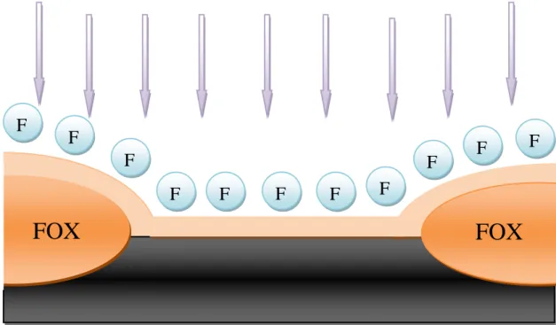
C. D. Young, et al., “Electron trap generation in high-k gate stacks by constant voltage stress,” Trans. Device Mater. Rel., vol. 6, No. 2, 2006, pp. 123-131.Fig. 2.1 Fluorine incorporation via channel implantation Stand LOCOS process
RCA clean and HF dip. wet pre-cleaning
SiON target ~1nm:RTA 800℃ 30sec in N2O ambient
MOCVD of 30Å HfO2 (500℃)
PDA 600℃ 30sec in N2 ambient
Poly-Si deposition 200nm and pattering
Extension S/D implant + Space formation + Deep S/D implant Dopant activation : 950℃ 30sec in N2 ambient
Passivation layer by PECVD Control : TEOS 4000Å P.L Metallization :Al-Si-Cu 9000Å Forming gas sintering :400℃ 30min
F
F
F
F
F
F
F
F
F
F
F
FOX
FOX
Stand LOCOS process Fluorine implantation
Dose:0、1E12、1E13、1E14 Energy :10KeV
RCA clean and HF dip. wet pre-cleaning
SiON target ~1nm:RTA 800℃ 30sec in N2O ambient
MOCVD of 30Å HfO2 (500℃)
PDA 600℃ 30sec in N2 ambient
Poly-Si deposition 200nm and pattering
Extension S/D implant + Space formation + Deep S/D implant Dopant activation : 950℃ 30sec in N2 ambient
Passivation layer by PECVD
SiNx 3000Å P.L + TEOS 1000Å P.L Metallization :Al-Si-Cu 9000Å Forming gas sintering :400℃ 30min
Fig. 2.2 The process flow of nMOSFETs with HfO2/SiON gate stack (a) control (b)
strained with and without SSFI
Fig. 2.3(b) Schematic cross section of CESL nMOSFETs with HfO2/SiON gate stack
with and without fluorinated
Fig. 2.4 The experimental setup for the basic electrical characteristics and long-term FOX
FOX
S D
30
40
50
60
70
80
90
100 110 120
10
010
110
210
310
410
510
610
7Silicon
Hafnium
Fluorine
Oxygen
In
te
n
s
it
y
(
C
/S
)
Depth (nm)
Gate
HfO
2Si-Sub
Fig. 2.5 SIMS depth profile of the HfO2/SiON gate dielectrics. Fluorine atoms
accumulated mainly at near the HfO2/silicon substrate interface after silicon
surface fluorine implantation (SSFI).
21 20 19 18 17 16 15 14 13 In te n si ty ( a r b . u n it ) (a) 16.14 16.66 21 20 19 18 17 16 15 14 13 (a) w/o Fluorinated
(b) Fluorinated
Hf
4f of the HfO2
Binding Energy (eV)
(b)
16.14
Fig. 2.6 The X-ray Photon electron Spectroscopy (XPS) analysis of the F 1s electronic spectra of SSFT treatment samples
680
682
684
686
688
690
F
1Sof the HfO
2In
te
n
s
it
y
(
a
rb
.
u
n
it
)
Binding Energy (eV)
Fig. 2.7 Hf 4f Electron Spectra Chemical Analysis (ESCA) of (a) without fluorinated and (b) fluorinated, respectively.
-0.6 -0.3
0.0
0.3
0.6
0.9
1.2
1.5
1.8
0
40
80
120
160
200
240
280
320
D
ra
in
c
u
rr
e
n
t
(m
A
)
Control
SSFI
SiN Capping
W/L=0.3/10
V
DS=0.1V
V
G-V
TH(V)
0
40
80
120
160
200
240
280
320
T
ra
n
s
c
o
n
d
a
n
c
e
(
S
)
0.0 0.5 1.0 1.5 2.0 2.5 3.0 0.0 0.2 0.4 0.6 0.8 1.0 1.2 1.4 1.6 1.8 2.0 D ra in C u rr e n t (m A ) Drain Voltage (V) W/L=0.3/10 Contorl SSFI SiN Capping VG-VTH=1.5V
Fig.2.9 The ID-VD output characteristic curves of the control nMOSFET and the
strained nMOSFET with and without fluorine.
-8 -6 -4 -2 0 2 4 6 8 10-14 10-13 10-12 10-11 10-10 10-9 10-8 10-7 10-6 10-5 10-4 10-3 10-2 L/W=2/10 Control SiN Capping SSFI G a te l e a k a g e c u rr e n t (A ) Gate Voltage (V)
Fig. 2.10 Gate leakage current as a function of gate voltages of the control nMOSFET and the strained nMOSFET with and without fluorine. Both under inversion and accumulation regions.
-2.0 -1.5 -1.0 -0.5 0.0 0.5 1.0 1.5 2.0 0.2 0.3 0.4 0.5 0.6 0.7 0.8 0.9 1.0
ControlNitride 1E12 1E13 1E14 3.2 3.3 3.4 3.5 3.6 3.7 3.8 3.9 4.0 4.1 4.2 CET( nm ) Control 1E12 1E13 1E14 Si3N4 Capping
C
ap
ac
it
an
ce
(
F
/c
m
2)
Applied Gate Voltage (V)
Fig. 2.11 The C-V characteristics of HfO2 gate dielectrics with various fluorine doses