國
立
交
通
大
學
電機學院 IC 設計產業研發碩士班
溝渠式橫向金氧半場效電晶體分析與最佳化設計之研究
Study on the analysis and optimization design of
Trench LDMOSFET
研 究 生:林宏春
Hung-Chun Lin
指導教授:羅正忠 博士
Dr.Jen-Chung Lou
溝渠式橫向金氧半場效電晶體分析與最佳化設計之研究
Study on the analysis and optimization design of Trench
LDMOSFET
研 究 生:林宏春
Student:Hung-Chun Lin
指導教授:羅正忠 博士
Advisor:Dr. Jen-Chung Lou
國 立 交 通 大 學
電機學院 IC 設計產業研發碩士班
碩 士 論 文
A Thesis
Submitted to College of Electrical and Computer Engineering National Chiao Tung University
in partial Fulfillment of the Requirements for the Degree of
Master in
Industrial Technology R & D Master Program on IC Design
January 2008
Hsinchu, Taiwan, Republic of China
溝渠式橫向金氧半場效電晶體分析與最佳
溝渠式橫向金氧半場效電晶體分析與最佳
溝渠式橫向金氧半場效電晶體分析與最佳
溝渠式橫向金氧半場效電晶體分析與最佳化設計之研究
化設計之研究
化設計之研究
化設計之研究
研究生:林宏春 指導教授:羅正忠 博士 國立交通大學電機學院產業研發碩士班摘要
摘要
摘要
摘要
隨著半導體產業的興起,高功率元件經常被應用在許多電力電子方面。功率 金氧半場效電晶體是功率元件其中一種,分別為橫向式與垂直式的結構。功率元 件為了與平面製程整合,必須設計成橫向式的結構,這就是橫向式金氧半場效電 晶體,它的特性是高的崩潰電壓與高的導通電阻。在本論文中,我們選擇溝渠式 橫向金氧半場效電晶體和使用模擬工具如ISE TCAD和MINITAB以減少面積和導通電 阻,以期待設計出150V的功率元件,並比較溝渠式橫向金氧半場效電晶體和橫向 金氧半場效電晶體間的效能。 最後,我們以電腦模擬得到在不同的情況下設定的崩潰電壓(300V)與導通電 阻,並且運用田口方法得到最佳化的設計。Study on the analysis and optimization design of
Trench LDMOSFET
Student:Hung-Chun Lin Advisor:Dr. Jen-Chung Lou
Industrial Technology R & D Master Program of
Electrical and Computer Engineering College
National Chiao Tung University
ABSTRACT
Power devices are widely applied to power electronics owing to great semiconductor industry. Power MOSFET is one kind of power devices, which has lateral and vertical structures. In order to integrate power MOSFET with planar IC process, this device must be designed the lateral structure, which is LDMOSFET. The characteristics of LDMOSFET are high breakdown voltage and high on-resistance. In this thesis, we choose Trench LDMOSFET and use simulation tools like ISE TCAD and MINITAB to reduce area and on-resistance, and look forward to design of 150V power device, and compare efficiency with LDMOSFET.
Finally, we use computer simulation to obtain the detail of breakdown voltage (300V) and on-resistance under different situations, and apply Taguchi Methods to gain optimal design.
誌謝
此篇論文之所以能順利完成,首先需感謝指導教授羅正忠博士平
日的細心指導,並且要感謝林柏村博士的支援與幫助。在這二年的學
習過程中,讓我學習到研究的態度及方法,也讓我的本職學能不斷的
累積與進步。
在研究所求學這段期間內,我特別要感謝523實驗室的所有人,因
為有大家的陪伴,讓我在研究所的日子留下美好的回憶。
最後,感謝我最親愛的家人,由其是要感謝妻子孟妙無怨無悔的
付出,因為她的支持和體諒,使我可以順利完成學業。小女佑真和未
出生的雙胞胎更是我甜蜜的助力。希望能以此論文的完成,獻給曾經
給我關心和幫助的人。
Contents
Abstract (Chinese)---I
Abstract (English)---II
Acknowledgment (Chinese)---III
Contents---IV
Table Captions---VI
Figure Captions---VII
Chapter 1 Introduction of Power MOSFET
1.1 General Background--- 1
1.2 Motivation---7
1.3 Organization of This Thesis---8
Chapter 2 Review of Principle
2.1 Structure and operation of LDMOSFET---9
2.2 Breakdown of LDMOSFET ---12
2.3 On-Resistance of LDMOSFET ---17
2.4 RESURF LDMOSFET ---20
Chapter 3 Analysis and Design of Trench LDMOSFET
3.1 Structure Analysis of LDMOSFET---24
3.2 Disadvantage of RESURF LDMOSFET---36
3.3 Advantage of Trench LDMOSFET---38
3.4 Design of Trench LDMOSFET---40
Chapter 4 Optimal design of Trench LDMOSFET
4.1 Introduction to experiment methods ---58
4.2 Procedure of Taguchi Methods---60
Chapter 5 Conclusions and Suggestions of Future Work
5.1 Conclusions---74
5.2 Suggestions of Future Work---75
Table Captions
Chapter3
Table 3.1 Process procedure of Trench LDMOSFET---45
Table 3.2 Parameter comparison of Power MOSFET---57
Chapter4
Table 4.1 Data of control factor and level---64
Table 4.2 Orthogonal Arrays for L
8(2
7)---65
Table 4.3 Interaction for L
8---66
Table 4.4 Data of simulation experiments---67
Table 4.5 Analysis of Variance table---68
Figure Captions
Chapter1
Figure 1.1 Applications for power semiconductor devices---5
Figure 1.2 The VMOSFET Structure---5
Figure 1.3 The DMOSFET Structure---6
Figure 1.4 The UMOSFET Structure---6
Chapter2
Figure 2.1 Conventional structure of DMOSFET---11
Figure 2.2 Structure of LDMOSFET---11
Figure 2.3 Reverse biased pn junction---14
Figure 2.4 Resistance of LDMOSFET---18
Figure 2.5 Potential distribution of LDMOSFET---19
Figure 2.6 Lateral RESURF structure full depletion---21
Figure 2.7 Electric field comparison at the surface---22
Chapter3
Figure 3.1 Structure of LDMOSFET---25
Figure 3.2 Breakdown voltage of cell pitch---26
Figure 3.3 On-resistance of cell pitch---26
Figure 3.4 Non-RESURF structure of LDMOSFET---28
Figure 3.5 RESURF structure of LDMOSFET---28
Figure 3.7 On-resistance of substrate concentration---29
Figure 3.8 Breakdown voltage of concentration of drift region---31
Figure 3.9 On-resistance of concentration of drift region---31
Figure 3.10 Breakdown voltage of epi depth---32
Figure 3.11 On-resistance of epi depth---32
Figure 3.12 Breakdown voltage of P-base concentration---34
Figure 3.13 On-resistance of P-base concentration---34
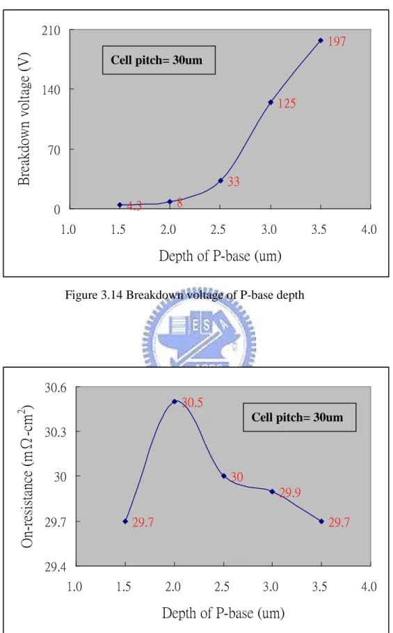
Figure 3.14 Breakdown voltage of P-base depth---35
Figure 3.15 On-resistance of P-base depth---35
Figure 3.16 Potential distribution of LDMOSFET (20um)---37
Figure 3.17 Electric field distribution of LDMOSFET (20um)---37
Figure 3.18 Structure of Trench LDMOSFET---38
Figure 3.19 Electric field of Trench LDMOSFET---39
Figure 3.20 Electric field of Trench LDMOSFET---40
Figure 3.21 Breakdown voltage of Trench LDMOSFET---42
Figure 3.22 Output Characteristics of Trench LDMOSFET---44
Figure 3.23 Process Flow Chart---46
Figure 3.24 Process Flow Chart---46
Figure 3.25 Process Flow Chart---46
Figure 3.26 Process Flow Chart---47
Figure 3.27 Process Flow Chart---47
Figure 3.28 Process Flow Chart---47
Figure 3.29 Process Flow Chart---48
Figure 3.30 Process Flow Chart---48
Figure 3.31 Process Flow Chart---49
Figure 3.33 Breakdown voltage of Trench depth---51
Figure 3.34 On-resistance of Trench depth---51
Figure 3.35 Structure parameter of Trench LDMOSFET---52
Figure 3.36 Breakdown voltage of L1 length---53
Figure 3.37 On-resistance of L1 length---53
Figure 3.38 Breakdown voltage of Polysilicon Gate length---55
Figure 3.39 On-resistance of Polysilicon Gate length---55
Chapter4
Figure 4.1 Breakdown voltage of original Trench LDMOSFET---61
Figure 4.2 On-resistance (Ron) of original Trench LDMOSFET---61
Figure 4.3 Format of
Cause and Effect Diagram---63
Figure 4.4 Analysis of
Cause and Effect Diagram---63
Figure 4.5 Linear Graph for L
8(2
7)---66
Figure 4.6 Response graph of control factor---70
Figure 4.7 Response graph of interaction ( Epi Con.*P-Base Con.)---71
Figure 4.8 Breakdown voltage of optimal Trench LDMOSFET---72
CHAPTER 1
Introduction of Power MOSFET
1.1General Background
The theory of Field Effect Transistor had been advent around 1920~1930 which is 20 years before the Bipolar Junction Transistor has been invented, which is from 1940’s and through early 1950s. At that time J.E. Lilienfeld of America suggested a transistor model having two metal contact at each side with metallic plate (Aluminum) on top of the semiconductor. The electric field at the semiconductor surface formed by the voltage supplied at the metallic plate enabled the control of the current flow between the metal contacts, and this was the initial conception of the Field Effect Transistor.But due to the immature semiconductor materials and the technology, the progress of the development was very sluggish. In 1952, W. Shockely introduced JFET (Junction Field Effect Transistors), in 1953, Dacey and Ross materiallized it. In JFET, the metallic plate of Lilienfeld structure was replaced by PN junction, and named the metal contact as source and drain, and also named the field effect electrode as gate. Even though there were continuous research of small-signal MOSFET after that, there was no prominent result for the power MOSFET, and the commercially available products started to come out by 1970s [1].
In the power MOSFET, the control signal is applied to a metal gate electrode that is separated from the semiconductor surface by an intervening insulator (typically
silicon dioxide). The control signal required is essentially a bias voltage with no significant steady-state gate current flow in either the on-state or the off-state. Even during the switching of the devices between these states, the gate current is small at typical operating frequencies because it serves only to charge and discharge the input gate capacitance. The high input impedance is a primary feature of the power MOSFET that greatly simplifies its gate drive circuitry.
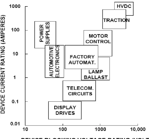
Power devices play a crucial role in the regulation and distribution of power and energy in the world. By some estimates, more than 60 percent of all the power utilized in the United States flows through at least one power device and more often through multiple devices. Consequently, the performance of power rectifiers and switches has a significant impact on the efficient use of electricity. In the power electronics community, it is well recognized that the improvements in system performance in terms of efficiency, size and weight are driven by enhancements made in semiconductor device characteristics. Some of the prominent applications for power semiconductor devices are shown in Figure 1.1, where the boxes indicate the device voltage and current ratings required to meet the system needs. It is obvious that the device ratings span a very broad range of voltages and currents. At relatively low voltages (< 100V), two important applications are in power supplies for computers, telecommunications or office equipment, and for automotive electronics. With the proliferation of personal computers, an improvement in the efficiency of the power supply is essential to reduce wastage of electricity. This will also lead to a reduction in the size and weight of the computer, which is attractive to consumers. The growth in power device applications in
automotive electronics is occurring due to the introduction of the multiplex bus architecture to replace point-by-point wiring in order to enhance manufacturability and reduce the weight of the wiring harness. Such a multiplex bus architecture can only be implemented by using smart power control at each of the large number of loads (lamps, motors, etc.) that are distributed throughout the car.
Due to its many attractive features, there has been a concerted effort to optimize its structure, design, and process technology. The development of discrete devices has followed the basic concept of the lateral channel structure and vertical channel structure. The lateral channel structure, all the drain, gate, and the source terminal are placed on the surface of a silicon wafer, and it is suitable for the integration but not for obtaining high power ratings as the length between the source region and the drain region must be far away from each other to obtain better voltage blocking capability, and as the drain-to-source current is inversely proportional to the length. The vertical channel structure, The drain and the source are placed in the opposite side of the wafer, and it is suitable for a power device as more space could be used as source region, and as the length between the source region and the drain region is reduced, it is possible to increase the drain-to-source current rating, and it could also increase voltage blocking capability by growing the epitaxial layer (drain drift region).
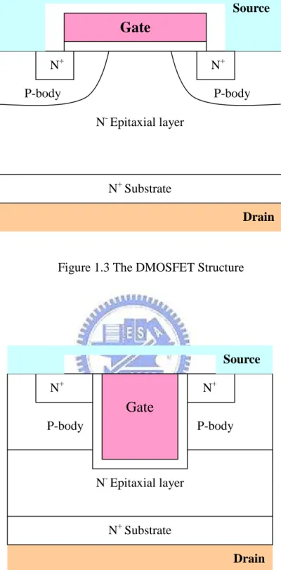
Three discrete vertical channel power MOSFET structures have been explored. The first structure was the vertical channel V-MOS power FET, shown in Figure 1.2, this structure has V-groove at the gate region and it is the first commercialized structure.
But as there was stability problem in manufacturing, and the high electric field at the tip of V-groove, this VMOSFET structure was pushed out by the DMOSFET structure. A cross-section of the DMOSFET structure is provided in Figure 1.3. This DMOSFET structure is fabricated by using planar diffusion technology with a refractory gate, such as polysilicon, as a mask. It has double-diffusion structure having P-base region and N+ source region, and it is the most commercially successful structure. The third power MOSFET structure, shown in Figure 1.4, this structure has U-groove at the gate region. This structure has higher channel density so that it can reduce on-resistance compared to the VMOSFET and the DMOSFET. UMOSFET structure using trench etching technique was commercialized in 1990s.
Figure 1.1 Applications for power semiconductor devices
Figure 1.2 The VMOSFET Structure
Drain N+ Substrate N- Epitaxial layer P-body P-body N+ N+
Gate
SourceFigure 1.3 The DMOSFET Structure
Figure 1.4 The UMOSFET Structure
Drain N+ Substrate N- Epitaxial layer P-body P-body N+ N+ Source
Gate
Drain N+ Substrate N- Epitaxial layer N+ SourceGate
P-body N+ P-body1.2 Motivation
In recent years, industries of LCD (Liquid Crystal Display) be progressed very quickly. When dots per inch (dpi), brightness and responding speed of LCDs are improved in every generation, the LCD driver IC must develop in the trend of high frequency and high voltage.
According to report of TSMC, Display technology is one of the fastest growing high voltage market segments. Flat panel displays, such as LCD displays, PDP and OLED displays, all use high voltage technology to produce driver ICs. The display compound annual growth rate (CAGR) over the next few years is 20-30%, with total revenues near $9 billion in driver IC consumption in 2006. The power management IC market is another fast growing segment. Power management devices provide power supplies and power devices for all electronics and are tied to the total electronic market growth. Analysts predict a CAGR of 15% for the next few years. Other popular applications, such as automotive and communication interface ICs and micro-mirror displays, require high voltage process technologies.
Applications of PICs (Power Integrated Circuits) are very popular in IT industry. Lateral power device is integrated into low-power circuits is current trend. In general, function of PICs request high efficiency, low cost, low consumption, small area. Therefore, using power device is Lateral DMOSFET, it is easy to integrated into plannar process, but conventional LDMOSFET has two disadvantage like high on-resistance and large area. In this thesis, we improve LDMOSFET to choose Trench
LDMOSFET, that is to say, drift layer of LDMOSFET adds to silicon dioxide of trench, it’s method to reduce on-resistance and area of device, and use the high voltage and low on-resistance property of Trench LDMOSFET to provide a high voltage device in LCD driver ICs. Power device simulator (ISE TCAD) [2] is used to simulate and evaluate the electrical and structural property of power device in order to get optimal process parameters.
1.3 Organization of This Thesis
This dissertation is divided into five chapters. The contents in each chapter are described as follows.
In chapter 1, the history of power MOSFET about conventional MOSFET、
VMOSFET、DMOSFET、UMOSFET devices are introduced in this chapter.
In chapter 2, this section focus on review of principle of LDMOSFET.
In chapter 3, this section focus on analysis and design of Trench LDMOSFET.
In chapter 4, and use Taguchi Methods to improve best efficiency of higher voltage and lower on-resistance of Trench LDMOSFET.
In chapter 5, this section includes the conclusions and the future work of this study.
CHAPTER 2
Review of Principle
Power MOSFETs in power integrated circuits, in the main, to do function of the switch. When the switch is off-state, power device come into being open circuit, which bear higher reverse voltage to avoid breakdown. Besides, the switch is on-state, power device come into being short circuit, which can help current pass through, moreover on-resistance is becoming more and more low. It is important to improve the power device performance by optimizing on-resistance for a given area and a breakdown voltage. A cost effective and elegant method to utilize such a trade-off between on-resistance and breakdown voltage is to optimize the device layout.
2.1 Structure and operation of LDMOSFET
Power MOSFETs have been widely applied to power electronics owing to great semiconductor industry, and have vertical channel and lateral channel structures. The power MOSFET in this thesis is LDMOSFET (Laterally Diffused MOSFET).What is LDMOSFET [3], in other words, this is lateral DMOS. In general, DMOS is a vertical structure, as shown in Figure 2.1. It is different to have Drain on the substrate of DMOSFET between DMOSFET and LDMOSFET. But Drain is on the surface of LDMOSFET, as shown in Figure 2.2.
and high blocking voltage. These features are obtained by creating a diffused p type channel region in a low-doped n type drain region. The low doping on the drain side results in a large depletion layer with high blocking voltage. The channel region diffusion can be defined with the same mask as the source region, resulting in a short channel with high current handling capability. The relatively deep p type diffusion causes a large radius of curvature at the edges, which eliminates the edge effects. While the device name implies that the fabrication require a diffusion, the dopants can just as well be implanted and annealed. Diffusion can be used in addition to further increase the junction depth and radius of curvature. The device can be fabricated by diffusion as well as ion implantation. The p type region is formed first, followed by shallow p+ and n+ regions. The n+ regions provide both source and drain contact regions. The p+ region contacts the p type body, which is typically shorted to the source, and eliminating the body effect.
It is the same to have operation principle of LDMOSFET and conventional MOSFET. For n channel LDMOSFET, positive voltage on the gate is increasing, and then electron in the P-base are attracted, and form a channel. Finally, the electron take shape a route, which include source, channel, drift layer and drain.
Figure 2.1 Conventional structure of DMOSFET
Figure 2.2 Structure of LDMOSFET N+ Substrate N-Drift Region N+ P-base Source Gate Drain PSubstrate N-Drift Region N+ P-base Source Gate Substrate N+ Drain
2.2 Breakdown of LDMOSFET
In power devices, large electric fields can occur both within the interior regions of the device where current transport takes place and at the edges of the devices. The voltage is supported across a depletion layer formed across either a PN junction, a metal semiconductor interface, or a metal oxide semiconductor interface. The electric field that exists across the depletion layer is responsible for sweeping out any holes or electrons that enter this region by the process of either space charge generation or by diffusion from the neighboring quasi-neutral regions. When voltage is increased, the electric field in the depletion region increases and the mobile carriers are accelerated to higher velocities. In the case of silicon, the mobile carriers attain a saturated drift velocity of about 1x107cm/sec. when the electric field becomes larger than 1x10⁵V/cm. In general, power devices cause breakdown which have 2 main kinds, Avalanche breakdown and Zener breakdown.
2.2.1 Avalanche Breakdown
Avalanche breakdown is caused by impact ionization of electron-hole pairs by carriers that have gained energy by accelerating in the high electric field in the depletion region of a reversed biased PN diode. The ionization rate is quantified by the ionization constants of electrons and holes,
α
n andα
p [4]. These ionization constants are defined as the change of carrier density with position divided by the carrier density or:M n
d =
α
Mdx ( 2.1 )The ionization causes a generation of additional electrons and holes. In order to compute the BV, it is necessary to determine the condition under which the impact ionization achieves an infinite rate. Generation of electron-hole pairs due to impact ionization requires a certain threshold energy (approximately 3.6eV for electrons and 5.0eV for holes in silicon) and the possibility of acceleration of the energy of electrons and holes, i.e. wide space charge regions. If the width of the space charge region is larger than the mean free path of carriers, charge multiplication occurs, which can cause electrical breakdown.
Consider a reverse-biased parallel-plane N+P junction with a positive bias applied to the N+ region (see Figure 2.3). Under the influence of the electric field E in the depletion region, the electron will be swept towards the N+ region and the hole will be swept towards the P region. Using the definitions for the ionization coefficients, the hole will create (αpdx) electron-hole pairs after traveling a distance (dx) and the
electron will create (αndx) electron-hole pairs. The total number of electron-hole pairs
M(x) created in the depletion region by a single electron-hole pair generated at a distance(x) is given by 0 ( ) 1 ( ) ( ) x W n p x M x = +
∫
α
M x dx+∫
α
M x dx ( 2.2 )Figure 2.3 Reverse biased pn junction
The integrations are performed along field lines through the depletion region. A solution of this integral equation is
(
)
(
)
0 0 exp ( ) 1 exp x n p W x p n p x dx M x dx dxα α
α
α α
− = − − ∫
∫
∫
( 2.3 )M(x) is commonly known as the multiplication coefficient. The breakdown voltage is defined as the voltage at which M(x) reaches infinity. It occurs if the
following integral equals one
(
)
0 exp 1 W x p n p x dx dxα
α α
− = ∫
∫
( 2.4 )The left-hand side of equation ( 2.4 ) is known as the ionization integral. With the approximation given in the avalanche breakdown condition corresponds to
0 1 W effdx
α
=∫
( 2.5 )The multiplication factor is commonly expressed as a function of the applied voltage and the breakdown voltage using the following empirical relation:
1 1 n M Va Vbr = − ( 2.6 )
Where n is in the range 2 to 6
Va is the applied (reverse) voltage Vbr is the breakdown voltage
2.2.2 Zener Breakdown
Zener breakdown occurs in heavily doped PN junctions. The heavy doping makes the depletion layer extremely thin. So thin, in fact, carriers can’t accelerate enough to cause impact ionization. With the depletion layer so thin, however, quantum mechanical tunneling through the layer occurs causing current to flow. The temperature coefficient of the Zener mechanism is negative breakdown voltage for a particular diode decreases with increasing temperature. However, the temperature coefficient is essentially independent of the rated breakdown voltage, and on the order of -3 mV/K [4].
In a Zener diode either or both breakdown mechanisms may be present. At low doping levels and higher voltages the avalanche mechanism dominates while at heavy doping levels and lower voltages the Zener mechanism dominates. At a certain doping level and around 6 V for Si, both mechanism are present with temperature coefficients that just cancel. It is possible to make Zener diodes with quite small temperature coefficients.
Neither Zener nor Avalanche breakdown are inherently destructive in that the crystal lattice is damaged. However, the heat generated by the large current flowing can cause damage, so either the current must be limited and/or adequate heat sinking must be supplied.
2.3 On-Resistance of LDMOSFET
Power devices in power integrated circuits, in the main, to do function of the switch. When the switch is on-state, and get lower on-resistance. Therefore, designing power devices need to know combination of on-resistance, and can get effective design and analysis. In structure of LDMOSFET, on-resistance is combined by three main resistance [1], which channel resistance (Rch), accumulation resistance (Ra) and drift region resistance (Rd). Thus on-resistance is as follows.
on ch a d
R =R +R +R ( 2.7 )
2.3.1 Channel Resistance
The definition of the LDMOSFET channel resistance is the same as that of the basic MOSFET. The contribution from the channel depend on the ratio (channel length/width), the gate oxide thickness (Cox), and the gate drive voltage (VG). To calculate the contribution from the channel, consider the resistance of LDMOSFET cell structure shown in Figure 2.4, The channel resistance (Rch) per cm2 for the linear cell structure is given by:
(
)
ch ch ns ox G T L R Wµ
C V V = − ( 2.8 )Where W is channel width Lch is channel length
µ
ns is electron mobility of channel surface Cox is gate oxide of capacitanceFigure 2.4 Resistance of LDMOSFET
2.3.2 Accumulation Layer Resistance
The resistance of the accumulation layer (Ra) accounts for the current spreading from the channel into JFET region. The accumulation layer resistance is dependent upon the charge in the accumulation layer and the mobility for free carriers at the accumulated surface. Thus, the inference of accumulation layer resistance is similar to channel resistance. The accumulation layer resistance per cm2 is:
(
A)
A nA ox G TA KL R Wµ
C V V = − ( 2.9 )Where LA is length of accumulation layer (from the edge of the P-base region to the right of the polysilicon gate (point A).
µ
nA is electron mobility of carrier accumulation of epitaxial layer surface. VTA is critical voltage of accumulation region.K is a proportionality constant. PSubstrate N-Drift Region N+ P-base Source Gate Substrate N+ Drain Rch RA RD
2.3.3 Drift Region Resistance
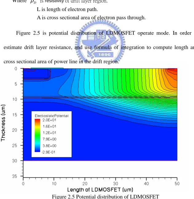
Drift region is in cell structure of LDMOSFET, and have a low concentration of epitaxial layer. We regard LDMOSFET as MOSFET plus a resistance, which is drift region resistance (RD). Therefore, the drift region resistance is estimated by formula of resistance. D L R A ρ = ( 2.10 )
Where
ρ
D is resistivity of drift layer region.L is length of electron path.
A is cross sectional area of electron pass through.
Figure 2.5 is potential distribution of LDMOSFET operate mode. In order to estimate drift layer resistance, and use formula of integration to compute length and cross sectional area of power line in the drift region.
2.4 RESURF LDMOSFET
High voltage devices usually require thick and low doped epitaxial layer, which makes them difficult to integrate with low voltage circuitry. Because of the high resistivity epitaxial layer, the on-state resistances of such devices is large. In 1979 Appels and Vaes suggested the reduced surface field (RESURF) concept [5]. The RESURF concept [6] gives the best trade-off between the breakdown voltage and the on-resistance of lateral devices. It has been shown that a lateral diode with a thin n type epitaxial layer on a lowly doped p substrate can give a higher breakdown voltage than a conventional lateral diode.
As shown in Figure 2.6 for a certain range of the n epitaxial (drift region) thickness and doping, the depletion region covers almost all the area of the thin epitaxial layer. It allows the depletion region to extend further than for the corresponding one-dimensional lateral diode without p substrate. As a result the surface field is decreased, and higher voltages can be applied to the devices. This is the well known RESURF effect. For an optimum doping and thickness of the n layer, a uniformly distributed voltage across the silicon surface in the drift region can be seen and a bulk breakdown voltage can be achieved. The breakdown voltage of lateral RESURF devices is limited by the substrate doping. The charge of the n layer determines the resistance of the drift region which is the most critical parameter of high-voltage devices. Together with the length of the drift region it will determine the on-resistance and current handling capability of the device.
Figure 2.6 Lateral RESURF structure full depletion
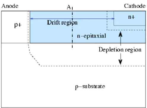
The RESURF technology has been one of the most frequently applied methods for the design of high-voltage lateral devices with low on-resistance [7,8,9]. It has been successfully used for lateral high-voltage devices such as diodes and LDMOS transistors for 20-1200V. This technology provides an efficient way to integrate high voltage devices with low voltage circuitry. The traditional RESURF structure is constructed by a lateral P+N diode (P+/N epitaxial) that defines the on-resistance characteristic of the device and a vertical P/N diode which supports a space charge depletion region enabling high BV (breakdown voltage).
The lateral BV of this structure depends on the N-epi net charge of the drift region, which is given when the N-epi net doping is integrated from the surface to the vertical PN junction (P substrate/N-epi) along the cut line A in Figure 2.6. Assuming that the N-epi layer is fully depleted with optimum drift dose, the maximum BV is determined
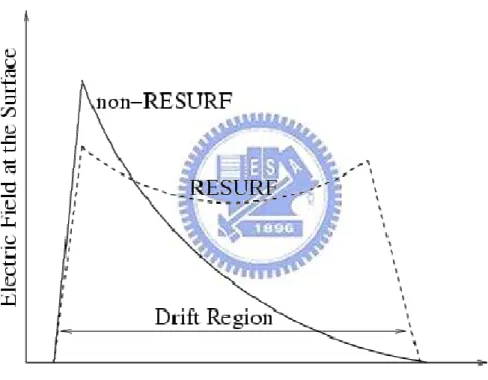
by the BV of the vertical PN diode (P substrate/N epitaxial). The drift region resistance is inversely proportional to the net charge in this region. Due to the vertical junction of the RESURF structure, a second electric field peak forms at the n+ cathode of the device. As shown in Figure 2.7 the electric field at the surface of the RESURF device (after full depletion) assumes a parabolic rather than a linear distribution which can be seen in conventional high voltage devices. It helps to reduce the electric field at the surface of the device during off-state.
Figure 2.7 Electric field comparison at the surface
The basic properties of RESURF structures are determined by the P substrate doping concentration (Csub), the N-epi layer doping concentration (N-epi), and the N-epi layer thickness (Tnepi). In the structure shown in Figure 2.6, an approximate net charge Qn of the N-epi layer (assuming uniform doping) is given by
n epi nepi
The BV performance depends significantly on the net charge Qn of the N-epi layer. The optimum Qn is found by assuming that the vertical depletion must reach the surface before the lateral junction breaks down. The vertical space charge width in the N-epi region extends and interacts with the lateral junction space charge region allowing the lateral depletion width to effectively span a larger distance compared to the case without the presence of the P substrate. As a result, the lateral electric field at the lateral P+N-epi junction is significantly reduced relative to the one-dimensional diode case, therefore enabling higher voltages to be applied. Consequently, to achieve a high BV in RESURF structures, it is required that the N-epi region is fully depleted before the lateral electric field reaches a critical value.
CHAPTER 3
Analysis and Dessssign of Trench LDMOSFET
In order to gain higher breakdown voltage of power MOSFET, conventional LDMOSFET is designed by needing to increase length of drift region. When length of drift region is getting longer, breakdown voltage and on-resistance are becoming larger. This is unfavorable factor. Thus, we use Trench LDMOSFET to improve the performance of LDMOSFET. The main object of this thesis is Trench LDMOSFET. The characteristic of the structure is to fill a SiO2 Trench in the drift region under the gate, which decrease on-resistance and increase breakdown voltage is better than conventional LDMOSFET. Gaining higher breakdown voltage and reducing area of device are anticipated by design of Trench LDMOSFET.
3.1 Structure Analysis of LDMOSFET
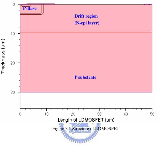
RESURF technology to gain high breakdown voltage, to change physical property, and decide to adopt one factor at a time, to observe electric property of cell pitch, substrate concentration, concentration and thickness of drift region, and concentration and thickness of P-base. Thus, the specification of LDMOSFET parameter include cell pitch (50um), P-substrate (1E14cm-3), concentration of drift region (4E14cm-3), depth of drift region (9um), concentration of P-base (1E15cm-3), depth of P-base (3um), and concentration of the source and drain (1E17cm-3) as shown in Figure 3.1.
Figure 3.1 Structure of LDMOSFET
3.1.1 Cell pitch
Cell pitch is getting large, and breakdown voltage is also higher, but cost must add, this method can not avoid. According to Figure 3.2 and Figure 3.3, length of LDMOSFET is becoming long, breakdown voltage and on-resistance are getting large at the same time.
P substrate Drift region (N-epi layer) P-Base
Figure 3.2 Breakdown voltage of cell pitch
Figure 3.3 On-resistance of cell pitch
39 125 136 153 195 0 50 100 150 200 250 10 20 30 40 50 60 70
Cell pitch (um)
B
re
ak
d
o
w
n
v
o
lt
ag
e
(V
)
12.6 29.9 42 56.3 68.7 0 10 20 30 40 50 60 70 80 10 20 30 40 50 60 70Cell pitch (um)
O
n
-r
es
is
ta
n
ce
(
m
Ω
-c
m
2)
3.1.2 Substrate Concentration
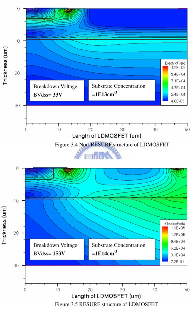
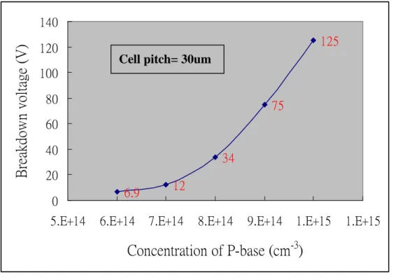
RESURF theorem can get up to effect of reducing surface electric field, and makes use of vertical full depletion region (P type substrate and N type drift region), the
junction takes place high electric field. When substrate concentration is smaller than critical concentration, drift region is not covered by upward depletion region, and can’t develop RESURF function. LDMOSFET under gate takes place breakdown because electric field of lateral depletion region of P-base and gate edge as shown in Figure 3.4. When substrate concentration is greater than critical concentration, drift region is covered by upward depletion region, and device has RESURF function. LDMOSFET under gate and drain takes place breakdown because electric field of lateral depletion region of P-base and gate edge as shown in Figure 3.5. When substrate increases concentration, the depletion region of PN junction is getting large, breakdown voltage is also raising as shown in Figure 3.6. and Figure 3.7. By the two figure, and use one factor at a time, to observe breakdown voltage is 179V, in other words, the substrate concentration is 5E14cm-3, and gain breakdown voltage. But change of substrate concentration will increase production cost. Therefore, substrate concentration of Trench design is still 1E14cm-3, and this device has effect of junction isolation, to turn on-state, drain current don’t pass through substrate, substrate resistance is ignored that affects on-resistance.
Figure 3.4 Non-RESURF structure of LDMOSFET
Figure 3.5 RESURF structure of LDMOSFET Breakdown Voltage BVdss= 33V Substrate Concentration =1E13cm-3 Breakdown Voltage BVdss= 153V Substrate Concentration =1E14cm-3
`
Figure 3.6 Breakdown voltage of substrate concentration
Figure 3.7 On-resistance of substrate concentration
30 58 125 179 166 149 0 50 100 150 200
1.E+12 1.E+13 1.E+14 1.E+15 1.E+16
Substrate concentration (cm
-3)
B
re
ak
d
o
w
n
v
o
lt
ag
e
(V
)
5E14Cell pitch= 30um
29.5 29.7 29.9 30.3 30.2 30.1 29.4 29.9 30.4
1.E+12 1.E+13 1.E+14 1.E+15 1.E+16
Substrate concentration (cm
-3)
O
n
-r
es
is
ta
n
ce
(
m
Ω
-c
m
2)
3.1.3 Concentration and Thickness of Drift Region
Width of depletion region has relations with concentration of drift region and substrate, substrate decides whether drift region is covered by upward depletion region. If drift region is high concentration, it makes depletion region is getting small, electric field is getting large, substrate upward depletion region can not generate effective depletion, and causes under gate to take place breakdown as shown in Figure 3.8. If drift region is low concentration, width of substrate upward depletion region become large, RESURF performance is also getting better, and reverse voltage can gain high breakdown voltage. But concentration of drift region controls drift resistance, and it is getting high concentration, resistance of drift region is becoming small as shown in Figure 3.9.
Thickness of drift region affects RESURF technology, if it is too thick, substrate upward depletion region can’t cover whole drift region, and maximum electric field is under gate, to take place breakdown. When it is getting thin, substrate upward depletion region and lateral depletion region of P-base generate function, and reduce surface electric field of P-base, which avoids breakdown under gate, but electric field under drain is becoming large, in any case, this drift region (N-epi layer) is too thin, it causes breakdown under drain as shown in Figure 3.10 and Figure 3.11.
Figure 3.8 Breakdown voltage of concentration of drift region
Figure 3.9 On-resistance of concentration of drift region
179 125 15 12 10 0 50 100 150 200
0.E+00 2.E+14 4.E+14 6.E+14 8.E+14 1.E+15 1.E+15
Concentration of drift region (cm
-3)
B
re
ak
d
o
w
n
v
o
lt
ag
e
(V
)
Cell pitch= 30um
58.3 29.9 20.5 15.9 13.1 0 10 20 30 40 50 60 70
0.E+00 2.E+14 4.E+14 6.E+14 8.E+14 1.E+15 1.E+15
Concentration of drift region (cm
-3)
O
n
-r
es
is
ta
n
ce
(
m
Ω
-c
m
2)
Figure 3.10 Breakdown voltage of epi depth
Figure 3.11 On-resistance of epi depth
125
51
34
17
175
0 50 100 150 200 7 8 9 10 11 12 13Epi depth (um)
b
re
ak
d
o
w
n
v
o
lt
ag
e
(V
)
Cell pitch= 30um
31.2 29.9 28.6 27.9 27.5 27 28 29 30 31 32 7 8 9 10 11 12 13
Epi depth (um)
O
n
-r
es
is
ta
n
ce
(
m
Ω
-c
m
3.1.4 Concentration and Thickness of P-base
In this power MOSFET, the P-base region and the N+ source regions are diffused through a common window defined by the edge of the polysilicon gate. The name for this device is derived from this double-diffusion process. The P-base region is driven-in deeper than the N+ source. The difference in the lateral diffusion between the P-base and N+ source regions defines the surface channel region.
When a positive drain voltage is now applied, it reverse biases the P-base/N-drift region junction. This junction supports the drain voltage by the extension of a depletion layer on both sides. Due to the higher doping level of the P-base region, the depletion layer extends primarily into the N-drift region. Its doping concentration, depth and width must be chosen in accordance with the criteria established for avalanche breakdown of PN junction. A higher drain blocking voltage capability requires a lower drift region doping and a larger depth and width.
When concentration of the P-base region is getting high, breakdown voltage is also becoming large, but change of on-resistance is unapparent. If depth of the P-base region is getting deep, breakdown voltage is also becoming large as shown in Figure 3.12 to Figure 3.15.
Figure 3.12 Breakdown voltage of P-base concentration
Figure 3.13 On-resistance of P-base concentration
6.9 12 34 75 125 0 20 40 60 80 100 120 140
5.E+14 6.E+14 7.E+14 8.E+14 9.E+14 1.E+15 1.E+15
Concentration of P-base (cm
-3)
B
re
ak
d
o
w
n
v
o
lt
ag
e
(V
)
Cell pitch= 30um
29.8 29.8 29.8 29.9 29.9 29.7 29.8 29.9 30.0
5.E+14 6.E+14 7.E+14 8.E+14 9.E+14 1.E+15 1.E+15
Concentration of P-base (cm
-3)
O
n
-r
es
is
ta
n
ce
(
m
Ω
-c
m
2)
Figure 3.14 Breakdown voltage of P-base depth
Figure 3.15 On-resistance of P-base depth
4.3 8 33 125 197 0 70 140 210 1.0 1.5 2.0 2.5 3.0 3.5 4.0
Depth of P-base (um)
B
re
ak
d
o
w
n
v
o
lt
ag
e
(V
)
Cell pitch= 30um
29.7 30.5 30 29.9 29.7 29.4 29.7 30 30.3 30.6 1.0 1.5 2.0 2.5 3.0 3.5 4.0
Depth of P-base (um)
O
n
-r
es
is
ta
n
ce
(
mΩ
-c
m
2)
3.2 Disadvantage of RESURF LDMOSFET
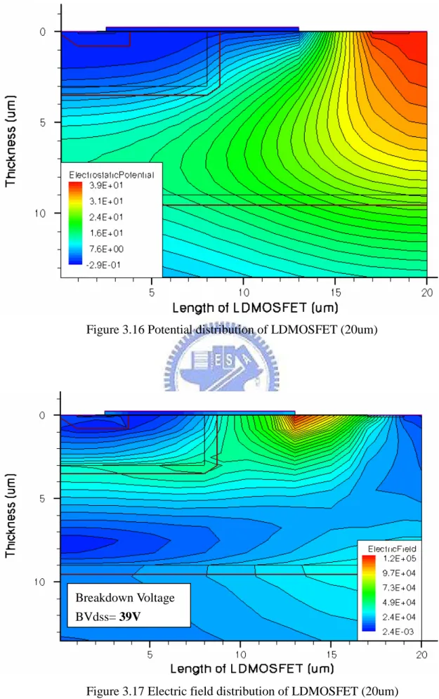
Peak electric field of gate edge is form, and observe equipotential line of gate edge which is crowded as shown in Figure 3.16 [10]. When power device is off-state, the drain to gate have potential (Vdg). To estimate electric field (E) of gate edge (see Figure 3.17): ˆ dg V E a L = − r ( 3.1 )
Where L is distant of gate to drain, which is proportional to length of drift region. When length of drift region is too short, to cause electric field of gate and drain that is too large. Avalanche breakdown is easy to take place in under gate edge, this is because RESURF LDMOSFET can’t design short drift region.
The optimal case is obtained when the depletion region extends equally in the N-drift and P substrate regions. If the lateral distance is sufficient, breakdown occurs vertically in the semiconductor bulk under the N+ region. As shown in Figure 3.5 the electric field distribution of the optimized lateral diode, where the peak electric field can be seen under three position (source, gate, and drain edge). As shown in Figure 3.4 is not RESURF of LDMOSFET, and cause breakdown voltage become smaller.
Figure 3.16 Potential distribution of LDMOSFET (20um)
Figure 3.17 Electric field distribution of LDMOSFET (20um) Breakdown Voltage
3.3 Advantage of Trench LDMOSFET
The main structure in this thesis, drift region of conventional LDMOSFET add oxide trench, is called Trench LDMOSFET as shown Figure 3.18. We choose silicon dioxide to do material of trench, which is high critical electric field (107V/cm), and it is 33.3 times electric field of silicon. Therefore, it bears higher electric field of gate edge. Silicon dioxide and silicon match pretty well and process easily.
Figure 3.18 Structure of Trench LDMOSFET
In order to verify oxide trench to avoid breakdown of gate edge, and observe off state in Trench LDMOSFET which is 159V electric field of breakdown voltage. Trench LDMOSFET has a part of surface that is filled with silicon dioxide. Figure 3.19 is electric field of Trench LDMOSFET, and shows to keep away from gate edge, electric field is becoming smaller. Interface of silicon and silicon dioxide have great energy gap. When Trench LDMOSFET is on state, electron can not punch through silicon dioxide,
P
+N
+N
+Poly-silicon
Oxide
P-base
N-Drift Region
(epi layer)
P-substrate
Source
Drain
Gate
P
+N
+N
+Poly-silicon
Oxide
P-base
N-Drift Region
(epi layer)
P-substrate
Source
Drain
Gate
and electron that need detour silicon dioxide of trench move to drain. Design of oxide-trench etch part of drift region, and cause cross-section area of electron current which is getting smaller. Oxide trench cause resistance of drift region that is becoming larger. If drift region increases concentration, drain reduces the peak value of electric field (see Figure 3.20). The result of simulation prove this conjecture.
Figure 3.19 Electric field of Trench LDMOSFET Breakdown Voltage
BVdss= 209V
Ron,sp= 47.6mΩ-cm2
Epi concentration ( 6E14 cm-3 )
Figure 3.20 Electric field of Trench LDMOSFET
3.4 Design of Trench LDMOSFET
For power device, a good device owns characteristic of large breakdown voltage and small on-resistance, and at the same time a size of cell pitch designs emphasis on the whole efficiency, in other words, the power device is smaller, it will save us a lot of cost. A structure parameter of device is quite a few, it is very difficult to use Full factorial analysis. In order to understand change of physical property, and decide to adopt one factor at a time. Finally, we change parameter to observe relationship between Trench LDMOSFET and LDMOSFET.
Breakdown Voltage BVdss= 159V
Ron,sp=11.3mΩ-cm2
Epi concentration ( 3E15 cm-3 )
Trench LDMOSFET improves avalanche breakdown of LDMOSFET in gate edge. Therefore, designing trench to increase breakdown voltage and reduce on-resistance effect.
3.4.1 Parameter definition
Designing power device has two parameter of electric property that is important, and defines breakdown voltage and on-resistance.
3.4.1.1 Breakdown voltage
In general, device operation is off state (Vg=0V), and increases drain voltage by degrees. When drain current is getting to 1x10⁻⁶ A, this device stands for breakdown state. We use simulation soft of device electric property (ISE TCAD_Dessis) [11,12,13] which is two-dimension simulation program, width of device is defined 1um, the result of drain current (Id) is unit width of drain current (Id/1um). Because width of normal power device is about 10mm, we increase drain voltage make unit width of drain current (over1x10-10A/um) which enter breakdown state. At this time, drain voltage is also breakdown voltage. Breakdown voltage of device (as shown Figure 3.21) is 159V.
Figure 3.21 Breakdown voltage of Trench LDMOSFET
3.4.1.2 On-resistance
The on-resistance [14] of a Power MOSFET is a very important parameter because it determines how much current the device can carry for low to medium frequency applications. After being turned on, the on-state is defined simply as its on-state voltage divided by on-state current. When conducting current as a switch, the power dissipation in the power MOSFET during current conduction is given by:
2
D D D D on
P =I V =I R ( 3.2 )
159V
Expressed in terms of the chip area (A): 2 2 , , D D on D on sp on sp on P J AR J R A R AR = = = ( 3.3 )
Where (PD/A) is the power dissipation per unit area; JD is the on-state current density; and Ron,sp is the specific on-resistance, defined as the on-resistance per unit area. These expressions are based upon the assumption that the power MOSFET is operated in its linear region at a relatively small drain bias during current conduction. The region of operation in Figure 3.22 have been labeled linear and saturated. To understand the difference, recall that the actual current path in a MOSFET is horizontal through the channel created under the gate oxide and then vertical through the drain. In the linear region of operation, the voltage across the MOSFET channel is not sufficient for the carriers to reach their maximum current density. The static on-resistance (Ron), defined simply as VDS/IDS, is a constant. To adopt VGS=5V and VDS=1V, and get drain current to calculate on-resistance. Thus specific on-resistance (Ron,sp) is 11.3mΩ-cm2.
Figure 3.22 Output Characteristics of Trench LDMOSFET
VGS=5V
VDS=1V
3.4.2 Fabrication of Trench LDMOSFET
Oxide trench can improve characteristic of LDMOSFET, and change structure of LOCOS (LOcal Oxidation Of Silicon) gain better efficiency. The process flow of Trench LDMOSFET is as shown in Table3.1 [15].
Table 3.1 Process procedure of Trench LDMOSFET
Process
procedure
Process Description
Mask
No.
Schematic
Diagram
1 Lightly doped P-type substrate wafer<100> Figure 3.23 2 Growth of a heavily doped N-type epitaxiallayer
Figure 3.24
3 P-base creation with boron implantation and diffusion
1 Figure 3.25
4 Reactive ion etching(RIE) is performed to form trenches
5 Trench is filled with silicon dioxide 6 To polish surface by CMP
2 Figure 3.26
7 Depositing silicon dioxide(350Å) Figure 3.27
8 Depositing Poly-silicon layer(2000Å) to form gate patterning
3 Figure 3.28
9 Arsenic implantation is carried out to form S/D region
4 Figure 3.29
10 BF2 implantation is performed to create P-base
contact
5 Figure 3.30
11 Depositing silicon dioxide
12 Contact window is opened for source/gate/drain
Figure 3.31
13 Aluminum is sputtered 14 Metal patterning
6
Figure 3.23 Process Flow Chart
Figure 3.24 Process Flow Chart
Figure 3.25 Process Flow Chart PSubstrate
1. <100> P type wafer
PSubstrate N-Drift Region
2. To Grow N type epi layer
3. Mask 1
-boron implantation and diffusion to form P-base PSubstrate
N-Drift Region Boron
Figure 3.26 Process Flow Chart
Figure 3.27 Process Flow Chart
Figure 3.28 Process Flow Chart PSubstrate
N-Drift Region
P-Base 4. Mask 2
-To etch trench To fill oxide in trench Using CMP to polish surface 5. To deposite oxide in surface PSubstrate N-Drift Region P-Base Photo-resistance (PR) Silicon dioxide Silicon dioxide Silicon dioxide PSubstrate N-Drift Region
P-Base 6. To deposite polysilicon
in surface Mask 3 -Gate patterning Photo-resistance (PR) Silicon dioxide Polysilicon Silicon dioxide
`
Figure 3.29 Process Flow Chart
Figure 3.30 Process Flow Chart
7. Mask 4 -Arsenic implantation to form Source/Drain Photo-resistance (PR) Silicon dioxide Polysilicon Silicon dioxide PSubstrate N-Drift Region P-Base Arsenic Arsenic 8. Mask 5 -BF2 implantation to form base contact
Photo-resistance (PR) Silicon dioxide Polysilicon Source N+ / Drain N+ BF2 PSubstrate N-Drift Region P-Base Silicon dioxide
Figure 3.31 Process Flow Chart
Figure 3.32 Process Flow Chart
9. To deposite oxide Mask 6 -Contact etching Photo-resistance (PR) Polysilicon Source N+ / Drain N+ Silicon dioxide Silicon dioxide PSubstrate N-Drift Region P-Base PSubstrate N-Drift Region
P-Base 10. To deposite metal (Al)
Reuse Mask 6 -Metal patterning Photo-resistance (PR) Polysilicon Source N+ / Drain N+ Silicon dioxide Silicon dioxide Metal (Al)
3.4.3 Trench design
For LDMOSFET, breakdown voltage is positive relation with the drift region, and gains high breakdown voltage to make the longer drift region, which reduces cell pitch. This is disadvantage of LDMOSFET, which can’t save cost and reduce device area. Trench LDMOSFET [16,17,18,19] can reduce electric field of gate edge as shown in Figure 3.19, and can decrease length of the drift region. According to equation 3.1, electric field of gate edge is positive proportional to length of the drift region. When length of the drift region decreases, it causes electric field to become large as shown in Figure 3.17. Therefore, better trench design reduces electric field of gate edge.
3.4.3.1 Depth of Oxide Trench
In order to understand effect of oxide trench on Trench LDMOSFET, we adopt to analyze parameter of LDMOSFET, concentration of the drift region is 7E14cm-3, depth of the drift region is 10um, concentration of P-base is 1E15 cm-3, and depth of P-base is 5um. To use these conditions to change depth of oxide trench, and observe breakdown state. According to Figure 3.33 and Figure 3.34, depth of oxide trench is getting deep, breakdown voltage is also becoming large. In other words, oxide trench increases depth, the drift region is getting thin, electron pass through cross sectional area, which is becoming small, resistance of the drift region becomes large, and on-resistance is getting large.
Figure 3.33 Breakdown voltage of Trench depth
Figure 3.34 On-resistance of Trench depth
0 20 40 60 80 100 120 0 1 2 3 4 5 6 7 8 9 10
Trench depth (um)
O
n
-r
es
is
ta
n
ce
(
m
Ω
-c
m
2)
Trench width= 8um Trench width= 10um Trench width= 12um Trench width= 14um 0 50 100 150 200 250 300 350 0 1 2 3 4 5 6 7 8 9 10
Trench depth (um)
B
re
ak
d
o
w
n
v
o
lt
ag
e
(V
)
Trench width= 8um Trench width= 10um Trench width= 12um Trench width= 14um
3.4.3.2 Position of Oxide Trench
The above-mentioned result point to breakdown voltage and on-resistance are controlled by depth of Trench LDMOSFET. After oxide trench analyzes depth, to discuss position of oxide trench, and understand breakdown voltage and on-resistance.
We use parameter of trench depth, and set trench depth (T) is equal to 5um as shown in Figure 3.35, trench width is 10um (L1+L2), to change L1 length (gate edge to left size of oxide trench), which is 0.5um, 1um, 1.5um, 2um, 2.5um, and 3um. L2 (gate edge to right size of oxide trench) length is changed by L1, the result is in Figure 3.36 and Figure 3.37. When L1 is getting large, breakdown voltage change just a little, on-resistance change just a little like breakdown voltage.
Figure 3.35 Structure parameter of Trench LDMOSFET
P
+N
+N
+Poly -silicon
Oxide
P-base
N-Drift Region
(epi layer)
P-substrate
Source
Drain
Gate
P
+N
+N
+Poly -silicon
Oxide
P-base
N-Drift Region
(epi layer)
P-substrate
Source
Drain
Gate
L1
L2
T
P
+N
+N
+Poly -silicon
Oxide
P-base
N-Drift Region
(epi layer)
P-substrate
Source
Drain
Gate
P
+N
+N
+Poly -silicon
Oxide
P-base
N-Drift Region
(epi layer)
P-substrate
Source
Drain
Gate
L1
L2
T
Lgate
Figure 3.36 Breakdown voltage of L1 length
Figure 3.37 On-resistance of L1 length
94 106 107 107 108 108 92 94 96 98 100 102 104 106 108 110 0 0.5 1 1.5 2 2.5 3 3.5
Length of L1 (um)
B
re
ak
d
o
w
n
v
o
lt
ag
e
(V
)
Trench depth= 5um
36.6 36.1 36 36 35.9 35.6 35.4 35.6 35.8 36 36.2 36.4 36.6 36.8 0 0.5 1 1.5 2 2.5 3 3.5
Length of L1 (um)
O
n
-r
es
is
ta
n
ce
(
m
Ω
-c
m
3.4.3.3 Length of Polysilicon Gate
According to simulation result of trench parameter, we adjust L1 (1um), trench width (L1+L2=10um), and trench depth (5um) to change length of polysilicon gate (Lgate), and observe breakdown voltage and on-resistance as shown in Figure 3.38 and Figure 3.39. When length of polysilicon gate is getting longer, this device increases breakdown voltage and reduces on-resistance. Because polysilicon gate edge is far away from the source, potential is on Silicon and Silicon dioxide, the drain (N+) and electric field of N drift region is too small to take place breakdown, and get higher breakdown voltage. The positive bias of polysilicon gate attracts electron to form channel of lower resistance on surface, while length of polysilicon gate is getting longer, this channel is also becoming long, and causes on-resistance to decrease.
Figure 3.38 Breakdown voltage of Polysilicon Gate length
Figure 3.39 On-resistance of Polysilicon Gate length
106 132 161 78 78 134 60 80 100 120 140 160 180 10 11 12 13 14 15 16 17 Length of Polysilicn Gate (um)
B re ak d o w n v o lt ag e (V ) 53.2 41.6 35.9 34 32.4 32.3 0 10 20 30 40 50 60 10 11 12 13 14 15 16 17
Length of Polysilicon Gate (um)
O n -r es is ta n ce ( m Ω -c m 2)
3.5 Efficiency Analysis
For application of LCD display, To design a power MOSFET, reverse voltage is 150V and lower on-resistance, to use LDMOSFET and Trench LDMOSFET technology. According to the above-mentioned discussion, we choose to use Trench LDMOSFET to conform to characteristic of power device, and find a parameter set of Trench LDMOSFET, which compares efficiency with LDMOSFET. Efficiency equation of power MOSFET is composed of breakdown voltage and on-resistance. This equation is as follows. 2 _ ( ) _ Re tan Breakdown Voltage V Efficiency On sis ce m cm = Ω − ( 3.4 )
By equation 3.4 [20], efficiency of power MOSFET determines breakdown voltage and on-resistance whether better or worse device. If efficiency is getting large, it shows better power MOSFET, on the other hand, efficiency is getting small, it shows worse power MOSFET.
Trench LDMOSFET compares data of efficiency with LDMOSFET. It is shown in Table 3.2. Parameter of Trench LDMOSFET is 5 times efficiency of LDMOSFET, breakdown voltage is 159V, specific on-resistance is 11.3 mΩ-cm2, this is a better
Table 3.2 Parameter comparison of Power MOSFET
Power MOSFET
Parameter Condition Breakdown Voltage ( V )
On-resistance ( mΩ-cm2 )
Efficiency
LDMOSFET
Cell pitch ( 50um )
Concentration of P-Substrate ( 1E14cm-3 )
Concentration of Drift region ( 4E14cm-3 )
Depth of Drift region ( 9um ) Concentration of P-Base ( 1E15cm-3 )
Depth of P-Base ( 3um ) Source(N+), Drain(N+) ( 1E17cm-3 )
Length of Polysilicon Gate ( 13um )
153
56.3
2.7
Trench LDMOSFET
Cell pitch ( 30um ) P-Substrate ( 1E14cm-3) Concentration of Drift region ( 3E15cm-3 )
Depth of Drift region ( 5um ) Concentration of P-Base ( 6E15cm-3 )
Depth of P-Base ( 2um ) Source(N+), Drain(N+) ( 1E17cm-3 )
Length of Polysilicon Gate ( 13um )
Depth of Trench ( 2.5um ) Width of Trench ( 10um )
CHAPTER 4
Optimal design of Trench LDMOSFET
4.1 Introduction to experiment methods
In order to gain optimal design, we can choose 3 kinds of experiment methods commonly. Experiment methods include trial-and-error, one factor at a time, and Taguchi Methods. A well planned set of experiments, in which all parameters of interest are varied over a specified range, is a much better approach to obtain systematic data. Mathematically speaking, such a complete set of experiments ought to give desired results. Usually the number of experiments and resources (materials and time) required are prohibitively large. Often the experimenter decides to perform a subset of the complete set of experiments to save on time and money. However, it does not easily lend itself to understanding of science behind the phenomenon. The analysis is not very easy (though it may be easy for the mathematician/statistician) and thus effects of various parameters on the observed data are not readily apparent. In many cases, particularly those in which some optimization is required, the method does not point to the best settings of parameters. A classic example illustrating the drawback of design of experiments is found in the planning of a world cup event, say football. While all matches are well arranged with respect to the different teams and different venues on different dates and yet the planning does not care about the result of any match (win or lose). Obviously, such a strategy is not desirable for conducting scientific experiments.