國
立 交 通 大 學
材料科學與工程學系
博士論文
無電鍍沉積薄膜應用於銲錫擴散阻障層之研究
Investigation of Electroless Deposited Films as the Diffusion
Barrier of Pb-Sn Solder
學生姓名:梁沐旺(Muh-Wang Liang)
指導教授:謝宗雍 博士(Dr. Tsung-Eong Hsieh)
無電鍍沉積薄膜應用於銲錫擴散阻障層之研究
學生:梁沐旺 指導教授:謝宗雍 博士 國立交通大學 材料科學與工程學系摘
要
本研究以無電鍍與焊錫擴散鍵結等兩種製程,取代深次微米半導體金屬墊層 (UBM)元件物理氣相沉積製程(PVD)階梯覆蓋性不佳的現象,使金屬墊層(UBM)仍具 良好的元件鍵結附著力,並兼具擴散阻障、潤濕及保護作用,可達覆晶構裝低成本、 高密度與優良電性的需求。 本研究進行無電鍍製程沉積實驗,其等向沉積成長元件之金屬墊層,可解決元件 鍍膜階梯覆蓋性不佳的問題。首先在氮化鋁基板上製作無電鍍鎳/銅雙層線路及凸 塊,由元素線掃描結果顯示,錫無法突破鎳層之阻絕,證實鎳層是一良好的擴散阻絕 層;其次,本實驗以無電電鍍沉積技術(Electroless Plating)在矽晶基板上製作無電 電鍍鈷磷(Co-P)合金薄膜,再以電鍍方式沉積錫鉛(Pb-Sn)銲料於其上,用以探 討無電鍍鈷磷薄膜做為銅製程覆晶接合(Flip-chip Bonding,FC)凸塊底部金屬化 (Under Bump Metallurgy,UBM)之應用可行性。X 光繞射(X-ray Diffraction,XRD) 顯示無電鍍鈷膜主要應由非結晶與微晶(microcrystalline)混合組成。元素線掃描分 析結果顯示,在錫、銅及鈷之相互擴散反應過程中,當做為潤濕層的銅被完全消耗掉之後,錫仍只在鈷磷鍍層與銲錫的界面處;經250°C、24 小時之熱處理後,錫無法穿 透鈷磷層的阻擋,而底層的銅亦無法擴散至銲錫層中,證實無電鍍鈷磷層可同時做為 銅導線與銲錫凸塊之擴散阻障層(Diffusion Barrier),而其阻擋能力主要由高磷含量 之初鍍鈷層形成之非晶質結構所提供。進行無電鍍鎳、銅與氮化鋁基板之拉桿黏著強 度試驗,顯示鎳和銅之間黏著力亦大於761 kg/cm2,皆符合電路元件之黏著強度之要 求。以無電電鍍搭配微影成像及蝕刻技術,在基板上製作無電鍍鎳或鈷/銅雙層線路 及凸塊;另藉由電鍍方法沉積錫鉛於無電鍍鎳/銅上,用以模擬鎳銅凸塊與銲錫球產 生之界面反應,無電鍍法所沉積的鎳磷(Ni(P))與鈷磷(Co(P))薄膜具有良好階梯覆 蓋性,可同時做為銅製程之銅導線與銲錫凸塊之擴散阻障層,此Ni 或 Co 層阻擋能力 主要由高磷含量之鈷層形成之非晶質結構所提供。 本研究另提出擴散接合的製程,乃一種低溫金屬銲錫擴散鍵結的構裝接合技術, 這篇論文便研此新穎的構裝接合技術。將多層薄膜Cu/Ti/Si 與 Au/Cu/Al2O3在攝氏250 度至400 度間以焊錫鍵結,實驗研究結果顯示在結合界面將產生金屬界面化合物 η-(Cu0.99Au0.01)6Sn5與δ-(Au0.87Cu0.13)Sn,此金屬界面化合物的成長受限於擴散控制, 可減少焊接的缺陷產生(如凝結裂縫或氣孔等),而且期抗拉強度可達 132 kg/cm2 ,達 無鉛構裝產業應用價值。 依據這些實驗結果顯示無電鍍與焊錫擴散接合法確實是光電半導體覆晶金屬墊 層可應用的優良技術。
Investigation of Electroless Deposited Films as the Diffusion
Barrier of Pb-Sn Solder
Student: Muh-Wang Liang Advisor: Prof. Tsung-Eong Hsieh
Department of Materials Science and Engineering National Chiao-Tung University
Abstract
Under bump metallization (UBM) provides good adhesion between the bonding pads and the bumps, and serves as a diffusion barrier, wetting, and protective layer for flip-chip bonding. Both Au and Cu are so-called fast diffusers in Sn, and can diffuse very long distances in Sn in a relatively short time.. All of UBM metals are in general deposited by physical vapor deposition (PVD). However, as being used in the recent deep
sub-micron Cu-IC process, the PVD suffers from poor step coverage. Numerous efforts have been made to solve this difficulty.
To solve the step coverage problems, a new idea was provided that the diffusion barrier layer in the Cu-IC process can be formed by using an electroless plating method. At first, the application of electroless copper/nickel (Cu/Ni) films on aluminum nitride (AlN) substrates was explored. The Ni film remained a mixture of amorphous and
microcrystalline structures, and the Cu film was polycrystalline. Subsequent Pb-Sn solder bumping experiments indicated the amorphous Ni(P) film was a good diffusion barrier layer since Sn could not diffuse through it. The electroless Ni(P) layer has a step coverage and simultaneously serve as a diffusion barrier of Cu interconnects and UBM structure of
flip-chip Cu-ICs. Pull-off tests revealed that the Cu/Ni films strongly adhered on both types of AlN substrates and that the adhesion strength exceeded 761 kg/cm2. Next, electroless plating technique was utilized to prepare the cobalt-phosphorous Co(P) thin film to serve as the diffusion barrier layer of lead-tin solder. The x-ray diffraction (XRD) in conjunction with composition analyses revealed that the electroless Co(P) layer was a mixture of amorphous and nanocrystalline structures. The fact that Sn and Cu underlayer could not penetrate Co layer after such a liquid-state annealing evidenced that the Co(P) layer may simultaneously serve as a diffusion barrier interlayer dielectrics and UBM for flip chip copper (Cu) ICs.
The multi-layer thin-film systems of Cu/Ti/Si and Au/Cu/Al2O3 were
diffusion-soldered at temperatures between 250°C and 400°C by inserting an Sn thin-film interlayer. Experimental results showed that a double layer of intermetallic compounds η-(Cu0.99Au0.01)6Sn5/δ-(Au0.87Cu0.13)Sn were formed at the interface. Kinetics analyses
reveal that the growth of intermetallics was diffusion-controlled. The activation energies as calculated from Arrhenius plots of the growth rate constants for (Cu0.99Au0.01)6Sn5 and
(Au0.87Cu0.13)Sn are 16.9 kJ/mol and 53.7 kJ/mol, respectively. The satisfactory tensile
strength of 132 kg/cm2 could be attained under the diffusion bonding condition of 300°C for 20 min for Cu/Ti/Si and Au/Cu/Al2O3.
Results in these experiments demonstrate that electroless plating and diffusion soldering are indeed excellent technology for UBM structure of flip-chip ICs.
Acknowledgements
This work was supported by: (i) the Department of Industrial Technology, Ministry of Economics Affairs of the ROC under TDPA (Technology Development Program for Academic) contract No. 92-EC-17-A-05-S1-020, 95-EC-17-A-05-S1-020, (ii) the National Science Council of the ROC under contract No. NSC91-2216-E-009-031, NSC93-2216-E-009-008, NSC94-2216-E-009-026, and (iii) Mechanical and Systems Research Laboratories / Industrial Technology Research Institute.
Contents
Abstract (in Chinese)……….………..I
Abstract (in English)……….……….III
Acknowledgements……….V
Contents……….VI
Table lists………..VIII
Figure Captions...IX
Chapter 1 Introduction
1-1 Motivation...1 1-2 Thesis Outline...4Chapter 2 Literature Review
2-1 Diffusion soldering…...8 2-2 Electroless Ni plating...8 2-3 Electroless cobalt plating ………10
Chapter 3 Experimental
3-1 Experimental Method for Thin-Film Reactions during Diffusion
Soldering of Cu/Ti/Si and Au/Cu/Al2O3 with Sn Interlayers……….15
3-2 Experimental Method for Electroless Copper/Nickel Films Deposited on AlN Substrates………16 3-3 Experimental Method for Electroless Cobalt-Phosphorous Layer and
Its Diffusion Barrier Properties of Pb-Sn Solder………20
Chapter4 Results and Discussion
4-1Thin-Film Reactions during Diffusion Soldering of Cu/Ti/Si and Au/Cu/Al2O3 with Sn Interlayers ………..244-2 Electroless Copper/Nickel Films Deposited on AlN Substrates ……33
4-3 Electroless Cobalt Layer and Its Diffusion Barrier Properties of Pb-Sn Solder ……….51
Chapter 5 Conclusions ……….
62Prospective research ………..……….
.64References ………
66Vita (in Chinese)...
71Table Lists
Table 3.1. Compositions of sensitization and activation solution………...18 Table 3.2. Solution for roughening, sensitization, activation and the immerse time……..21 Table 3.3. Compositions of electroless plating bath………22 Table 4.1. Thicknesses of intermetallic compounds formed during diffusion soldering
between Cu/Ti/Si and Au/Cu/Al2O3 with Sn interlayers………28
Table 4.2. Growth rate constants of intermetallic compounds formed during diffusion soldering between Cu/Ti/Si and Au/Cu/Al2O3 with Sn interlayers……….29
Table 4.3. Compositions of electroless Ni on polished AlN surface. (unit : wt%)………..45 Table 4.4. Compositions of electroless Ni on unpolished AlN surface. (unit : wt%)……..46 Table 4.5. Pull-off test results of electroless Ni on polished AlN substrate………47. Table 4.6 Pull-off test results of electroless Ni/Cu on polished AlN substrate………48 Table 4.7. Average thickness of plated Co(P) layer……….52 Table 4.8. EDX phosphorous contents with respect to different deposition times………..55 Table 4.9.EDX analysis of IMCs produced under different duration of thermal treatment.60
Figure Captions
Fig. 3.1:The scheme of diffusion soldering for Cu/Ti/Si and Au/Cu/Al2O3 with Sn
interlayers………16
Fig. 3.2 Process flow of AlN substrate metallization [39-41]………..17
Fig. 3.3 Flow chart of Co(P) specimen preparation………..22 Fig. 4.1:The morphology of intermetallic compounds formed after diffusion soldering
between Cu/Ti/Si and Au/Cu/Al2O3 at 300°C for 20 min with Sn interlayers….25
Fig. 4.2:The Au, Sn and Cu concentrations across the multi-layers of the diffusion soldered specimen (from Fig. 4.1)………..25 Fig. 4.3:The average thickness (∆x) of (Cu0.99Au0.01)6Sn5 intermetallic compounds formed
during diffusion soldering between Cu/Ti/Si and Au/Cu/Al2O3 with Sn
interlayers……….27 Fig. 4.4:The average thickness (∆x) of (Au0.87Cu0.13)Sn intermetallic compounds formed
during diffusion soldering between Cu/Ti/Si and Au/Cu/Al2O3 with Sn
interlayers……….27 Fig. 4.5:The Arrhenius plots of growth rate constants (k) for (Cu0.99Au0.01)6Sn5 and
(Au0.87Cu0.13)Sn intermetallic compounds formed during diffusion soldering
between Cu/Ti/Si and Au/Cu/Al2O3 with Sn interlayers………..28
350°C. Sn(l)/Au(s) reacts much more quickly than Sn(l)/Cu(s)………32
Fig. 4.7:The tensile strengths (σ) of Cu/Ti/Si wafer diffusion-soldered with Au/Cu/Al2O3
substrates at various temperatures for 20 min using an Sn thin-film interlayer..33 Fig. 4.8: Surface morphology of polished AlN surface after etching for (a) 0 min, (b) 30
min, (c) 60 min, and (d) 120 min……….34 Fig. 4.9: Surface morphology of unpolished AlN surface after etching for (a) 0 min, (b) 30
min, (c) 60 min, and (d) 120 min………35 Fig.4.10: Variation in AlN surface roughness with etching time………..35 Fig.4.11: Surface morphologies of electroless Ni plated on polished AlN substrates for (a)
0.5 min, (b) 1 min, (c) 4.5 min, and (d) 26.5 min……….36 Fig.4.12: Surface morphologies of electroless Ni plated on unpolished AlN substrates for
(a) 0.5 min, (b) 1 min, (c) 4 min, and (d) 30 min……….38 Fig. 4.13:Illustration of grain growth on (a) polished and (b)unpolished AlN substrates.38 Fig. 4.14: Cross-sectional view of EN layer plated for 3 min on (a) polished and (b)
unpolished AlN substrates………39 Fig. 4.15: Surface morphologies of electroless Cu plated on (a) polished and (b)
unpolished AlN substrates plating for 90 min………..39 Fig. 4.16: Resistivities of electroless (a) Ni and (b) Cu deposited on polished and
unpolished AlN substrates………41 Fig. 4.17 XRD pattern of Ni/AlN (a) before and (b) after 250°C 1 h annealing ( :
AlN; :Ni)………..43 Fig. 4.18: XRD pattern of Cu /Ni /AlN (a) before and (b) after 250°C 1 h annealing. ( :
AlN; :Cu)………44 Fig. 4.19: SIMS depth profile of EN layer plated on polished AlN substrate for 2 min.46 Fig. 4.20: Flip chip bonding of GaAs PHEMT IC on AlN substrate...50 Fig. 4.21: SEM cross-sectional view of EN/AlN interfaces and corresponding line
scanning EDS analysis (a) before 250°C annealing and (b) after 250°C 2 h annealing………50 Fig. 4.22: Thickness of electroless plating Co(P) layer vs. deposition time……….52 Fig. 4.23: Surface morphologies of Co layers deposited at different pH values: (a) pH =
7.5; (b) pH = 8.0; (c) pH = 8.5; (d) pH = 9.0………..54 Fig. 4.24:Average phosphorous content of electroless Co(P) analyzed by AES…………56 Fig. 4.25:XRD analysis performed on Co(P) films of different deposition times……….57 Fig. 4.26:XRD analysis performed on Co(P) films of 30 min deposition time………….58 Fig.4.27:Cross-sectional SEM view of specimen interfaces and corresponding line
scanning EDX analyses after 250°C (a) 6-hr and (b) 24-hr annealing………..61 .
Chapter 1 Introduction
1.1 Motivation
In recent years, the state-of-the-art semiconductor related techniques have developed rapidly and competitively. All the leading manufacturers have made efforts in developing IC components with lower costs, smaller sizes, and higher performances. In addition to the leading technologies for 12-inch silicon wafer and deep sub-micron fabrication, the package technology has become a more important issue as well. Conventional package techniques such as lead frame package (LFP), ball grid array (BGA) package, and tape automatic bonding (TAB) package have been improved to allow IC components to have smaller sizes, higher throughput and better performances. Today, there are at least three popular chip-level connections, namely, face-up wire bonding, face-up tape-automated bonding, and flip chip. Among these three technologies, flip chip provides the highest packaging density and electronic performance and the lowest packaging profile which will meet the demand for packaging at ever higher frequencies. Therefore, more and more companies and universities have devoted themselves to the development of flip chip packaging for semiconductor. The flip chip interconnect is based on three fundamental building blocks, the bumps on the chip, the substrate and the method to attach the chip to the substrate. Among the various types of bumps, the solder bump is by far the most common and reliable for Flip Chip bonding, especially the eutectic lead/tin solder.
Ceramic material has excellent characters of heat conduction and electric
insulation, and the characters can be adjusted by modulating its chemical compositions, so the application of ceramic material is very extensive in electric package; it not only is the common material of interposer and seal cap, but also can be used to fabricate Multilayer Interconnection Substrate for high density package when cooperating with thick film metallization process. Aluminum oxide (Al2O3) and aluminum nitride (AlN) are common material of ceramic package substrate; wherein AlN has Wurtzite structure, so AlN
substrate has better heat conductivity (AlN: 230 W/m°K, Al
2O3: 20 W/m
°K, Si: 150
W/m°K, GaAs: 50 W/m°K), lower dielectric constant (in 1MHz, AlN: 8.8, Al
2O3: 8.5),
approximate thermal expansion coefficient with GaAs (AlN: 4.5 ppm/°K, Al
2O3: 7.3
ppm/°K, Si: 2.6 ppm/°K, GaAs: 5.73 ppm/°K), and better electrical and mechanical properties; moreover, it is compatible with all thin/thick film metallization process. Aluminum nitride is an important substrate material for electronic packaging due to its good electrical, mechanical and heat conduction properties. It not only serves as a good heat sink for GaAs MHEMTs, but also hosts all the passive circuit components such as transmission lines, resistors, capacitors.
Under bump metallization (UBM) provides good adhesion between the bonding pads and the bumps, and serves as a diffusion barrier, wetting, and protective layer for flip-chip bonding. There are mainly four types of diffusion barrier layer: sacrificial barriers,
stuffed barriers, passive compound barriers and amorphous barriers. [1] The most common materials used in UBM as diffusion barrier layer are refractory metals, such as titanium (Ti), tungsten (W), and molybdenum (Mo), and the alloy thereof. All of these metals have superior diffusion barrier capability at high temperatures and are in general deposited by physical vapor deposition (PVD). However, as being used in the recent deep sub-micron Cu-IC process, the PVD suffers from poor step coverage. Numerous efforts have been made to solve with this difficulty, which comes up with the idea that the diffusion barrier layer in the Cu-IC process can be formed by using an electroless plating method[2,3] and presently the electroless plated nickel (Ni) is most commonly adopted for UBM [4-7].
Because the PVD suffers from poor step coverage, numerous efforts have been made to solve this difficulty. Electroless plating is based on the theorem of
oxidation-reduction, making metal proceed selective deposition on the wanted plating surface. The Electroless plating technology on the surface coverage of tradition metal device has been applied for a long time, and is tried to apply on the semiconductor wafer fabrication to reduce fabrication cost and improve the competitiveness; the main character of electroles plating is that it can process a great deal of wafers, such as 25pcs or 50pcs in the same time by using cassette, to relatively reduce the whole process time. So far electroless plating technology has been widely applied to electronic industry due to it simple process and low cost features. Nickel (Ni) and cobalt (Co) are the most common metals that could be deposited using electroless plating process. The electroless metal has
been utulized as a diffusion barrier for multilayer microelectronic structure, it is also a good barrier metal to inhibit the interdiffusion between the solder bump and metallization of integrated circuits (ICs). This technique easily allows the parallel processing of multiple wafers so that it can lead to a high throughput. Therefore the electroless process is a promising technology for flip chip packaging applications because a low cost is always a key issue in production. To solve the step coverage problems, the electroless plating method was provided.
Diffusion soldering (also known as solid-liquid interdiffusion bonding) is a novel joining technique based on the principle of isothermal solidification. A low melting, metallic thin-film interlayer is employed in the process, which melts at low temperatures and reacts rapidly with both high-melting (HT1 and HT2) layers or substrates
to form intermetallic compounds (IMs). Since the intermetallic compounds formed at the interfaces possess much higher melting points than the original low-melting interlayer, a special feature of bonding at lower temperatures and usage at higher temperatures can be achieved [8]. Such a superior characteristic enables diffusion soldering to broaden its application potentials in the electronics industry [9-11].
1.2 Thesis Outline
According to the underlying principle of the diffusion soldering process, it is obvious that interfacial reactions play a key role in the joining efficiency of this technique. The
effort of this study is thus concerned with the intermetallic compounds formed at the interfaces and their growth kinetics during the diffusion soldering of the multi-layer thin-film systems bonded onto Si wafers and Al2O3 substrates. In addition, the tensile
strengths of the diffusion-soldered specimens are evaluated. In the chapter 4-1, I studied thin-film reactions during diffusion soldering of Cu/Ti/Si and Au/Cu/Al2O3 with Sn
interlayers. The multi-layer thin-film systems of Cu/Ti/Si and Au/Cu/Al2O3 were
diffusion-soldered at temperatures between 250°C and 400°C by inserting an Sn thin-film interlayer. Experimental results showed that a double layer of intermetallic compounds η-(Cu0.99Au0.01)6Sn5/δ-(Au0.87Cu0.13)Sn was formed at the interface. Kinetics analyses
revealed that the growth of intermetallics were diffusion-controlled.
In recent years, the fabrication techniques for both ultra large scale integrated circuits (ULSI) and liquid crystal displays (LCDs) tend towards lower temperatures in order to avoid degradation of the device characteristics due to the thermal stress on the thin films. Owing to novel low-temperature related techniques, various low melting-point substrates such as glass substrates and plastic substrates are suitable for use in growth of high-quality thin films with low thermal stress at low temperatures. In the chapter 4-2, we studied the electroless copper/nickel (Cu/Ni) films deposited on aluminum nitride (AlN) substrates applied to high-frequency power GaAs device packaging. Experimental results showed metal films deposited on polished AlN surfaces possess flatter surface, finer grain structure, and lower resistivity than those on unpolished surfaces. The Ni film remained a
mixture of amorphous and microcrystalline structure, and the Cu film was polycrystalline. Subsequent Pb-Sn solder bumping experiments indicated the amorphous Ni(P) film was a good diffusion barrier layer since Sn can not diffuse through it.
Since the capability of electroless Co(P) as a barrier layer in UBM structure is yet to explore, we hence carried out this study in order to investigate its feasibility to serve both as the barrier layer of interlayer dielectrics and UBM for flip-chip Cu-ICs. The chapter4-3 tried to explain the investigation of electroless cobalt-phosphorous layer and its diffusion barrier properties of Pb-Sn solder. The capability of cobalt-phosphorous (Co(P)) layer, which was grown via electroless plating process, to serve as the diffusion barrier of lead-tin (PbSn) solder was investigated. The x-ray diffraction (XRD) in conjunction with composition analyses revealed that the electroless Co(P) layer was a mixture of amorphous and nanocrystalline structures; however, AES depth profile and subsequent analysis indicated that the first formed Co(P) layer should be amorphous since it contains as high as 18 at.% P. This implied a good barrier capability for electroless Co(P) that, as revealed by EDX line scan, the Sn and Cu atoms could not penetrate the Co(P) layer after the PbSn/Cu/Co(P)/Cu/Ti/Si sample was subjected to annealing at 250°C in forming gas ambient for 24 hrs. The electroless Co(P) mainly behaves as a sacrificial diffusion barrier. Experimental analysis indicated that electroless Co(P) could also be a stuffed barrier since the P element residing at the boundaries of nano-grains simultaneously offer the barrier
capability. The combined barrier property of electroless Co(P) evidenced that it could be a potential barrier layer in UBM structure of flip-chip Cu-ICs.
Chapter 2 Literature Review
2-1 Diffusion soldering
Diffusion soldering is a useful joining technique at low temperatures in metal welding. For the manufacturing of a ceramic multi-chip modulus, Si dice are attached to multi-layer ceramic substrates [12]. The bonding temperature for this die attachment process must be lower than 400°C to avoid any damage to IC chips. Polymer adhesives, glass bonding, metallic soldering and Au-Si eutectic bonding are the traditional methods applied for this purpose. However, this causes strength degradation in the joining interfaces when the IC chips are functioning at elevated temperatures. Given the advantage of the diffusion soldering technique in pairing high operation temperature with low bonding temperature, its applicability in die attachment for high-density ceramic packages is hence examined.
2-2 Electroless Ni plating
Flip chip provides the highest packaging density and electronic performance and the lowest packaging profile which will meet the demand for packaging at ever higher frequencies. Electroless plating technology has been widely applied in the electronic industry due to it simple process and low-cost features. Nickel (Ni) is the most common metal that could be deposited by the electroless plating process. It is also a good barrier
metal for inhibiting interdiffusion between the solder bump and metallization of integrated circuits (ICs). [13-15] Brenner was the first to propose a chemical reduction mechanism related to hydrogen atom absorption. The atomic hydrogen produced by hypophosphate adheres to the catalyzed surface, reducing nickel ions to metal nickel and combining two hydrogen atoms to become hydrogen gas. Besides this mechanism proposed by Brenner, there are different theories. [16-18] Under bump metallization (UBM) is required for solder bumping to provide adhesion/diffusion retardation between the bonding pads of the die and the bumps, solder wetting, and oxidation prevention. [19,20] Electroless Ni (EN) plating has been used for both UBM deposition and bump formation for flip chip applications.
[21-23] Nickel has a relatively low diffusion rate and reaction rate with solder, thus it is a
suitable UBM for solder bumps. The UBM with 5 µm Ni in thickness provides good reliability with solder bumps. The low-stress status of EN is more advantageous than that of Ni produced by sputtering. [24]Amorphous EN Ni has no grain boundaries for diffusion and exhibits good barrier properties. Furthermore, EN plating is a selective chemical deposition method and can reduce the bumping cost significantly since it does not require masking or metal sputtering. [23]
Nickel has a relatively low diffusion and reaction rates with solder and the Ni layer with 5 µm in thickness provides suitable reliability for UBM applications. Further, the low stress status of electroless Ni is more advantageous than that of Ni prepared by sputtering[24]. Since the plating baths for electroless Ni in general contain sodium
hypophosphite (NaH2PO2) as the reducing agent, phosphorus (P) atoms are deposited
simultaneously so that electroless Ni is in fact a nickel-phosphorous alloy (Ni(P)). It is known that the phosphorous content in Ni(P) can be adjusted by the pH value of plating bath and the crystalline structure of Ni(P) changes with the phosphorous content[7.25]. The mixture of microcrystalline and amorphous grains constitutes the Ni(P) when phosphorous content is in the range of 7 to 10 wt.%; when phosphorous content exceeds 10 wt.%, the Ni(P) layer becomes amorphous. The amorphous electroless Ni(P) possesses good barrier property due to the non-existence of fast diffusion paths such as grain boundaries.
2-3 Electroless cobalt plating
Electroless cobalt-phosphorous alloy (Co(P)) serving as the diffusion barrier of Cu and polyimide dielectrics in multilayer microelectronic structure has been studied by O’Sullivan et al[26]. Their investigation showed that electroless Co(P) is highly effective to inhibit Cu diffusion at elevated temperatures, even at Co(P) thickness as low as 50 nm. The electroless Co(P) also exhibited a better diffusion-barrier effectiveness in comparison with Ni(P) and pure metals (Co, Ni). The study of electroless Co(P) further indicated that the phosphorous codeposition behaviors and its effects on the crystalline structure of Co(P) are similar to that of electroless Ni(P). Binary phase diagrams revealed a relativity low solubility of Sn or Pb in Co[27], it can thus be speculated that electroless Co(P) should possesses good barrier capability for UBM applications.
There are studies about applying electroplated or PVD Co in UBM for solder bump
[28,29]. Since the Co layers prepared by these methods are polycrystalline, either W or P
elements were doped into the Co layer to clog up the grain boundaries and thereby improved the diffusion retardation ability. For instance, the alloy of Co0.9W0.02P0.08
exhibited better barrier property in comparison with Co0.9P0.1 and was capable of
withstanding annealing at 450°C[30,31]. However, the electroplating is not suitable for
ceramic or organic substrates in the UBM process. The PVD methods such as sputtering are costly.
The under bump metallurgy (UBM) structure can be divided into adhesion layer, diffusion barrier layer, and wetting layer or anti-oxidation layer. According to Marc-Aurele Nicolet, the diffusion barrier can be classified into four categories: sacrificial barriers, stuffed barriers, passive compound barriers and amorphous barriers. [32] The most common materials used in UBM as diffusion barrier layer are refractory metals, such as titanium (Ti), tungsten (W), molybdenum (Mo) and their alloys, which have good adherence and superior diffusion-barrier capability. Conventionally, physical vapor deposition (PVD) such as sputtering is adopted to prepare the UBM structure. However, in recent sub-micron Cu-IC process, the thin films deposited by PVD suffers from poor step coverage. [33]
The electroless Co(P) exhibited superior barrier capability to counter the interdiffusion between Cu and interlayer dielectric (ILD) in the Cu-ICs in comparison with electroless Ni(P) that, for a thickness of only 50 nm, electroless Co(P) remained an
effective diffusion barrier layer up to 400°C. [26] Moreover, it possesses a low sheet
resistance, good step coverage, and has potential to replace conventional barrier layers for Cu-ICs, such as Ta, TaN, etc. [34] Our previous study confirmed that the electroless Co(P) film may also impede the interdiffusion between eutectic PbSn solder and Cu elements. [35] Previous studies[31,36,37] reported that the electroless Co(W,P) films containing 8 to 10 at.% of P are nano-crystalline; it is a mixture of nano-crystalline and amorphous structures when the P content is between 10 to 12 at.%; the films are entirely amorphous when the P content exceeds 12 at. %. According to the results presented above, the electroless Co(W,P) films prepared in present work become non-crystalline when the pH value approximately exceeds 8.6 or, the P content of the film is higher than 9 at.%. The Co(W,P) microstructure was in fact determined by the plating conditions, e.g., the pH value of plating solution. Such a spherical granular surface morphology was attributed to the dispersed Pd-island clusters on activated substrate surface that initialize subsequent Co plating reaction[38]. During plating, the granules grew and coalesced with each other and thus the grain coarsening was observed with the increase of plating time. The researches [31,36,37] revealed the enhancement of thermal property and diffusion barrier capability of Co(W,P) films due to the existence of W element in the thin films.
Electrochemical reactions involved in electroless Co plating are given as: [39]
(HPO2−)ads + OH− → H2PO3 + 2e− (2)
Co2+ + 2e− → Co (3)
H2PO2− + 2H+ + e− → P + 2H2O (4)
Electrochemical reactions depicted by Eqs. (2) and (3) indicate that high pH values promote the electron release and hence the deposition of Co element. Paunovic et al. studies the effects of pH values on deposition rate of electroless Co(W,P) and found that the plots of deposition rate versus pH values of plating solution form concave-down curves,
i.e., the deposition rate first increases with the increase of pH values, reaches a peak rate
and then decreases with further increase of pH values. Their study indicated that in high pH-value environment, the hydroxyl ions (OH−) become the dominant factor on the kinetics of plating process by lowering its charge transfer coefficient (i.e., the probability of combining electron and metal ion thereby triggering the plating), leading to the drop of deposition rate [40] Since OH- ions are reactants in the charge-transfer step of the anodic partial reaction
(HPO2−)ads + OH− → (H2PO3−) ads +H ads + e−
The spectra in the transmission electron microscope taken from the center of the individual grains did not show any evidence of phosphorous. However, when the electron beam was located at the triple point of grain boundaries, the phosphorous peaks were detected. [41] Thus, the phosphorous was significantly segregated to the grain boundaries.
Previous study reported the accumulation of P at the PbSn/Ni(P) interface due to the relatively low solubility of P in solder and, when the content of P was sufficiently enough, the Ni3P IMCs might form. [42]
Chapter 3 Experimental
3-1 Experimental Method for Thin-Film Reactions during Diffusion
Soldering of Cu/Ti/Si and Au/Cu/Al
2O
3with Sn Interlayers
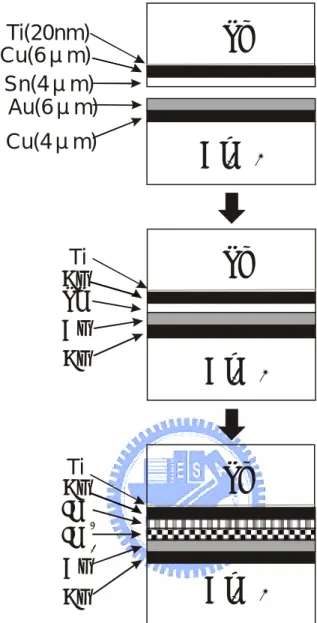
Ever since IBM first started research on copper interconnection technology, [43-45] copper metallization has drawn considerable attention in the IC industry. For the diffusion soldering of Si with Al2O3 substrates, Ti (20 nm), Cu (6 µm) and Sn (4 µm)
were sputter-deposited sequentially on a Si wafer. A Cu layer (4 µm) and an Au layer (6 µm) were also deposited on an Al2O3 substrate by sputtering. The specimens with
dimensions of 4 mm x 4 mm were cut with a diamond saw. The surfaces of the specimens were stripped with a deoxidized agent prior to diffusion soldering in order to remove any oxide film. The multi-layer thin-film specimens were then sandwiched as shown in Fig. 3-1, and heated at various temperatures ranging from 250°C to 400°C in a vacuum furnace of 5.3 x 10⁻⁴ Pa. After diffusion soldering, the specimens were cross-sectioned, ground with SiC paper, and polished with 1 µm and 0.3 µm Al2O3
powders. Morphology observations and growth rate measurements of the intermetallic compounds were mostly conducted via a scanning electron microscope (SEM). Chemical compositions of the intermetallic compounds were analyzed using an electron probe microanalyzer (EPMA). For the evaluation of bonding strengths of the diffusion-soldered specimens, tensile tests were conducted using a microforce tester at a
crosshead speed of 0.01 mm/s.
Fig. 3.1:The scheme of diffusion soldering for Cu/Ti/Si and Au/Cu/Al2O3 with Sn interlayers.
3-2 Experimental Method for Electroless Copper/Nickel Films Deposited
on AlN Substrates
3-2.1 Metallization of AlN substrates
Pretreatments of the surface of nonmetal substrates including roughening, sensitization, activation, and acceleration are necessary before electroless plating. [46-48]
Si
Al
2O
3Cu(6μm)
Sn(4μm)
Au(6μm)
Cu(4μm)
Si
Cu
Sn
Au
Cu
Si
Cu
Au
Cu
IM
1IM
2Al
2O
3Al
2O
3Ti(20nm)
Ti
Ti
Polished and unpolished AlN substrates provided by Stellar Industries were used in this work. Figure 3.2 shows the process flow of pretreatments and the metallization of AlN substrates. Firstly, the substrates were soaked in acetone and ultrasonically cleaned for 5 min to remove the contaminants and then etched in 4 wt% NaOH solution for 30 min. The substrates were further ultrasonically cleaned in deionized water to remove the solution residues, and then dried with helium gas. The surface roughness was evaluated using a surface profiler (KLA-Tencor P-10) and an atomic force microscope (AFM, Digital Instruments Nanoscope Ⅱ).
Fig. 3.2 Process flow of AlN substrate metallization [46-48].
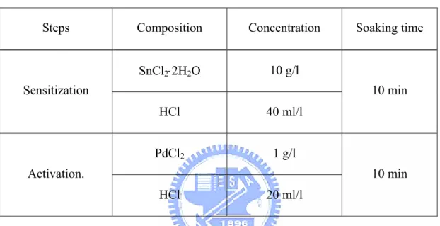
The cleaned AlN substrates were then sensitized and activated with the solutions listed in Table 3.1. The EN plating was followed using the solution consisting of 132 ml/l
A
A
l
l
N
N
(
(
p
p
o
o
l
l
i
i
s
s
h
h
e
e
d
d
/
/
u
u
n
n
p
p
o
o
l
l
i
i
s
s
h
h
e
e
d
d
)
)
s
s
u
u
b
b
s
s
t
t
r
r
a
a
t
t
e
e
S
S
u
u
b
b
s
s
t
t
r
r
a
a
t
t
e
e
p
p
r
r
e
e
-
-
c
c
l
l
e
e
a
a
n
n
(
(
A
A
c
c
e
e
t
t
o
o
n
n
e
e
)
)
R
R
o
o
u
u
g
g
h
h
e
e
n
n
i
i
n
n
g
g
(
(
3
3
0
0
,
,
6
6
0
0
,
,
1
1
2
2
0
0
m
m
i
i
n
n
)
)
/
/
S
S
e
e
n
n
s
s
i
i
t
t
i
i
z
z
a
a
t
t
i
i
o
o
n
n
/
/
A
A
c
c
t
t
i
i
v
v
a
a
t
t
i
i
o
o
n
n
E
E
l
l
e
e
c
c
t
t
r
r
o
o
l
l
e
e
s
s
s
s
N
N
i
i
(
(
P
P
)
)
、
、
C
C
u
u
p
p
l
l
a
a
t
t
i
i
n
n
g
g
/
/
P
P
h
h
o
o
t
t
o
o
l
l
i
i
t
t
h
h
o
o
g
g
r
r
a
a
p
p
h
h
y
y
/
/
e
e
t
t
c
c
h
h
P Pu
u
l
l
l
l
-
-
o
o
f
f
f
f
a
a
n
n
d
d
s
s
h
h
e
e
a
a
r
r
t
t
e
e
s
s
t
t
/
/
R
R
e
e
s
s
i
i
s
s
t
t
a
a
n
n
c
c
e
e
m
m
e
e
a
a
s
s
u
u
r
r
e
e
m
m
e
e
n
n
t
t
/
/
B
B
o
o
n
n
d
d
i
i
n
n
g
g
/
/
A
A
n
n
n
n
e
e
a
a
l
l
i
i
n
n
g
g
(250°C,1
、
2hr)
/
/
Structure(AFM、P-10 、
XRD), Morphology(SEM) and Composition analyses
(SIMS 、EDS)
Slotonip 33 Ni solution, 0.8 ml/l (40%) Slotonip 36 stabilizer, 177 ml/l Slotonip 31 hypophosphite complexing agent and 690.2 ml/l DI water. The deposition was carried out at a temperature of 90°C and the pH of the solution was kept at 4.5. The deposition rate of the EN layer was approximately 21 µm/h.
Table 3.1. Compositions of sensitization and activation solution.
Steps Composition Concentration Soaking time
SnCl2⋅2H2O 10 g/l Sensitization HCl 40 ml/l 10 min PdCl2 1 g/l Activation. HCl 20 ml/l 10 min
The electroless Cu plating solution consisted of MACuShield 185A Cu solution, MACuShield 185B chelating agent, MACuShield 185D modifying agent, MACuShield 185G stabilizer and 37% formaldehyde reducer. During the deposition, the pH value was adjusted in the range of 12 to 13. The Cu layer deposition rate was approximately 4 µm/h.
3-2.2 Surface morphology and composition characterization
The metallized AlN substrates were observed using a Hitachi S-2500 scanning electron microscope and FEI FIB-200 focused-ion-beam (FIB) system. The composition of the Ni layers was analyzed with an energy-dispersive spectrometer attached to the
scanning electron microscope as well as with a PHI Adept 1010 quadrupole secondary-ion-mass spectrometer. The crystal structure of deposited films was characterized by X-ray diffraction analysis (Siemens D-5000).
3-2.3 Pull-off test
A pull-off test was employed to measure the adhesion strength of the EN layer on AlN substrates. Studs of 2.54 mm diameter were firmly attached onto the specimens using epoxy resin and then sent to a SeBastian Five-A pull-off tester for adhesion measurement.
3-2.4 Shear test
Ni bumps of 100 µm in diameter and 30 µm in height were formed on the AlN substrate. The shear test was carried out with a DAGE 2400 shear tester.
3-2.5 Resistance measurement
The sheet resistance (Rs) of the plated metal layer was measured using Changmin
Tech’s CMT-SR 2000N four-point probe. The resistivity (ρ) of the metal layer was calculated according to the formula below within the known film thickness (t).
3-2.6 Flip chip bonding
Eutectic lead-tin (37Pb/63Sn) solder was used to bond chips on substrates for electrical connection. The metallization on the pad of the chip was Cu/TiW/GaAs and that on the substrates was Cu(2µm)/Ni(5µm)/AlN. The apparatus for flip chip bonding was a semiautomatic flip chip bonder (Suss FC 150) with a 1µm bonding accuracy. The solder bumps were grown on GaAs PHEMT devices. The bumped ICs were then bonded onto the metallized AlN substrates prepared according to a previously described method. The specimens were annealed at 250°C for various times and the microstructure evolution of the bonding interface was evaluated by scanning electron microscope (SEM)/ energy-dispersive spectrometer (EDS).
3-3 Experimental Method for Electroless Cobalt-Phosphorous Layer and
Its Diffusion Barrier Properties of Pb-Sn Solder
3-3.1. Specimen Preparation
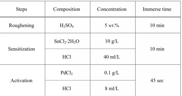
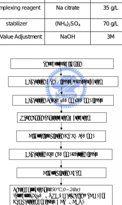
After forming simulated Ti/Cu circuit layer on the Si substrate by e-beam evaporation and then processed by roughening/sensitization/activation, the specimens were subjected to electroless plating of different periods of times for depositing Co(P) layer. Table 3.2 lists the methods and solutions for roughening, sensitization and activation. After the catalytic layer being formed on specimens, a Co(P) layer was deposited thereon by means of the
electroless plating solution defined by Table 3.3, the pH of which was regulated by 3M NaOH. In this experiment, the plating condition was controlled as follows: pH value = 7.8±0.3, temperature = 75±2°C, V/A (ml/cm2) ≥ 20 while the plating time was adjustable
with respect to the required thickness. A surface profiler (KLA-TENCOR P-10) measured the thickness of Co(P) layer on substrates subjected to different plating time, and the plating rate was obtained. After the specimens were washed by DI water and then blew dry by a nitrogen jet, a Cu wetting layer of 800 nm and eutectic PbSn solder layer were sequentially deposited on. The PbSn/Cu/Co(P)/Cu/Ti/Si specimens were then sent to a furnace for annealing at 250°C in forming gas ambient (5% H2-95% N2) for 0, 0.5, 6, 18,
24 hrs, respectively. The flow of specimen preparation is summarized in Fig. 3.3.
Table 3.2. Solution for roughening, sensitization, activation and the immerse time.
Steps Composition Concentration Immerse time
Roughening H2SO4 5 wt.% 10 min SnCl2⋅2H2O 10 g/L Sensitization HCl 40 ml/L 10 min PdCl2 0.1 g/L Activation HCl 8 ml/L 45 sec
Table 3.3. Compositions of electroless plating bath.
Fig. 3.3 Flow chart of Co(P) specimen preparation.
3
3
M
M
N
N
a
a
O
O
H
H
p
p
H
H
V
V
a
a
l
l
u
u
e
e
A
A
d
d
j
j
u
u
s
s
t
t
m
m
e
e
n
n
t
t
7
7
0
0
g
g
/
/
L
L
3
3
5
5
g
g
/
/
L
L
4
4
0
0
g
g
/
/
L
L
3
3
5
5
g
g
/
/
L
L
C
C
o
o
n
n
c
c
e
e
n
n
t
t
r
r
a
a
t
t
i
i
o
o
n
n
(
(
N
N
H
H
44)
)
22S
S
O
O
44N
N
a
a
c
c
i
i
t
t
r
r
a
a
t
t
e
e
N
N
a
a
H
H
22P
P
O
O
22•
•
H
H
22O
O
C
C
o
o
S
S
O
O
44•
•
6
6
H
H
22O
O
C
C
h
h
e
e
m
m
i
i
c
c
a
a
l
l
stabilizer
complexing reagent
R
R
e
e
d
d
u
u
c
c
i
i
n
n
g
g
A
A
g
g
e
e
n
n
t
t
Co salt
I
I
n
n
g
g
r
r
e
e
d
d
i
i
e
e
n
n
t
t
Si substrate cleaning Electroplating PbSnDepositing Cu (800 nm) wetting layer Electroless plating Co(P) (600 nm) Roughening/Sensitization/Activation
Depositing Ti/Cu (100 nm/500 nm) layer Depositing a SiO2 layer by wet oxidation
Thermal treatment(250°C,0∼24hr)
/Structure(P-10 、XRD), Morphology(SEM) and Composition analyses (AES 、EDX)
3-3.2. Structure, Morphology and Composition Characterization
The crystal structures of electroless Co(P) films were characterized by a x-ray
diffractometer (M18 XHF, MacScience). The source of x-ray was Cu-Kα of 0.154 nm
wavelength operated at 200 mA and 50 kV and the measurement was performed at a scanning rate of 4°/min.
Scanning electron microscopy (SEM, FE-SEM JSM-6500F or FE-SEM Hitachi S-4700) was adopted to examine the morphology and cross-sectional structures of each specimen. The composition analysis was performed using Auger electron spectroscopy (AES, VG350) and energy dispersive spectrometer (EDX, Oxford Inca Energy 300) attached to SEM. Further, the EDX line scan was adopted to analyze the composition change for cross-sectional specimens subjected to different durations of thermal treatment. The line scan start from the Cu layer of the substrate toward the PbSn solder while adopting at least four points of each specimen for analysis so as to obtain the average thereof for further discussion.
Chapter 4 Results and Discussion
4-1 Thin-Film Reactions during Diffusion Soldering of Cu/Ti/Si and
Au/Cu/Al
2O
3with Sn Interlayers
The multi-layer thin-film systems of Cu/Ti/Si and Au/Cu/Al2O3 were bonded with
Sn interlayers at various temperatures ranging from 250°C to 400°C. The typical
morphology of the diffusion-soldered joints for the bonding of Cu/Ti/Si and Au/Cu/Al2O3
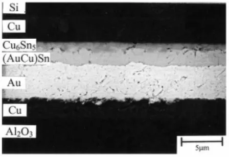
with Sn interlayers is shown in Fig. 4.1. EPMA line profiles for Au, Sn, and Cu elements across the multi-layers of the diffusion-soldered specimen (see Fig. 4.1.) are plotted in Fig. 4.2. The Sn interlayer after diffusion soldering is eliminated and replaced by bilayered intermetallic compounds between Cu/Ti/Si and Au/Cu/Al2O3. The intermetallic
compounds adjacent to the Cu layer have a chemical composition (at.%) of Cu:Au:Sn = 54.8:0.2:45.0, i.e., (Cu0.99Au0.01)6Sn5, which corresponds to the η-Cu6Sn5 phase on the
Cu-Sn phase diagram. The η-Cu6Sn5 intermetallic phase has often been reported on in
studies of Cu/Sn interfacial reactions [49]. During the Cu/Sn soldering reactions, η-Cu6Sn5 has been found to react further with Cu to form the ε-Cu3Sn intermetallic
Fig. 4.1:The morphology of intermetallic compounds formed after diffusion soldering
between Cu/Ti/Si and Au/Cu/Al2O3 at 300°C for 20 min with Sn interlayers.
0 20 40 60 80 100 120 140 0 5 10 15 20 x (µm)
c (at.%)
Fig. 4.2:The Au, Sn and Cu concentrations across the multi-layers of the diffusion
soldered specimen (from Fig. 4.1).
Au Sn Cu
The chemical composition of the intermetallic compound adjacent to the Au layer is Au:Cu:Sn = 44.4:6.9:48.7, i.e., (Au0.87Cu0.13)Sn, corresponding to the δ-AuSn phase on
the Au-Sn phase diagram. The relatively high Cu content of this δ-AuSn intermetallic phase is attributed to the rapid diffusion of Cu into the Au layer in Au/Cu/Al2O3, which
simultaneously participates in the interfacial reaction between Au and the Sn interlayer during the diffusion soldering process. For the soldering reaction between liquid Sn and the Au substrate, the interfacial intermetallic compound most commonly formed is the AuSn4 phase [50]. The appearance of the δ-AuSn phase can be attributed to a further
reaction of AuSn4 with the Au layer following the exhaustion of the Sn interlayer.
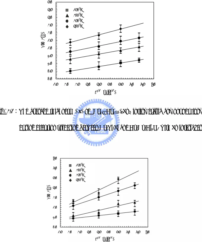
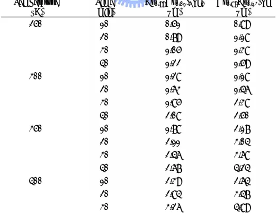
The average thickness (∆x) of the intermetallic layers formed at the interface was measured and listed in Table 4.1. The data are plotted against the square root of reaction time (t) and shown in Figs. 4.3 and 4.4 for the (Cu0.99Au0.01)6Sn5 and (Au0.87Cu0.13)Sn
phases, respectively. In both cases, the growths of intermetallic compounds follow a parabolic rate law, implying that their reactions are diffusion-controlled. The growth rate constants (k = ∆x/t1/2) as calculated from Figs. 4.3 and 4.4 are given in Table 4.2. From
the Arrhenius diagram of lnk vs 1/T as shown in Fig. 4.5, the activation energies (Q) for the growths of (Cu0.99Au0.01)6Sn5 and (Au0.87Cu0.13)Sn intermetallic compounds can be
determined as 16.9 kJ/mol and 53.7 kJ/mol, respectively. The former value (16.9 kJ/mol) is quite consistent with the activation energy for the diffusion of Cu in liquid Sn (19.5 kJ/mol), as reported by Ma and Swalin [51]. It implies that the rate-limiting step in the
growth of the (Cu0.99Au0.01)6Sn5 intermetallic is the diffusion of Cu dissolved near the
intermetallic reaction front into the surrounding liquid Sn thin-film.
0.0 0.5 1.0 1.5 2.0 2.5 3.0 3.5 4.0 4.5 5.0 2.5 3.0 3.5 4.0 4.5 5.0 5.5 6.0 6.5 7.0 t1/2 (min1/2) ∆ x ( µm) 250oC 300oC 350oC 400oC
Fig. 4.3:The average thickness (∆x) of (Cu0.99Au0.01)6Sn5 intermetallic compounds formed
during diffusion soldering between Cu/Ti/Si and Au/Cu/Al2O3 with Sn interlayers.
0.0 1.0 2.0 3.0 4.0 5.0 6.0 7.0 2.5 3.0 3.5 4.0 4.5 5.0 5.5 6.0 6.5 7.0 t1/2 (min1/2) ∆ x (µm) 250oC 300oC 350oC 400oC
Fig. 4.4:The average thickness (∆x) of (Au0.87Cu0.13)Sn intermetallic compounds formed
-2.0 -1.6 -1.2 -0.8 -0.4 0.0 0.4 1.4 1.5 1.6 1.7 1.8 1.9 2.0 1000/T (K-1) ln k (µm/min 1/2 ) Q=53.7 kJ/mol Q=16.9 kJ/mol
Fig. 4.5:The Arrhenius plots of growth rate constants (k) for (Cu0.99Au0.01)6Sn5 and
(Au0.87Cu0.13)Sn intermetallic compounds formed during diffusion soldering between
Cu/Ti/Si and Au/Cu/Al2O3 with Sn interlayers.
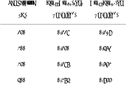
Table 4.1. Thicknesses of intermetallic compounds formed during diffusion soldering between Cu/Ti/Si and Au/Cu/Al2O3 with Sn interlayers.
Temperature (°C) Time (min) (Cu0.99Au0.01)6Sn5 (µm) (Au0.87Cu0.13)Sn (µm) 250 10 0.51 0.89 20 0.79 1.18 30 1.05 1.38 40 1.22 1.59 300 10 1.28 1.18 20 1.63 1.46 30 1.85 2.38 40 2.08 2.50 350 10 1.78 2.17 20 2.11 3.04 30 2.46 3.68 40 2.67 4.24 400 10 2.39 2.64 20 2.84 3.47 30 3.26 4.89 (Au0.87Cu0.13)Sn (Cu0.99Au0.01)6Sn5
Table 4.2. Growth rate constants of intermetallic compounds formed during diffusion
soldering between Cu/Ti/Si and Au/Cu/Al2O3 with Sn interlayers.
Temperature (°C) (Cu0.99Au0.01)6Sn5 (µm/min1/2) (Au0.87Cu0.13)Sn (µm/min1/2) 250 0.228 0.219 300 0.250 0.462 350 0.287 0.653 400 0.374 0.955
Tu and Thompson [52] reported that the growth of Cu6Sn5 intermetallic compound
during the solid-state reaction between Cu and Sn thin films at room temperature exhibited a linear rate. According to their discussion, the rate-limiting step should be the release of Cu atoms from the Cu film, rather than the diffusion across Cu6Sn5. In contrast to the
thin-film reaction discussed by Tu and Thompson, Vianco et al. [53] studied the solid-state interfacial reaction between Cu and hot-dipped Sn at temperatures ranging from 70℃ to 205℃. Parabolic growth kinetics for Cu6Sn5 intermetallic compounds was reported.
The deviation of the reaction mechanism in Tu and Thompson’s study [52] from the
research of Vianco et al. [53], should be attributed to the ultra-thin film specimens (Sn thickness under 0.5 µm) and the quite low reaction temperature (room temperature) adopted by the former study. For the solid-liquid interdiffusion between Cu and Sn thin
films at 240℃ and 300℃, Bader et al. showed that the growth of Cu6Sn5 intermetallic
compound did not follow the parabolic growth law [8]. As was explained by them, the deviation was attributed to the reduction of transport grooves resulting from the growth of the scallop-shaped Cu6Sn5 intermetallic compounds. Since the kinetic measurements
obtained by Bader et al. were focused on the initial stage of reaction (reaction time: shorter than 2 mins; intermetallic thickness: thinner than 2µm), it is believed that once all the grooves along the interface have “closed” after a longer reaction time as similar for our study (reaction time: 10 mins to 40 mins), the reaction-controlling step in the growth of Cu6Sn5 should turn out to be the diffusion through the continuous Cu6Sn5 intermetallic
layer. Hayashi et al. [54] studied the soldering reactions between Cu and liquid Sn saturated with Cu, and found that the growth of Cu6Sn5 intermetallic compound was
diffusion-controlled with an activation energy of 29 kJ/mol, a value quite near our own kinetic measurement (16.9 kJ/mol). In summery of the above results, it can be implied that the solid-liquid interfacial reactions in the Cu/Sn thin film case are carried out similarly to a “normal” soldering reaction.
The calculated activation energy for the growth of the (Au0.87Cu0.13)Sn intermetallic
(53.7 kJ/mol) is close to the activation energy for the lattice diffusion of Au in Sn (║C:
46.1 kJ/mol, ⊥ C: 74.1 kJ/mol), as reported by Dyson [55]. The growth of the
(Au0.87Cu0.13)Sn intermetallic is, therefore, believed to be controlled by the lattice
rate-controlling mechanisms for (Cu0.99Au0.01)6Sn5 and (Au0.87Cu0.13)Sn intermetallics may
be attributed to the much quicker liquid/solid reaction for Sn(l)/Au(s) than that for Sn(l)/Cu(s).
This explanation can be validated by the quite different wettability of liquid Sn on Au and Cu substrates. Figure4.6 shows that the contact angle of liquid Sn on the Au substrate decreases rapidly and vanishes at complete wetting (~0°), while the contact angle in the case of the Cu substrate remains at about 30°, implying that it is much easier for liquid Sn to react with Au than with Cu. In other words, Au0.87Cu0.13 reacts rapidly during
diffusion-soldering with Sn to form (Au0.87Cu0.13)Sn4. After the thin-film Sn is exhausted,
a further solid/solid interfacial reaction takes place: (Au0.87Cu0.13)Sn4 + 3(Au0.87Cu0.13) →
4(Au0.87Cu0.13)Sn. Since the reaction efficiency is governed by the slow mode of the
latter reaction, the rate-controlling mechanism for the growth of (Au0.87Cu0.13)Sn is
therefore the diffusion of Au in this solid intermetallic phase. The solid/solid interfacial reaction in the Au/Pb-Sn solder system has been studied by Hannech and Hall [56]. They found that an AuSn4 intermetallic compound was formed under diffusion control during
reaction. The activation energy was 40 kJ/mol, similar to the value of our measurement for the solid/liquid thin film reaction of the Au/Sn system (53.7 kJ/mol). Their results sustain the view held by this present study, that the growth of (Au0.87Cu0.13)Sn is
controlled by a solid/solid interfacial reaction as discussed previously.
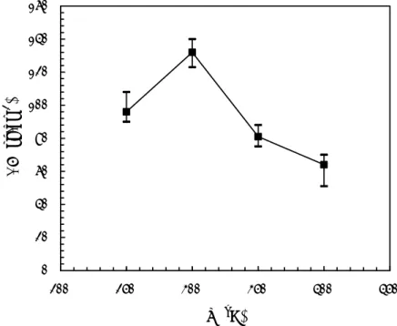
Tensile strengths of the specimens after diffusion soldering at various temperatures for 20 min are shown in Fig. 4.7. A maximum value of 132 kg/cm2 is attained at the
bonding temperature of 300°C. As Table 4.1 indicates, such an optimized bonding condition (300°C, 20min) is conducive to the growth of (Cu0.99Au0.01)6Sn5 and
(Au0.87Cu0.13)Sn intermetallic layers to the thicknesses of 1.63 µm and 1.46 µm,
respectively. This thesis proposed a novel joining technique using diffusion soldering technique for die attachment to bond different materials, which has less defects at bonding parts such as coagulation cracks or gas cavities.
0 10 20 30 40 50 60 70 80 90 100 0 20 40 60 80 100 120 t (time) θ (degree) Sn/Au Sn/Cu
Fig. 4.6:The contact angles (θ) of liquid Sn on the surfaces of Au and Cu substrates at
0 20 40 60 80 100 120 140 160 200 250 300 350 400 450 T (oC) ∆σ (kg/cm 2 )
Fig. 4.7:The tensile strengths (σ) of Cu/Ti/Si wafer diffusion-soldered with Au/Cu/Al2O3
substrates at various temperatures for 20 min using an Sn thin-film interlayer.
4-2 Electroless Copper/Nickel Films Deposited on AlN Substrates
4-2.1 Surface morphology of AlN substrates
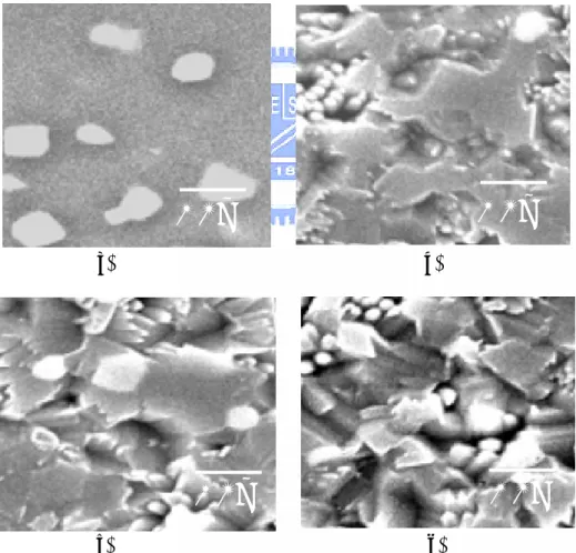
Figure 4.8 is a SEM image of the polished AlN substrate surface. After being etched by the NaOH solution, the surface became rougher and rougher with increasing etching time. The white granules in Fig. 4.8(a) should be the Al-Y-O compounds reported in previous studies. [57,58] Figure 4.9 shows the SEM image of the unpolished substrate surface in which AlN grains are clearly visible. The etching removed the small grains, and with increasing etching time, various column-like holes were generated. Figure 4.10 shows the variation in AlN surface roughness with etching times measured by atom force microscopy
(AFM). As shown in Fig. 4.10, the roughness of unpolished AlN substrates is always higher than that of polished AlN substrates regardless of the duration of etching time. Furthermore, the roughness of the polished AlN substrate increases with increasing etching time, while the roughness of the unpolished AlN surface reaches a peak value of 0.45 µm after 60 min etching and further etching does not seem to exacerbate the roughness. We believe that the etched, unpolished AlN substrates should possess a higher roughness since the tip of the AFM probe might not be able to reach the bottom of the holes on the sample surface hence the true surface roughness could not be totally revealed.
(a) (b)
(c) (d)
Fig. 4.8: Surface morphology of polished AlN surface after etching for (a) 0 min, (b)
30 min, (c) 60 min, and (d) 120 min
4
µm
4
µm
(a) (b)
(c) (d)
Fig. 4.9: Surface morphology of unpolished AlN surface after etching for (a) 0 min,
(b) 30 min, (c) 60 min, and (d) 120 min.
Fig.4.10: Variation in AlN surface roughness with etching time.
4μm
4
µm
4
µm
4
µm
4μm
4
µm
0
20
40
60
80
100
120
0.0
0.1
0.2
0.3
0.4
0.5
0.6
0.7
Surface roughness (
µm)
Time (min)
Polished
Unpolished
(a) (b)
(c) (d)
Fig.4.11: Surface morphologies of electroless Ni plated on polished AlN substrates for
(a) 0.5 min, (b) 1 min, (c) 4.5 min, and (d) 26.5 min.
4-2.2 Surface morphology of electroless-plated metal layers
Figures 4.11 and 4.12 show the surface morphologies of the EN plated on polished and unpolished AlN substrates etched for 30 min, respectively. It can be clearly seen that the EN films plated on the polished surface possess a finer grain structure than those on the unpolished surface, however, the EN films on the unpolished substrate are rugged and
1
µm
1
µm
1
µm
void-embedded. In both types of AlN substrates, the Ni grains should initiate from the Pd seeds formed during the surface activation. On the polished AlN substrate, the Ni granules grew and soon coalesced with each other to form the fine grain structure as shown in Fig. 4.11 [see illustration in Fig. 4.13(a)]. On the unpolished AlN substrate, even though the rougher surface might offer more nucleation sites as predicted by the heterogeneous nucleation theory, our experimental observation indicated that this could not be applied to electroless plating of the unpolished AlN substrate. As shown in Fig. 4.14(b), cross-sectional view of the Ni/AlN interface reveals that in fact the Ni does not fill up the etched holes in an unpolished AlN substrate. Probably the capillarity effects prevented the activation solution from reaching the bottom of the holes that metallization could only proceed on the top region of the unpolished surface [see illustration in Fig. 4.13(b)]. Another possible cause of this was the gaseous bubbles generated during plating, which inhibited the full coverage of metallization. Since the Ni granules located at the tops of the column-like grains must grow to a certain size to coalescence with each other, the Ni layer thus exhibits a coarse grain structure as shown in Fig. 4.12. Furthermore, if the coalescence fails, voids form in the Ni layer, as shown in Fig. 4.12(d).
(a) (b)
(c) (d)
Fig.4.12:Surface morphologies of electroless Ni plated on unpolished AlN
substrates for (a) 0.5 min, (b) 1 min, (c) 4 min, and (d) 30 min.
(a)
(b)
Fig. 4.13: Illustration of grain growth on (a) polished and (b) unpolished AlN substrates.
1
µm
2
µm
8
µm
1
µm
AlN
AlN
Nuclei
Nuclei
Ni
Ni
(a)
(b)
Fig. 4.14: Cross-sectional view of EN layer plated for 3 min on (a) polished and (b)
unpolished AlN substrates.
(a) (b)
Fig. 4.15: Surface morphologies of electroless Cu plated on (a) polished and (b)
unpolished AlN substrates plating for 90 min.
Figures 4.15(a) and 4.15(b) show the surface morphologies of the electroless Cu plated on polished and unpolished AlN substrates, respectively. The differences in surface
AlN
8
µm
8
µm
roughness and grain size clearly indicate that the surface roughness of the AlN substrate affects the morphology of the subsequently plated film. The flat AlN substrate can generate a flat Cu layer with a fine grain structure.
4-2.3 Resistivity measurement
Figures 4.16(a) and 4.16(b) depict the resistivities of Ni and Cu layers on the polished and unpolished AlN substrates, respectively. In both cases, the resistivities of deposited films on the polished AlN surface are always lower than those on the unpolished AlN surface. Apparently, the rougher, unpolished AlN substrate surface induced defects in the film interface during grain clustering and thereby deteriorated the electrical conductivity of the deposited layers.
The specimens were also annealed at 250°C for 1 h under inert ambient. Even though a decrease in resistivity was observed, subsequent XRD analysis revealed that no marked structure change occurred in the deposited layers. The decrease in resistivity might be a result of the annihilation of point defects and dislocations, rather than of the recrystallization and grain growth phenomena in the Ni and Cu layers. There was no obvious change in the microstructures of metal films subjected to a 250°C˘1 h annealing.
(a)
(b)
Fig. 4.16: Resistivities of electroless (a) Ni and (b) Cu deposited on polished and
4-2.4 Structure and composition analyses of plated Ni and Cu layers
The amorphous feature of EN films indicates that they are in a non-equilibrium state.
[57] Figures 4.17(a) and 4.17(b) show the XRD patterns of EN films before and after
250°C˘1 h annealing. It can be seen that the thin EN film was amorphous and, with the increase in plating time, the crystallinity of the EN film gradually improved. Nevertheless, the EN film plated over 15 min (or film thickness > 5µm) still has a wide peak distributed over the diffracted angle range of 37° to 55°. This is due to the fact that during plating, the phosphorus atoms were incorporated in the Ni deposition reducing its crystallization. Figures 4.17(a) and 4.17(b) further indicate that the structure of the EN films did not change markedly with the 250°C˘1 h annealing. Figures 4.18(a) and 4.18(b) show the XRD patterns of Cu films before and after the 250°C˘1 h annealing. The Cu films were polycrystalline, evidenced by the sharp (111) and (200) diffraction peaks appearing at 43.3° and 50.4°, respectively.
(a)
(b)
Fig. 4.17 XRD pattern of Ni/AlN (a) before and (b) after 250°C 1 h annealing ( : AlN; :Ni)
30
40
50
60
70
(103)
(110)
(102)
(111)
(101)
(002)
(100)
30 15 6 3Intensity
2θ (°)
Ni_3min
Ni_6min
Ni_15min
Ni_30min
30
40
50
60
70
(103)
(110)
(102)
(111)
(101)
(002)
(100)
3 6 15 30Intensity
2θ (°)
Ni_3 min
Ni_6 min
Ni_15 min
Ni_30 min
(a)
(b)
Fig. 4.18: XRD pattern of Cu/Ni/AlN (a) before and (b) after 250°C˘1 h annealing.
( : AlN; :Cu)