國 立 交 通 大 學
電機與控制工程學系
碩 士 論 文
應用於初次側調整控制器之高效率及低成本
膝點電壓追蹤調整技術
Primary-Side Regulator with Self-Calibration Knee Voltage Detection
(KVD) Technique for High Efficiency and Low Cost
研 究 生:葉之樸
指導教授:胡竹生 博士
陳科宏 博士
用於初次側調整控制器之高效率及低成本膝點電壓追蹤調整技術
Primary-Side Regulator with Self-Calibration Knee Voltage Detection
(KVD) Technique for High Efficiency and Low Cost
研 究 生:葉之樸 Student:Chih-Pu Yeh
指導教授:胡竹生 Advisor:Jwu-Sheng Hu
陳科宏 Advisor:Ke-Horng Chen
國 立 交 通 大 學
電 機 與 控 制 工 程 學 系
碩 士 論 文
A Thesis
Submitted to Department of Electrical Control Engineering
College of Electrical Engineering
National Chiao Tung University
in partial Fulfillment of the Requirements
for the Degree of
Master
in
Electrical Control Engineering
November 2012
Hsinchu, Taiwan, Republic of China
用於初次側調整控制器之高效率及低成本膝點電壓追蹤調整技術
研究生:葉之樸
指導教授:胡竹生博士 陳科宏博士
國立交通大學電機與控制工程研究所碩士班
摘 要
在現今社會,可攜式產品已經成為人人不可或缺的必備工具。隨著電子產品的蓬勃 發展,可充電電池也成為目前最適合可攜式產品使用的行動電源。因此,如何以最理想 且安全的方式將能量傳遞到電池,對電池進行最快速也最有效率的充電是一個重要的課 題。基於通用串行總線充電變成一種趨勢,從交流市電直接對電子產品充電是現在大部 分可攜式產品的充電方式。初次側調整控制器是一種高效率而且低成本的充電器,同時 也是一種能容忍市電的高輸入電壓隔離式充電器。為了確保充電器在定電流充電模式與 定電壓充電模式皆能保持穩定且平穩切換,本切換式充電器將定電流充電迴路與定電壓 充電迴路並聯,且同時達到兩者的穩定性。但是初次側調整控制器與一般控制器最大的 分別就是它並沒有直接的迴授路徑來獲取輸出資訊,因此如何準確從輔助繞組中去取得 膝點電壓進而去控制整個系統變成一個重要問題。 本篇論文完成一具有膝點電壓偵測電路,同時針對偵測的時間做自我的調整來避免 發生偵測錯誤。不同於以往的方式,這次提出的偵測電路不僅能準確的偵測膝點電壓, 並不需要外部原件來做修正,同時也使所有的控制路徑在定電流充電模式與定電壓充電 模式皆能保持穩定且平穩切換。為了使效率更進一步提升,波谷切換以及動態頻率切換 被應用在定電壓充電模式。Primary-Side Regulator with Self-Calibration Knee Voltage Detection (KVD)
Technique for High Efficiency and Low Cost
Student: Chih-Pu Yeh
Advisor: Dr. Jwu-Sheng Hu & Dr. Ke-Horng Chen
Department of Electrical Control Engineering
National Chiao-Tung University
Abstract
Nowadays portable devices have been considered a necessity by a lot of people and have
become an essential part of everyday life. With the rapid growth in the consumer electronics,
rechargeable mobile battery bank has proved to be the most compatible and satisfactory
solution for portable devices. Therefore, it will be an important task for us to create a fast and
efficient battery charging method with safe delivery of energy to the battery. Since universal
serial bus (USB) charging method is a common trend now, most of the portable devices are
charged via alternating current (AC) supply combine with USB. Primary-side regulator (PSR)
is a high efficiency and low cost solution for power applications. It is a high-input voltage
isolated charger compatible with the AC supply. To stabilize and to smoothly transit between
the constant voltage and the constant current modes, the constant voltage and constant current
loops are connected in parallel in the proposed PSR charger. However, the prominent
difference between the PSR and conventional regulators is that the PSR does not have direct
feedback loop to obtain the output information. Hence, it is a major challenge to precisely
detect knee voltage from the auxiliary winding and thus to accurately control the entire
system.
technique, which it can perform self-calibration based on the detection period for error
checking and correction. Moreover, the new detection method not only can precisely get the
knee voltage without any external components, but also can have all control paths stabilized.
The transition smoothly changes between the constant voltage and the constant current modes.
Valley switching with a dynamic frequency switching is applied in the constant voltage mode
誌 謝
兩年多來的碩士班生涯,要感謝許多的人在這一路上對我的幫助。首先要感謝我的 家人一直不斷的支持及照顧我。包括我的爸爸媽媽,還有露露,感謝你們長久的陪伴和 督促,才能讓生性偷懶的我一直支撐下去。 首先要感謝我的指導教授陳科宏博士,您幽默風趣的談吐、不厭其煩的教導、與我 們亦師亦友、共同進退的形象,會是最棒的回憶。更感謝您對此篇論文不厭其煩的修改 與修正,真的是辛苦您了。除此之外,提供豐富的研究資源、充分給予挑戰嘗試的機會, 並提供生活關心照顧,更是我學習成長的一大動力。 感謝實驗室學長們在研究生活中的照顧。感謝昱輝學長、期哥學長、斤哥學長、小 契學長、小蔡學長、昭彰學長、暐中學長、蘇蘇學姊、雅萍學姐、怡婷學姐。感謝有你 們在學業上與生活上的照顧與指導。 感謝同儕阿倪、垮克、GM、大龍。能夠與你們成為夥伴一起討論切磋、互相勉勵、 共度實驗室生活,真的很開心。謝謝阿倪與 GM,你們是所有人之中我最能夠在修課中依 賴的人,感謝你們不時地提醒我上課的資訊,以及督促我上課的內容,你們的努力絕對 會在往後的日子給你的回報,希望你們日後都能飛黃騰達。感謝垮克與大龍,你們是我 在實驗室中能夠陪我聊天講垃圾話的夥伴,有你們在的日子中,實驗室變得開心許多, 希望你們都可以找到你們的目標,做你們真正想做的事,也希望大家以後可以多聚聚。 感謝各位學弟,澎澎、亞當、祖為、pony、紹祥、浩子,實驗室有你們變的更活潑 有朝氣。感謝澎澎、祖為、亞當以及紹祥,謝謝你們的陪伴與討論,也謝謝你們在娛樂 方面的切磋以及指教,也感謝助理巧潔平時的幫忙。同時也感謝五年碩的學弟們,感謝 你們為實驗室帶來了許多了歡樂。 最後我要特別感謝我的最愛露露,感謝你一路陪伴我,陪我來到了新竹。感謝你雖 然辛苦,但都盡力滿足我的一切。跟你一起在新竹的這 2 年給了我很多成長,也讓我在 課業之餘,能過得非常充實,也謝謝你的不離不棄,以及你們家人的包容與幫助。僅以此論文獻給我愛的人及愛我的人,家人們、同學們、朋友們和所有關心我的人。 因為有你們,使本論文豐富不少,謝謝你們。
之樸 于 小雪 國立交通大學 中華民國一百零一年十一月
Contents
CHAPTER 1 ... 1
INTRODUCTION ... 1
1.1 THE BASIC CONCEPT OF THE ISOLATED CONVERTER ... 3
1.1.1 Architecture of Asymmetrical Isolated Converters ... 5
1.1.2 Architecture of Symmetrical Isolated Converters ... 8
1.2 MOTIVATION ... 12
1.3 THESIS ORGANIZATION ... 13
CHAPTER 2 ... 14
BASIC DEFINITION PRINCIPLES OF FLYBACK CONVERTERS ... 14
2.1 THE BASIC OPERATION OF FLYBACK CONVERTER ... 15
2.2 NON-IDEAL PHENOMENON OF FLYBACK CONVERTER IN DCM ... 18
2.3 LOSSES AND EFFICIENCY ANALYSIS ... 20
2.3.1 Conduction Loss ... 21
2.3.2 Switching Loss ... 21
2.3.3 Quiescent Loss ... 22
2.3.4 Efficiency ... 23
CHAPTER 3 ... 24
THE PROPOSED PRIMARY-SIDE REGULATOR WITH SELF-CALIBRATION KNEE VOLTAGE DETECTION (KVD) TECHNIQUE ... 24
3.1 SIGNIFICANT ADVANTAGES OF PSR FLYBACK CONVERTER COMPARED TO CONVENTIONAL DESIGN ... 24
3.2 THE CONVENTIONAL CONTROL OF PSR ... 26
3.3 THE PROPOSED CHARGER BY THE PSR CONTROLLER WITH THE KVD TECHNIQUE ... 30
CHAPTER 4 ... 40
4.1 THE CURRENT CALCULATOR ... 40
4.2 THE IMPLEMENTATION OF KNEE VOLTAGE DETECTOR ... 42
4.3 THE IMPLEMENTATION OF SELF-CALIBRATOR ... 45
4.4 THE STABILITY OF THE SYSTEM ... 48
CHAPTER 5 ... 51
SIMULATION RESULTS, ... 51
5.1 SIMULATION RESULTS ... 52
5.2 COMPARISON WITH THE PRIOR ARTS ... 57
CHAPTER 6 ... 59
CONCLUSIONS AND FUTURE WORKS ... 59
6.1 CONCLUSIONS ... 59
6.2 FUTURE WORKS ... 59
FIGURE CAPTIONS
Fig. 1. Isolated power topologies with complexity and efficiency ... 4
Fig. 2. Flyback converter. ... 6
Fig. 3. Forward converter. ... 7
Fig. 4. Push-pull converter. ... 9
Fig. 5. Half-bridge converter. ... 10
Fig. 6. Full-bridge converter. ... 11
Fig. 7. Flyback converter operates in DCM and CCM. ... 16
Fig. 8. (a) Non-ideal flyback converter. (b) Waveform of flyback converter. ... 20
Fig. 9. Transient waveform of VDS and ID curve in switching losses on power MOSFET. ... 21
Fig. 10. (a) Conventional flyback converter. (b) Flyback converter with the PSR controller. . 25
Fig. 11. (a) Operation of the PSR power stage. (b) Knee voltage reveals the VO information. 27 Fig. 12. (a) Sampling pulse generator. (b) Sampling pulse with different expected voltage’s operation. ... 28
Fig. 13. (a) Adjust circuit. (b) Different regulation reference. ... 29
Fig. 14. The S/H of knee point according to VDET and VDELAY. ... 30
Fig. 15. Proposed PSR controller. ... 32
Fig. 16. Constant Current Operation in the PSR controller. ... 32
Fig. 17. Constant voltage operation in the PSR controller. ... 33
Fig. 18. The definition of CC/CV operation with output current/voltage. ... 35
Fig. 19. The transition from the CC operation to the CV operation. ... 36
Fig. 20. (a) The operation of the dynamic frequency technique. (b) The switching frequency versus the output current. (c) The slight variation of the switching frequency if one of the valley voltages is selected... 39
Fig. 21. (a) The current calculator circuit. (b) The timing diagrams. ... 41
Fig. 22. (a) The KVD circuit. (b) Timing diagrams of the KVD technique. ... 43
Fig. 23. The circuit of subtractor. ... 44
Fig. 24. Flow chart with state machine of Self-Calibrator. ... 46
Fig. 25. (a) Self-calibrator circuit. (b) Waveforms in different Mode. ... 47
Fig. 26. Up/down counter. ... 47
Fig. 27. (a) Equivalent small signal model of the proposed PSR in CV regulation. (b) Waveforms of the dynamic frequency technique. ... 50
Fig. 28. Chip micrograph. ... 51
Fig. 29. Simulation results of the PSR operation in the DCM. ... 53
Fig. 30. Simulation results of the current calculator. ... 53
Fig. 31. Simulation results of the KVD technique. ... 54
Fig. 32. (a) Self-Calibrator in Mode 2 to Mode 4 (b) Self-Calibrator form Mode 2 to Mode 3. ... 55
Fig. 33. (a) PSR Operation Changing from CC to CV. (b) Dynamic Frequency in CV Regulation. ... 56
Fig. 34. Charging Sequence of PSR. ... 57
Table Captions
TABLE I Different types of isolated converters. ... 4 TABLE II Comparison of flyback converter operating at CCM and DCM ... 17 TABLE III Design Specifications ... 51
Chapter 1
Introduction
The isolated architecture is widely used in nowadays power system because of it has
many advantages. Such as it is quite safety and convince to design in wide range voltage
difference situation between output and input voltage. Flyback [1] converter is one of isolated
converter [2]. Unlike the conventional power system, isolated converter uses a pair of coils to
transmit electric power via magnetic coupling. It protects the back-end device from high input
voltage through the isolation from transformer. In view of the portable device become a trend,
one of control methods of flyback called primary-side regulator (PSR) becomes more
important.
Recently, the portable devices like personal digital assistants, smart phones, laptops and
digital cameras etc., have become the most popular applications [3]. Rechargeable batteries
combine universal serial bus (USB) charging method are used in these applications for green
energy and linking devices to personal computer. Also most of the portable devices are
charged via alternating current (AC) supply. PSR is a high efficiency and low cost solution for
these power applications. It is also a high input voltage isolated charger compatible with AC
supply.
The proposed PSR is using the topology of flyback converter and used for battery
charger. Also the self-calibration with knee voltage detection (KVD) technique is proposed to
enhance the accuracy of sensing battery voltage. The improving of the sensing accuracy can
voltage (CV). It can prevent overcharging for battery [4] [5] and improve the efficiency of the
1.1 The Basic Concept of the Isolated Converter
The switching mode charger can be classified according to system topology. The most
important distinction is isolated converters and non-isolated ones. Most of the electrical
equipment needs the isolation for high-voltage safety consideration. The advantages about
isolation such as the separation of direct contact from input to output, and the improved
common-mode voltage rejection from input source. Moreover, there are some standards
defined by different institutions in different countries such as the U.S. specifications (UL,
CSA) and the European specifications (IEC, EN). Every product on the market must be
approved by these institutions.
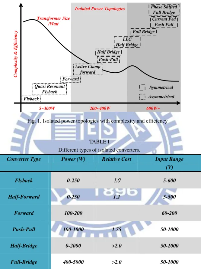
The isolated power converters have many different topologies according to the
application of output watts of electrical device. Fig. 1. shows some common isolated
topologies that apply in different output power. Each topology has different designed
complexity and conversion efficiency. TABLE I shows some different types of isolated
converters and some of its characteristic.
According to the operation of the isolated converter, there are two types of isolated
topologies like asymmetrical and symmetrical. The asymmetrical type uses only one switch to
transfer the energy from primary side to output side through the transformer such as flyback
and forward. And the symmetrical type always uses an even number of switches. Compare to
asymmetrical converters, it is better exploits the transformer’s magnetic circuit than in
asymmetrical converters. So, smaller size and weight can be achieved. In other words, if it
uses the same size of transformer, the symmetrical type could supply more output power. The
Flyback Quasi Resonant Flyback Forward Half Bridge LLC Half Bridge Push-Pull Full Bridge Phase Shifted Full Bridge Current Fed Push Pull Active Clamp forward 5~300W 200~400W 600W~
Isolated Power Topologies
C o m p le x it y & E ff ic ie n cy Transformer Size /Watt Symmetrical Asymmetrical
Fig. 1. Isolated power topologies with complexity and efficiency
TABLE I
Different types of isolated converters.
Converter Type Power (W) Relative Cost Input Range
(V) Flyback 0-250 1.0 5-600 Half-Forward 0-250 1.2 5-500 Forward 100-200 60-200 Push-Pull 100-1000 1.75 50-1000 Half-Bridge 0-2000 >2.0 50-1000 Full-Bridge 400-5000 >2.0 50-1000
1.1.1 Architecture of
Asymmetrical Isolated
Converters
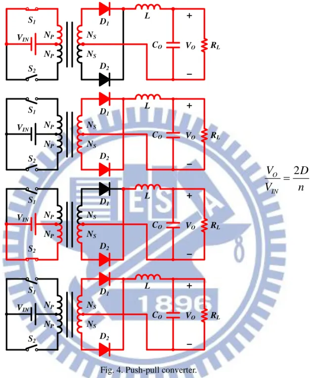
One of the most common asymmetrical isolated converters is flyback converter. The
flyback converter is used in both AC/DC and DC/DC conversion with galvanic isolation
between the input and any outputs. More precisely, the flyback converter is a buck-boost
converter with the inductor split to form a transformer, so that the voltage ratios are multiplied
with an additional advantage of isolation. When driving for example a plasma lamp or a
voltage multiplier the rectifying diode of the buck-boost converter is left out and the device is
called a flyback transformer.
Fig. 2 shows the structure of flyback converter [6]. When the switch is closed, the
primary of the transformer is directly connected to the input voltage source. The primary
current and magnetic flux in the transformer is increasing, and storing energy in the
transformer. The voltage induced in the secondary winding is negative, so the diode is
reverse-biased (i.e., blocked). When the switch is opened, the primary current and magnetic
flux drops. The secondary voltage is positive, forward-biasing the diode, allowing current to
flow from the transformer. The energy from the transformer core recharges the capacitor and
supplies the load. The output capacitor supplies energy to the output load. The operation of
storing energy in the transformer before transferring to the output of the converter allows the
topology to easily generate multiple outputs with little additional circuitry, although the output
voltages have to be able to match each other through the turns ratio. Also there is a need for a
controlling rail which has to be loaded before load is applied to the uncontrolled rails, this is
to allow the PWM to open up and supply enough energy to the transformer. If the turns ratio
of the transformer n=NP/NS and D means the duty cycle of on-time, the conversion ratio of
from 5W up to 250W. Flyback topology is dedicated to multiple low cost output switch mode
power supply as there is no filter inductor on the output.
The forward converter as shown in Fig. 3 is a DC/DC converter that uses a transformer
to increase or decrease the output voltage (depending on the transformer ratio) and provide
galvanic isolation for the load [7]. With multiple output windings, it is possible to provide
both higher and lower voltage outputs. It operates in a manner similar to the flyback converter,
but is generally more energy efficient. A flyback converter stores energy as a magnetic field in
an inductor air gap during the time the converter switching element (transistor) is conducting.
When the switch turns off, the stored magnetic field collapses and the energy is transferred to
the output of the flyback converter as electric current. The flyback converter can be viewed as
two inductors sharing a common core. In contrast the forward converter (which is based on a
transformer) does not store energy during the conduction time of the switching element -
transformers cannot store a significant amount of energy unlike inductors. Instead, energy is
passed directly to the output of the forward converter by transformer action during the switch
V
INC
OR
LN
PN
SV
OD
1S
1V
INC
OR
LN
PN
SV
OD
1S
11
1
O INV
D
V
n
D
conduction phase. The demagnetization and primary windings have to be tightly coupled to
reduce the voltage spike more than the theoretical 2Vin occurring at turn-off across the power
switch. Besides, forward regulators are commonly used for output power up to 300W.
VIN CO VO RL NP NS L D3 D1 D2 ND S1 VIN CO VO RL NP NS L D3 D1 D2 ND S1 VIN CO VO RL NP NS L D3 D1 D2 ND S1 O IN
V
D
V
n
1.1.2 Architecture of Symmetrical Isolated
Converters
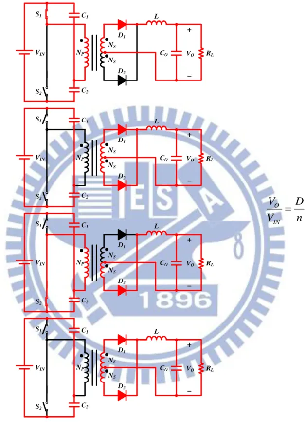
There are three types of symmetrical isolated converters will beintroduced below. Firstly, push-pull has two switches and two diodes as shown in Fig. 4. S1
and S2 switches are alternately turned on. The push–pull converter is also a type of DC-to-DC
converter, a switching converter that uses a transformer to change the voltage of a DC power
supply. The distinguishing feature of a push-pull converter is that the transformer primary is
supplied with current from the input line by pairs of transistors in a symmetrical circuit. The
transistors are alternately switched on and off, periodically reversing the current in the
transformer. Therefore current is drawn from the line during both halves of the switching
cycle. This contrasts with buck-boost converters, in which the input current is supplied by a
single transistor which is switched on and off, so current is only drawn from the line during
half the switching cycle. During the other half the output power is supplied by energy stored
in inductors or capacitors in the power supply. Push-pull converters have steadier input
current, create less noise on the input line, and are more efficient in higher power
Fig. 5 shows the PWM half bridge DC-DC converter, which contains two transistors, a
transformer and a rectifier. It main advantage is that the voltage stresses of the transistors are
low and equal to the maximum dc input voltage of converter. Another advantage is that the
core saturation problems are minimized because the dc component of the current through the
primary is zero due to the coupling or blocking capacitors in series with the primary. This
topology can be used for an output power capability up to 500W.
CO VO RL NS NS NP NP VIN D1 D2 S1 S2 L CO VO RL NS NS NP NP VIN D1 D2 S1 S2 L CO VO RL NS NS NP NP VIN D1 D2 S1 S2 L CO VO RL NS NS NP NP VIN D1 D2 S1 S2 L
2
O INV
D
V
n
Fig. 6 shows the structure of full bridge converter. Because of the number of components,
the full bridge is for high power applications, ranging from 500 up to 2000W. Sometimes,
power transformers are paralleled to provide higher output power. Switch pairs S1 and S3, S2 CO VO RL NS NS NP VIN C1 C2 S1 S2 D1 D2 L CO VO RL NS NS NP VIN C1 C2 S1 S2 D1 D2 L CO VO RL NS NS NP VIN C1 C2 S1 S2 D1 D2 L CO VO RL NS NS NP VIN C1 C2 S1 S2 D1 D2 L O IN
V
D
V
n
and S4 are alternately driven. The full bridge provides twice the output power of the half
bridge circuit with the same switch ratings. Nevertheless, this topology requires four switches
and clamping diodes.
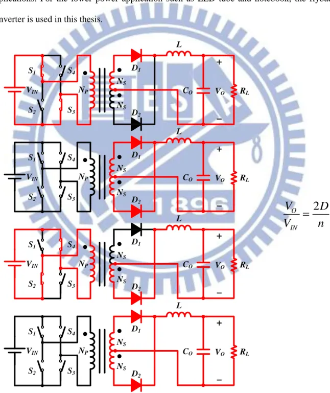
Many types of isolated converter are designed for different application according to the
output voltage and load current. And the power supply designs are often tailored to specific
applications. For the lower power application such as LED tube and notebook, the flyback
converter is used in this thesis.
CO VO RL NS NS NP VIN D1 D2 L S4 S3 S1 S2 CO VO RL NS NS NP VIN D1 D2 L S4 S3 S1 S2 CO VO RL NS NS NP VIN D1 D2 L S4 S3 S1 S2 CO VO RL NS NS NP VIN D1 D2 L S4 S3 S1 S2
2
O INV
D
V
n
1.2 Motivation
Almost all high-performance portable products use rechargeable batteries, because it is
reusable for green energy. Also the personal computer now is used to synchronous with
portable device through USB. So charging the battery from AC input through USB becomes
the important issue in nowadays. The most common charging method in present days is the
CC-CV (Constant Current-Constant Voltage) method. First, the charger charges the battery in
constant current to the specified voltage. Once the battery reaches the rated voltage, the
charger enters the constant voltage mode and keeps the battery in stable voltage.
To protect the battery from being overcharged, the charging process needs to switch
from CC phase to CV phase to gradually reduced the charge current until the process is
finished [8] [9]. So the transition time of two phases is also needed to be carefully designed.
How to sense the correct output voltage and current is the key point to changing precisely
from CC to CV.
This thesis proposed a robust isolated switch-mode charger instead of a conventional
charger to guarantee the protection for application of portable product. For the entire isolated
converter, flyback converter appears commonly in the electrical devices around modern
people because of the lower output power application. The combination of flyback converter
for charger application is called primary side regulator (PSR). This proposed PSR is using
self-calibration knee voltage detection (KVD) technique to achieve the correct sensing voltage.
By changing the CC and CV phase precisely to prevent overcharge, it can also enhance the
1.3 Thesis Organization
The thesis introduces the isolated charger PSR based on flyback converter and charging
sequence. The basic concept and operation of flyback converter organized in Chapter 2. The
proposed CC and CV regulation method compare to conventional is described in Chapter 3.
The circuits implementations are demonstrate in Chapter 4.
Finally, the whole system chip simulation, simulation specification, conclusions and
Chapter 2
Basic Definition Principles of Flyback
Converters
From the previous discussion, the isolated converter plays an important role in the use of
high input voltage application. Also the flyback converter has many advantages in low power
application. In order to understand the concept of the flyback converter, this chapter first
described the operation of flyback converter in different modes. In addition, the consideration
between modes is described in this chapter. The efficiency also considered into the operation.
One of the control methods named Quasi-Resonant (QR) is used in the CV regulation to save
the efficiency. Besides, the non-ideal effect is demonstrated after the modes description. These
non-ideal factors affect the design of this topology. Then the efficiency and losses of the
2.1 The Basic Operation of Flyback Converter
All of the DC-DC converters’ operation can be classified into discontinuous conduction
mode (DCM) and continuous conduction mode (CCM) according to its switching timing.
Continuous conduction mode means that the current in the energy transfer inductor never goes
to zero between switching cycles. In discontinuous conduction mode (DCM) the current goes
to zero during part of the switching cycle. Flyback converter can be operated in both modes
depending on whether the primary inductance of the transformer is completely demagnetized
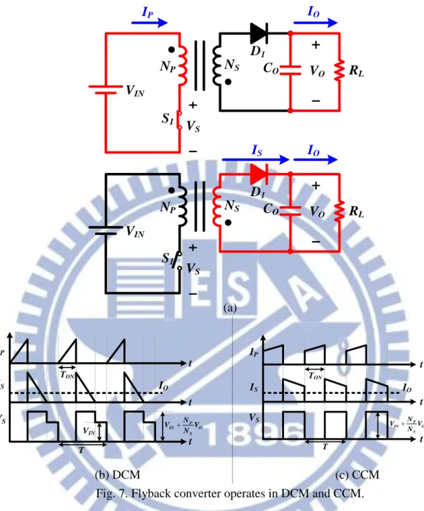
or not. Fig. 7 shows the ideal waveform of flyback converter operating in DCM and CCM.
The flow current of IP and IS represent the transformer’s primary winding current and
secondary winding current. IO is the average current of output. And the VS mean the voltage
across power switch.
In DCM operation, the primary side current rises with the slope VIN/Lm during the on
time of power switch. Lm is the magnetizing inductance of transformer. And the secondary
current falls with the slope VIN/Lm, when the switch turns off. Therefore, it makes the current
form a triangular wave. During the on time, the voltage across switch is the sum of input
voltage and reflected voltage from output. Once the secondary current decreases to zero, the
drain voltage drops to VIN. On the other hand, the CCM operation makes the transformer’s
VIN CO RL NP NS V O D1 S1 VIN CO RL NP NS VO D1 S1 IP IS IO IO VS VS (a) IS IO IP VS TON VIN t t t T P IN O S N V V N IS IO IP VS TON t t t P IN O S N V V N T (b) DCM (c) CCM
Fig. 7. Flyback converter operates in DCM and CCM.
To analyze the DCM and CCM in detail, each mode has its own advantages and
drawbacks. The DCM operation has many merits such as the zero turn on losses for the power
switch, good line and load transient response, the feedback loop has only single pole is easy to
stabilize, the smaller transformer size because of the sharper current slope, and the recovery
time of rectifier is not critical that means current is zero well before reverse voltage is applied.
But DCM operation still have some disadvantage such as the larger output ripple and high
The CCM operation is only good at small output ripple and the peak current of rectifier
and switch is half the value of discontinuous mode. And its drawbacks are the rectifier losses
of recovery time and the loop is difficult to stabilize owing to the two poles and right half
plane zero.
TABLE II shows the comparison table of the flyback converter’s operation between
DCM and CCM. The blue color means the better performance than the other, and the red is
opposite. Consequently, according to the table, the DCM operation in flyback converter has
more advantages, so the DCM operation is common in flyback converter’s control IC.
In general, flyback converter appears commonly in the electrical devices around modern
people because of the lower output power application. Flyback converter has been employed
operating both in continuous conduction mode (CCM) and discontinuous conduction mode
(DCM) as well as critical conduction mode (CRM), boundary between CCM and DCM.
Compared with CCM, BCM enjoys benefits such as soft switching, fast transient response,
smaller transformer, and easier compensation for system’s stability [10] - [12].
TABLE II
Comparison of flyback converter operating at CCM and DCM
DCM CCM
Transformer size Small Large
Peak current of switch Large Small
Output ripple Large Small
Recovery time rectifier Small Large
Loop compensation Easy Hard
Line/Load transient response Fast Slow
2.2 Non-Ideal Phenomenon of Flyback Converter in
DCM
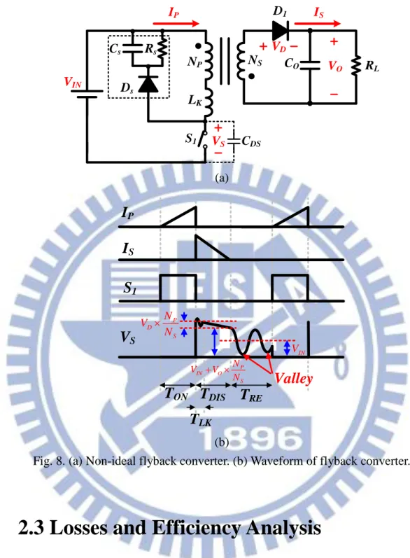
The concept of flyback converter introduced in section 2.1 is the ideal. But flyback
converter has non-ideal phenomenon. This section is describing the non-ideal when realize the
flyback converter. First of all, the transformer has magnetizing inductance Lm. However,
transformer also has leakage inductance LK as shown in Fig. 8 (a). Leakage inductance is the
property of an electrical transformer that causes a winding to appear to have some inductance
in series with the mutually-coupled transformer windings. This is due to imperfect coupling of
the windings and creation of leakage flux which does not link with all the turns of the winding.
The leakage flux alternately stores and discharges magnetic energy with each electrical cycle
and thus effectively acts as an inductor in series in each of the primary and secondary circuits.
Leakage inductance is primarily caused by the design of the core and the windings.
To reduce the effect of LK to the system, a simple circuit called snubber is applied, which
composed by CS, RS and DS in Fig. 8 (a). It can be used in electrical systems with an inductive
load to suppress instantaneous voltage spike across the power switches in case of sudden
current flow. Transient voltage variation will be a source of electromagnetic interference (EMI)
in other circuits. Additionally, if the instantaneous voltage spike across the device is beyond
what the devices can tolerate, it may damage or destroy the devices. Thus, the snubber
provides a short-term alternative current path around the current switching device so that the
inductive element may be discharged more safely and quietly.
Inductive elements are often unintentional, but arise from the current loops implied by
physical circuitry. While current switching is everywhere, snubbers will generally only be
required where a major current path is switched, such as in power supplies. Snubbers are also
interference and welding/sticking of the contacts that can occur. In flyback converter, snubber
is used to give a path to leakage inductance’s resonant.
Second, the switch S1 has the parasitic capacitor CDS. It is an unavoidable and usually
unwanted capacitance that exists between the parts of an electronic component. All actual
circuit elements such as inductors, diodes, and transistors have internal capacitance, which
can cause their behavior to depart from that of 'ideal' circuit elements. In addition, there is
always non-zero capacitance between any two conductors. Also the forward diode D1 has the
forward drop VD.
When switch turn off, the primary side current IP is down to zero as shown in Fig. 8 (b).
The magnetizing inductance Lm start to transfer energy to secondary side and make the current
IS starts to discharge. But there is only the magnetizing inductance can transfer energy, the
leakage inductance has no path to secondary can discharge energy. Leakage inductance can
only discharge to parasitic capacitor CDS, and VS start the first resonant in TLK cause by LK and
CDS. Also VS reflect the output voltage VO and forward voltage VD. The forward voltage VD is
decreasing with IS decreasing. When secondary current is discharging to zero, the forward
voltage VD is also zero. The reflected voltage only remain VO. VS is VIN+(NP/NS)VO at the end
of discharge time. Also the charges in CDS start to discharge to Lm and resonant to each other
until next cycle. The resonant of CDS and Lm makes the VS have many valleys in TRE. It can
make the valley voltage down to nearly zero. By using these valleys properly, the flyback
converter can turn to the next cycle in soft switching and improve the efficiency. This soft
switching technique by turning on the switch when resonant to valley is also called
VIN CO RL NP NS VO D1 S1 LK CDS VS VD IP IS Rs Ds Cs (a)
S
1V
SI
PI
S P IN O S N V V N P D S N V N T
ONT
DIST
RE IN VT
LKValley
(b)Fig. 8. (a) Non-ideal flyback converter. (b) Waveform of flyback converter.
2.3 Losses and Efficiency Analysis
Power loss of switching regulators is the combination of the switching loss and the
MOSFET’s conduction loss as shown in equation (1). The power loss is important factor to
determine efficiency and it is briefly introduced as following.
MOSFET SW COND
2.3.1 Conduction Loss
The conduction loss is mainly related to high-side transistor loss and low-side transistor
loss. High-side conduction loss is calculated straightforward that is just the I R2 loss timing
the MOSFET’s duty cycle as below:
Where RDS ON( ) is at the maximum equivalent resistor on operation MOSFET.
In the same way, low-side conduction loss is determined as (3).
2.3.2 Switching Loss
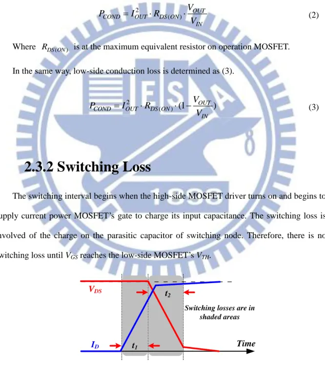
The switching interval begins when the high-side MOSFET driver turns on and begins to
supply current power MOSFET’s gate to charge its input capacitance. The switching loss is
involved of the charge on the parasitic capacitor of switching node. Therefore, there is no
switching loss until VGS reaches the low-side MOSFET’s VTH.
2 ( ) OUT COND OUT DS ON IN V P I R V (2) 2 ( ) (1 ) OUT COND OUT DS ON IN V P I R V (3) Time
Switching losses are in shaded areas
VDS t
2
t1
ID
When VGS reaches VTH, the input capacitance of gate is being charged and the MOSFET’s
drain current ID is rising up linearly until it reaches the current IL which is presumed to be
ILOAD. During this period (t1) the MOSFET is sustaining the entire input voltage VIN across it,
the energy in MOSFET during t1 is:
1 1
(
2
)
IN LOAD t
V
I
P
t
(4)Sequentially, as the beginning time of second period t2, the current flowing through
high-side MOSFET is ILOAD, and the VDS begins to fall. All of the gate current will be going to
recharge CGD. CGD is similar to the “Miller” capacitance of transistor, so t2 could be thought of
as “Miller time”. During this time the current is constant as ILOAD and the voltage is falling
fairly linearly from VIN to 0, therefore:
2 2
(
2
)
IN OUT t
V
I
P
t
(5)The total switching loss for any given edge is just the power that occurs in each
switching interval, multiplied by the duty cycle of the switching interval:
1 2
(
) (
)
2
IN OUT SW SV
I
P
t
t
F
(6)2.3.3 Quiescent Loss
The quiescent loss also called as static loss that was consumed by other controllers of
switching regulators. The smaller quiescent loss also causes higher efficiency.
Q IN Q
P
V
I
(7)2.3.4 Efficiency
The efficiency of switching regulator is defined as the ratio of the output power
consumption and input power supplies, which is formed as below equation (8):
100%
OUT OUT ff IN O SW COND Q ElseP
P
E
P
P
P
P
P
P
(8)The total power consumption of input power supplies is involved of the output
consumption (PO), switching loss (PSW), conduction loss (PCOND), quiescent loss (PQ), and
other losses (PElse) in parasitic elements. A high efficiency results in a high performance
Chapter 3
The Proposed Primary-Side Regulator with
Self-Calibration Knee Voltage Detection
(KVD) Technique
In this chapter, the primary-side regulator (PSR) is adopted to the design of flyback
converter to show some significant advantages compared to conventional flyback converter.
Furthermore, the self-calibration knee voltage detection (KVD) technique is presented to get
rid of the disadvantage of inaccuracy caused by the remove of the feedback path from the
opto-coupler. That is to say, the charger implemented by the PSR flyback converter must have
the precise sensing technique, self-calibration knee voltage detection (KVD) technique, to
ensure accurate charging process.
3.1 Significant Advantages of PSR Flyback
Converter Compared to Conventional Design
Figs. 10 (a) and (b) illustrate the architecture of conventional flyback converter and the
PSR flyback converter, respectively. In Fig. 10(a), conventional flyback converter uses one
feedback from the secondary side through the use of the opto-coupler. Unlike the power stage
discussed in chapter 2, the transformer also includes the auxiliary winding NA to reflect the
the start-up procedure is ended. The opto-coupler and the TL431 work as the error amplifier
to get the output voltage information, VFB.
The PSR as shown in Fig. 10 (b) is similar to flyback converter mostly. The difference
between flyback converter and PSR is the external components of opto-coupler and TL431.
Instead sensing output voltage by external component, PSR is using auxiliary winding NA to
replace it. Compared with the conventional secondary-side regulation approach, the PSR can
reduce the total cost, component count, size and weight.
VGD VCS VAC 90V~264V VIN CIN RCS VO RA1 RA2 Rs Cs DA Ds NP NS NA CDD DO VA IO CO Flyback controller VSS VDET VDDH VHV IS − + VD IP VDrain Rfb1 Rfb2 CC RC Opto-coupler TL431 CF VFB RL Feedback netwrok (a) VGD VCS VAC 90V~264V VIN CIN RCS VO RA1 RA2 Rs Cs DA D s Power NMOS NP NS NA CDD DO VA IO CO
PSR controller
VDET VDDH VHV IS − + VD IP VDrain VSS (b)3.2 The Conventional Control of PSR
Conventional PSR system structure is depicted in Fig. 10 (b). The input bulk capacitor
CIN is used after full-bridge rectifier to reduce the AC line voltage ripple, which has the
switching frequency of 120 Hz. Thus, the VIN has a near DC voltage. Besides, the current
sensing resistor RCS is used to sense input line current. The auxiliary winding NA can notonly
sense the output voltage VO through the voltage divider (RA1 and RA2) to get the voltage VDET
for the controller but also provide the power to the VDDH if the controller works correctly.
Fig. 11(a) shows the basic operation of PSR. Instead of using secondary feedback
components, the PSR can use the auxiliary winding to get the information of the output
voltage VO. During the inductor current discharge time TDIS, the summation of the output
voltage VO and the diode forward voltage drop VD is reflected to the auxiliary winding as the
signal VA. It is hard to get only the VO information without being affected by the VD from the
VA. Fortunately, at the end of the diode conduction time as depicted in Fig. 11(b), the auxiliary
winding voltage simply reflects the VO because the diode forward voltage drop decreases to
zero as the diode forward current decreases to zero. By sampling the winding voltage at the
end of the diode conduction time, the VO information can be obtained as the knee voltage,
(NA/NS)*VO.
V
ODuring T
ONI
PV
INV
GDV
INV
ODuring T
DISI
SV
GD (a)V
GDV
AI
PI
S A O S N V N A D S N V N T
ONT
DIS PK I P PK S N I N T
REknee voltage=
INV
(b)Fig. 11. (a) Operation of the PSR power stage. (b) Knee voltage reveals the VO information.
Several literatures have been proposed to accurately get the information of knee voltage
[13] - [15]. Sampling pulse generator as depicted in Fig. 12 (a) is used to emulate the charging
and discharging of the inductor current [13]. The current source I1 combine with n-transistor
M1 and capacitor C1 are used to be a delay circuit. The I4, M4 and C3 also do the same work.
When the gate signal VGD is on, the p-transistor M2 is also turned-on. The current source I2
then charges the capacitor C2 to produce a charge time. When VGD is off, the n-transistor M3 is
turned-on. The capacitor C2 is discharged by current source I3 to produce discharge time that
is proportional to the charge time. When the voltage across C2 is discharged to zero, it also
means the discharge time is over. Then sampling pulse VSP is triggered to sample VA asknee
voltage.
However, the discharging slope of inductor current is proportional to the output voltage
VO. When output voltage is not equal to expected voltage, some error operation will occurred
as depicted in Fig. 12 (b). If the expected voltage higher then output voltage, the too early
operation will occur and the sampling voltage will higher than knee voltage. On the other
hand, if the expected voltage lower then output voltage, the too late operation will occur and
the sampling voltage will lower than knee voltage. In worst case, it may sample the zero
On the other hand, the regulation of VO can be changed to regulate the summation of the
VO and the VD. In [14], the summation of the VO and the VD can be derived by the proposed
circuit in Fig. 13 (a). The VO is expected to be regulated to VREF. The VD information can be
got by the primary side current signal VI. Therefore, the new reference VREF1 is equal to
3 1 2 I REF ext V R V R R R
. That is to say, if the sampling voltage in the beginning of the
discharging period after a blanking time should be regulated to VREF1, the VO can be
approximately regulated to the VREF as shown in Fig. 13 (b).
VGD VSP M1 M2 M3 M4 C1 C2 C3 I1 I2 I3 I4 (a) VGD VA I1 I2
Correct operation Too early operation Too late operation VSP
(b)
Fig. 12. (a) Sampling pulse generator. (b) Sampling pulse with different expected
However, the disadvantage is that it needs the external resistor Rext. Because of the
different forward diode has different forward voltage VD. Using the same resistor cannot
emulate different VD correctly. An external resistor increase the cost and component count.
In [15], one RC circuit is utilized to generate a delayed waveform VDELAY of the signal
VDET from the auxiliary winding. The original signal VDET is used to determine the sampling
time of the knee voltage from the VDELAY. That is to say, in the beginning of the resonant
period TRE when the inductor current decreases to zero, the slope of the VDET becomes
extremely sharp. By comparing the slope of VDET to a threshold value, it can determine if the M1 M2 M3 R1 M4 M5 M6 R2 VI VREF R3 Rext 1 I V R 1 2 ext I R V R R 1 3 1 2 I
REF REF Rext R V V V R R (a)
V
GDV
AI
1I
2T
ONT
DIST
RE B la n k in gV
SPRegulate to V
REFRegulate to V
REF1 (b)VDET is in resonant period or not. Then sample the VDELAY for knee voltage as depicted in Fig.
14.
However the slope of VDET in resonant period depends on the LC values, which are
transformer’s magnetizing inductance Lm and power MOSFET parasitic capacitor CDS. By
using constant value compare to the slope of VDET to determine the sampling time also needs
to adjust the RC values for VDELAY according to different LC values that can sample the correct
knee voltage. In order to adjust the RC value, it needs external components. That also increase
the cost and component count.
3.3 The Proposed Charger by the PSR Controller
with the KVD Technique
The proposed PSR controller with the KVD technique is shown in Fig. 15. Similarly, the
DCM is utilized in the PSR controller. Here, the PSR controller is used to control the charging
process of the Li-Ion battery. That is to say, the PSR controller needs to have two control
loops to provide the charging procedure of the constant current (CC) and the constant voltage
(CV) stages.
V
DETV
DELAY2. S/H the knee voltage by VDELAY
1. When VDET slope is sharp enough
The current information VCS in (9) is derived from the primary side current IP flowing
through the sensing resistor RCS, which is connected between the source of the power
MOSFET and ground.
,
and where is the peak current.
CS P CS CS PK PK CS PK
V I R V I R I (9)
The VI is proportional to the integration of the peak current information IPK within
one discharging time TDIS in the current calculator circuit. Here, the TDIS can be used to
decide the integrating time. In the current loop, the modulation of the on-time of the CC stage
is decided by the comparison result of the VRAMP and the VERR_I, an error signal derived at the
output of the error amplifier 1 (EA 1). As a result, the VI can be regulated to the reference
voltage VREF_I to ensure constant current. Here, the CC stage is controlled by a constant
switching frequency, which is determined by the oscillator OSC with a pulse signal VPULSE as
depicted in Fig. 16.
Here, the secondary side peak current IS,PK can be expressed by the IPK and shown in (10)
according the turn ratio of NP/NS where the primary winding and the secondary winding have
NP turns and NS turns, respectively.
, , CS PK P P S PK PK S CS S V N N I I N R N (10)
Thus, the average output current can be expressed as (11).
, , 1 2 O avg S PK DIS S I I T T (11)
Substituting for IS,PK from (10) gives (12).
, , 1 2 P O avg S CS PK DIS CS S N I T R V N T (12)
Interestingly, in the design of the PSR control, only two variables VCS,PK and TDIS are
needed to be determined. That can easily achieve CC regulation with constant switching
On the other hand, the other voltage loop is used for constant voltage (CV) stage. From
the auxiliary winding NA in Fig. 10(b), the voltage information VDET is a scaled down value of
the VA by the voltage divider, composed of the resistors RA1 and RA2. The knee voltage
detector (KVD) and the self-calibrator circuit are designed to get accurate output voltage
information. Thus, the knee voltage VV can be got without being affected by the diode forward
voltage VD. The VV can be regulated to be close to the reference VREF_V by the voltage loop. In
VCS Current Calculator Knee Voltage Detector Self-Calibrator VREF_I VDET TDIS VCA VPK1 VPK VREF_V COMP 1 OSC S Q R VGD VERR_V VERR_I VRAMP VPLUSE VI VV VPWM VCV EA 1 EA 2 COMP 2
Fig. 15. Proposed PSR controller.
PK I VGD VA IP IS TDIS TS P PK S N I N , O avg I VPULSE VRAMP VERR_I P PK S N I N PK I TDIS TS
the CV stage, the error signal VERR_V and the current sense signal VCS are used to determine the
on-time value as shown in Fig. 17. Besides, the switching frequency varies with the value of
VERR_V. If the VERR_V becomes smaller, the switching frequency will be extended by the
OSC circuit to reduce the switching power loss because the Quasi-Resonant (QR) technique
is also used for zero voltage switching (ZVS) to improve the efficiency if there is a small
input current.
Fig. 18 shows the charging procedure of the battery charger. It includes the CC and the
CV stages. In the CC stage, the output voltage VO is charged from the minimum voltage VO,min
to the nominal full-charged voltage VO,max with a constant switching frequency, which is equal
to 1/TS. The value of the VO,max doesn’t exceed the tolerance of the maximum allowable
voltage of the battery while the VO,min can ensure the PSR operates in the DCM.
The discharging current rate is proportional to the VO as shown in (13). ,where Lm is the
magnetizing inductance of the transformer.
S P O S m dI N V dt N L (13)
In Fig. 17, the IPK and the TDIS can be derived as shown in (14) and (15), respectively. VGD VERR_V VCS VA Ip Is VPULSE VV VV TDIS TS TDIS TS TON TON
where IN PK ON ON S m V I T T DT L (14) , 2 S PK PK P IN DIS ON S O P O P O S m S m I I N V T T N V N V N V N L N L (15)
In case of minimum output voltage VO,min, the TDIS in (15) has a maximum value of
TDIS,max. To ensure the discharging phase can be finished within one constant switching period
TS, the inequality in (16) should be made. That is, the operation is always kept in the DCM
due to the inductor current can be decreased to zero within one switching period.
,max ,min S IN DIS ON P O S O ON N N V T T N T T T V (16)
Therefore, the initial point of the output VO,min for the CC operation can be derived as
shown in (17). ,min 1 S O IN P D N V V D N (17)
In other words, the startup circuit should ensure the output voltage is charged to VO,min
first. Then, the charger is switched to the CC operation with a constant current defined by the
reference voltage VREF_I. Once the output is charged to the VO,max with a constant switching
freuqency, the charger will be changed to the CV operation. In CV operation, the switching
frequency varies with the value of the VERR_V. Besides, the QR technique is effectively used to
decrease the switching frequency for high efficiency. Consequently, the VO is finally regulated
The transition from the CC to the CV is depicted in Fig.19. The on-time value is
determined by the VRAMP and the VERR_I in the CC operation. On the other hand, the on-time
value is determined by the VERR_V and the VCS. In the beginning of the charging procedure, the
duty cycle is determined by the CC operation because the duty cycle decided by the CV
operation is too large under a high VERR_V. Once the VO is gradually charged to the nominal
value, the VERR_V will be pulled lower than the VERR_I. The transition from the CC operation to
the CV operation happens. In other words, the duty cycle decided by the CV operation will be
smaller than that of the CC operation. Thus, a smooth transition can be made. Here, a flag
signal VCV is used to indicate the CV operation is enabled and to decrease the switching
frequency. The CV operation uses the adaptive valley selection method to decrease the
switching frequency. The adaptive valley selection method depends on the decreasing output
current to accordingly decrease the switching frequency for reducing switching power loss in
the CV operation. Once the charging current is lower than a predefined value, the green mode
is utilized to further reduce the switching power loss. Here, the green mode uses an ultra-low
switching frequency for high efficiency.