國立交通大學
材料科學與工程研究所
博士論文
用於太陽電池之氮化矽次波長抗反射結構
用於太陽電池之氮化矽次波長抗反射結構
用於太陽電池之氮化矽次波長抗反射結構
用於太陽電池之氮化矽次波長抗反射結構
設計與樣品試製
設計與樣品試製
設計與樣品試製
設計與樣品試製
Design and Fabrication of Sub-wavelength Structures on Silicon
Nitride for Solar Cells
研 究 生:哥帝克
指導教授:張 翼 博士
Design And Fabrication of Sub-wavelength Structures on
Silicon Nitride for solar cells
研 究 生:哥帝克 Student: Kartika Chandra Sahoo
指導教授:張 翼 博士 Advisor: Dr. Edward Yi Chang
國立交通大學
材料科學與工程研究所
博士論文
A Dissertation
Submitted to Department of Materials Science and Engineering College of Engineering
National Chiao Tung University In Partial Fulfill of the Requirements
For the Degree of Doctor of Philosophy
2009
Hsinchu, Taiwan, Republic of China
Dedicated to
ACKNOWLEDGEMENT
This Ph.D. thesis was established in the Compound Semiconductor Devices
Laboratory (Department of Materials Science & Engineering) at the National
Chiao-Tung University (NCTU), and would not have been what it is today without the
support and advice of others.
I first express my greatest gratitude and thankfulness to my advisor Prof.
Edward Yi Chang, who supervised me during my entire Ph.D. study. Without his
encouragement and inspiration, this work will never been done this far. His keen
insights and intellectual comments have guided me throughout the ups and downs in
my research. What I learned from him will benefit me for a life time as both an
independent researcher and an active collaborator.
I would also like to thank Prof. Yiming Li of Department of Electrical
Engineering, National Chiao-Tung University for his help in scientific and
non-scientific advices. His valuable comments and training during the preparation of
dissertation is appreciated.
I wish to thank former and current members in Compound Semiconductor
Devices Laboratory of National Chiao-Tung University, Men-Ku Lin, S. P. Wang, C.
Dr. H. M. Lee. Discussions with them opened my viewpoints and inspired ideas.
Many thanks to all the Ph.D. students and post-docs, past and present of the
Compound Semiconductor Devices Laboratory, my office mate for more than five
years, for the very nice working atmosphere and for the very good scientific
discussions and contributions.
Furthermore, I want to thank National Science Council (NSC), Taiwan and
Motech Industries Inc. (MOTECH), Taiwan for sponsoring our projects.
A special thank to my parents for their moral support and faith on me during
all these years.
At last I wish to thank my lovely wife without whose support I couldn’t have
completed this thesis. Her constant encouragement and support during my ups and
downs helps me to finish my work with productivity.
用於太陽電池之氮化矽次波長抗反射結構
用於太陽電池之氮化矽次波長抗反射結構
用於太陽電池之氮化矽次波長抗反射結構
用於太陽電池之氮化矽次波長抗反射結構
設計與樣品試製
設計與樣品試製
設計與樣品試製
設計與樣品試製
研究生:哥帝克 指導教授:張 翼 博士 國立交通大學材料科學與工程研究所 摘要 摘要 摘要 摘要 本論文首先以數值模擬計算太陽電池之氮化矽次波長抗反射結構。根據理論 的分析,吾人進而發展樣品試製方法去製作氮化矽次波長結構。氮化矽是一種常 用於半導體上的反射結構層材料,吾人藉此次波長結構當成第二抗反射層,使得 完整樣品的結構為雙層抗反射層。此種雙層抗反射結構成本低並具有不錯的太陽 電池的光、電特性。 模擬上我們是使用嚴謹的波偶合法進行反射率計算,研究上吾人是對一理想 化的金字塔型的氮化矽次波長抗反射結構進行反射率對照射波的計算。其中單層 抗反射層、雙層抗反射層皆一一加以分析比較,進而找出較佳的幾何結構比,及 其伴隨的有效反射率。藉由理論分析的結果,吾人運用自組裝鎳奈米粒子以及誘 導式電漿離子偶合蝕刻提出一個簡單且可控制比例的製程步驟。藉此法在矽基板 上以鎳薄膜厚度去控制鎳奈米粒子的大小與密度。由於次波長結構的表面形成與 反應式離子蝕刻的條件密切相關,因此研究上也探討誘導式電漿離子偶合蝕刻製 程條件對於氮化矽次波長抗反射結構成長的影響。吾人藉由實驗已找出蝕刻時間 與結構幾何比例以及反射率的關係。總之,本研究已經完成適用於太陽電池之氮化矽次波長抗反射結構的理論與 實驗研究。未來可以研究不同次波長結構形狀的製程以及反射率之相關議題。
Design and Fabrication of Sub-wavelength Structures
on Silicon Nitride for solar cells
Student: Kartika Chandra Sahoo
Advisor: Dr. Edward Yi Chang
Department of Materials Science and Engineering
National Chiao Tung University
Abstract
In this dissertation, we numerically study the reflectance of sub-wavelength structures on silicon nitride for solar cell application. Based on the numerical study, we develop a fabrication method to form the sub-wavelength structures on silicon nitride surface for solar cells. Since silicon nitride is a well known antireflection coating used in semiconductor industry, we explore the texturization on silicon nitride antireflection coating and its optical properties. The main motivation behind this lies in the fact that the sub-wavelength structures will act as a second antireflection coating layer with an effective refractive index so that the total structure can perform as a double layer antireflection coating layer. Thus, we could cost down the deposition of second antireflection coating layer can be saved with better or comparable performance as that of a double layer antireflection coating solar cell.
In this study, we calculate the spectral reflectivity of pyramid-shaped silicon nitride sub-wavelength structures. A multilayer rigorous coupled-wave approach is advanced to investigate the reflection properties of silicon nitride sub-wavelength structure. We examine the simulation results for single layer antireflection and double layer antireflection coatings with sub-wavelength structure on silicon nitride surface, taking into account effective reflectivity over a range of wavelengths and solar efficiency. The results of our study show that a lowest effective reflectivity of 3.43% can be obtained for the examined silicon nitride sub-wavelength structure with the height of etched part of silicon nitride and the thickness of non-etched layer of 150 nm and 70 nm, respectively, which is less than the results of an optimized 80 nm silicon nitride single layer antireflection coating (~ 5.41%) and of an optimized double layer antireflection coating with 80 nm silicon nitride and 100 nm magnesium fluoride (~5.39%). 1% cell efficiency increase is observed for the optimized Si solar
cell with silicon nitride sub-wavelength structure, compared with the cell with single layer silicon nitride antireflection coatings; furthermore, compared with double layer antireflection coated solar cell, the increase is about 0.71%. The improvement on the cell efficiency is mainly due to lower reflectance of silicon nitride sub-wavelength structure over a wavelength region from 400 nm to 600 nm that leads to lower short circuit current.
Based upon our theoretical calculation of improved efficiency of silicon solar cell with silicon nitride sub-wavelength structures, we have developed a simple and scalable approach for fabricating sub-wavelength structures on silicon nitride by means of self-assembled nickel nano particle masks and inductively coupled plasma ion etching. The size and density of nickel nano particles are controlled by the initial thickness of nickel film that will be annealed to form the nano-particles on the silicon nitride film deposited on the silicon substrate. Inductively coupled plasma etching time is responsible for controlling the height of the fabricated silicon nitride sub-wavelength structure on silicon substrate.
Nevertheless, the surface profile of a sub-wavelength structure is strongly dependent on the conditions of the reactive ion etching process. So, we have also investigated the effect of inductively coupled plasma etching conditions on the profile of fabricated sub-wavelength structure on Silicon nitride antireflection coating layers. At last, we succeeded in fabrication of nanopillar structures and nanocone structures on silicon nitride surface by one step and two step inductively coupled plasma etching methods. The relationship of etching time with structure height and average reflectance spectra has been drawn.
In summary, design and fabrication of sub-wavelength structures on silicon nitride antireflective surface was investigated for the first time. The structure height and non-etched part of silicon nitride has been optimized for lowest effective reflectance by theoretical calculation using rigorous coupled wave analysis method. Also the shape effect has been studied theoretically. Based on theoretical results, the nanopillar and nanocone structures on silicon nitride surface have been fabricated successfully using self-assembled nickel nano clusters and inductively coupled plasma etching method. The achieved low reflectance is believed to be useful to improve the efficiency of solar cells. Also, the preliminary results for a silicon solar cell has been obtained using silicon nitride sub-wavelength structure, which shows a great promise in improvement of efficiency compared with a single layer antireflection coating.
Contents
ACKNOWLEDGEMENT ...IV
Abstract in Chinese...VI
Abstract in English...VIII
Contents ...X
Tables...XII
Figures ...XIII
Chapter 1 Introduction ... 1
1.1 Introduction to solar cell ...1
1.2 Solar Cell figures of merit ...4
1.2.1 Voltage and current...4
1.2.2 Efficiency ...5
1.2.3 Natural Limits of Efficiency...6
1.3 Antireflection Coatings...9
1.3.1 Single Layer Antireflection Coatings ...9
1.3.2 Multi-layer Antireflection Coatings... 11
1.4 Sub-wavelength Structures...12
1.5 Motivation ...13
1.6 Thesis content ...15
Chapter 2
Design and Simulation of Silicon Nitride SWS... 17
2. 1 Sub-wavelength structure design ...17
2.1.1 Theory and Simulation Procedure...17
2.1.2 Results and Discussions...22
2.2 Shape Effect...31
2.2.1 Simulation Procedure...31
2.2.2 Results and Discussion...33
2.3 The Electrical Characteristics Calculation ...39
2.3.1 Introduction to PC1D software ...39
2.3.2 Simulation Procedure...41
2.3.3 Simulation Settings ...42
2.3.4 Results and Discussion...43
Chapter 3
Fabrication Processes and Measurements ... 47
3.1 Sub-wavelength structure Fabrication Process ...47
3.1.1 Wafer Clean ...48
3.1.2 Deposition of Silicon Nitride ...48
3.1.3 Nano-mask Formation ...50
• Deposition of Metal ...51
• Rapid Thermal Anneal...51
3.1.4 Inductively Coupled Plasma (ICP) Etching ...52
3.1.5 Nano-mask Removal ...52
3.2 Characterization Methods...53
3.2.1 Morphology Analysis ...53
3.2.2 Reflectance Measurement ...53
3.3 Results and Discussion ...53
3.3.1 Process optimization of Nanomask for silicon nitride SWS...53
3.3.1.1 RTA temperature optimization ...53
3.4.1.2 Initial Nickel Thickness optimization ...55
3.3.2 Height optimization of silicon nitride SWS...58
3.4 Results Comparison ...64
3.4.1 Comparison of measurement and simulation...64
3.4.2 SWS Comparison with SLAR & DLAR...66
3.5 Summary ...68
Chapter 4
Fabrication of Nanocones ... 69
4.1 Experimental ...69
4.2 Results and Discussions ...70
4.4 Summary ...79
Chapter 5
Solar Cell Fabrication ... 80
5.1 Fabrication Process...80
5.2 Results and Discussion ...82
5.3 Summary ...84
Chapter 6
Conclusions and Future Works... 85
6.1 Conclusion...85
6.2 Future Work...87
Appendices... 89
References... 96
Tables
Table 1. Effective reflectivity for those optimized structures of 150 nm Si3N4 SWS and 70 nm non-textured Si3N4 film, compared with the Si SWS, Si3N4 SLAR (its thickness is 80 nm) and Si3N4 / magnesium fluoride DLAR (its thickness is 80 nm / 100 nm) structures. ... 31
Table 2 Deposition Condition for Silicon Nitride by PECVD... 50
Table 3: The height of the fabricated Si3N4 SWS with different etching time, for Sample-3. ... 62
Table 4: Average residual reflectivity calculated by the equation (37) for measured reflectance of bare silicon, 69.1 nm silicon nitride deposited on silicon, 69.1 nm silicon nitride & 56 nm MgF2 double layer deposited on silicon and 140 ~ 160 nm silicon nitride SWS fabricated on silicon. ... 67
Table 5: Measured Solar Cell parameters for Silicon Nitride SLAR and Silicon Nitride SWS. The difference is also tabulated. ... 83
Figures
Figure 1.1 A schematic of simple conventional solar cell [50]... 2
Figure 1.2 Solar Radiation Spectrum. ... 3
Figure 1.3: J~V characteristics and Maximum power ... 5
Figure 1.4: Theoretical maximum levels of efficiency of various solar cells at standard conditions [51]. ... 7
Fig. 1.6: Schematic of different material structure (a) two layers without ARC (b) Three layers with ARC... 9
Figure 1.7 Diagram of antireflection coatings with (a) SiO2/TiO2 double layers and (b) SiO2/SiO2–TiO2/TiO2 triple layers. ... 12
Figure 1.8 Schematic of a Sub-wavelength grating structure... 13
Figure 2.1: (a) Geometry of sub-wavelength structure studied in this work, where h is the height and s is the non-etched part of SWS. (b) A stack of uniform homogeneous layers resulting from the partitioned geometry of (a) for the reflection calculation using the multilayer RCWA method and EMT. ... 18
Figure 2.2: (a) The schematic of Si and Si3N4 SWS for the study. (b) The reflectance versus the wavelength for Si SWS with h = 88 nm and Si3N4 SWS with h = 88 nm and vanished non-etched part of SWS (i.e., s = 0 nm). Comparison for the Si3N4 SWS with the case of non-zero s, say s = 20 nm is also provided. It is found that it is possible to reduce the reflectance of Si3N4 SWS by proper selection of h and s... 23
Figure 2.3: The spectral reflectivity of Si3N4 SWS for h = 68 nm and s = 20 nm with constant Si refractive index and refractive index as a function of lambda given by Eq. (28). ... 25
Figure 2.4: Refractive index of Si vs wavelength using equation (28) ... 25
nm; plot is as a function of (a) h for Si SWS and (b) of h and s for Si3N4
SWS. ... 27
Figure 2.6: Plot of the effective reflectance for the wavelength varying from 400 nm to 1000 nm. (a) is the result as a function of the thickness of Si3N4 ARC with n = 2.05 for SLAR coating on Si. (b) is the result as a function of the thickness of ARC 2 and refractive index of ARC 2 for Si3N4 / ARC 2 DLAR coating on Si. The thickness of Si3N4 ARC 1 is fixed at 80 nm which is optimized from (a). ... 28
Figure 2.7: Comparison of the reflectance spectra among the bulk Si (i.e., the bare Si), the optimized SLAR, DLAR, Si SWS and Si3N4 SWS for the wavelength from 400 nm to 1000 nm... 30
Figure 2.8: Three model shape types (a) cone (b) parabola and (c) cylinder shape. .. 32
Figure 2.9: Comparison of the change of calculated effective refractive index at λ = 600 nm from the top of the SWS to the bottom of Si3N4 SWS ... 34
Figure 2.10: Parabola Shape optimization... 35
Figure 2.11: Cone Shape Optimization ... 35
Figure 2.12: Cylinder shape optimization ... 36
Figure 2.13: Comparison of optimized structures with different shape ... 36
Figure 2.14: The effective reflectance of Si3N4 SWS versus the SWS volume... 37
Figure 2.15: Effective reflectance Vs Base diameter w / volume (a) 100000 nm3 (b) 300000 nm3 and (c) 500000 nm3. ... 39
Figure 2.16 Device Schematic used in PC1D for solar characteristics calculation. ... 42
Figure 2.17: (a) Electrical characteristics and (b) the external quantum efficiency obtained from PC1D simulation for a silicon solar cell using the reflectance spectra for the three optimized structures, they are Si3N4 SWS, SLAR and DLAR... 44
Figure 3.1 SWS fabrication process... 47
Figure 3.2 CSD Lab PECVD machine ... 50
Figure 3.3 Rapid Thermal Anneal Process graph... 52
Figure 3.4: SEM Images of nickel nano-clusters formed after RTA for 60 sec at (a) 800 οC (b) 850 οC (c) 900 οC... 54
Figure 3.5: SEM Images of nickel nano-clusters formed after RTA at 850 0C for 60 sec (a) Sample 1 w/ initial nickel thickness 20 nm; (b) Sample 2 w/ initial nickel thickness 15 nm; and (c) Sample 3 w/ initial nickel thickness 8 nm; (d) Sample 4 w/ initial nickel thickness 3 nm. ... 56
Figure 3.6: Effect of initial nickel thickness on density and average diameter of the Ni nano-clusters after RTA at 850 οC for 60 sec. ... 57
Figure 3.7: SEM Images of fabricated Si3N4 SWS w/ ICP etching time (a) 60 sec; (b) 100 sec; (c) 120 sec for Sample-4... 59
Figure 3.8: Effect of etching time on the average height of fabricated Si3N4 SWS. .. 60
Figure 3.9: Comparison of reflectance spectra for the fabricated Si3N4 SWS with different etching time, for Sample-4. ... 60
Figure 3.10: SEM Images of fabricated Si3N4 SWS w/ ICP etching time (a) 90 sec; (b) 120 sec; (c) 180 sec for Sample-3... 62
Figure 3.11: Comparison of reflectance spectra for the fabricated Si3N4 SWS with different etching time, for Sample-3. ... 63
Figure 3.12: SEM Image of fabricated Si3N4 SWS w/ ICP etching time 120 sec ... 63
Figure 3.13: Comparison of reflectance spectra of sample-3 and sample-4 for ICP etching time 120 sec, where the average heights of Si3N4 SWS were 155 nm and 175 nm, respectively. ... 64
Figure 3.14: Comparison of fabricated Si3N4 SWS with Simulated Si3N4 SWS w/ h = 155 nm and s = 65 nm, for the wavelength range from 400 nm to 1000 nm.
... 65
Figure 3.15: Comparison of the reflectance spectra among the bulk Si (i.e., the bare Si), the optimized SLAR, DLAR, and Si3N4 SWS for the wavelength from 400 nm to 1000 nm. ... 66
Figure 4.1: Schematic of fabrication process of (a) silicon nitride nanopillars (b) silicon nitride nanocones. ... 70
Figure 4.2: SEM images of Ar plasma etching of nickel nano cluster on silicon nitride for (a) 30 s (b) 120 s. SEM images of CF4/O2 plasma etching of nickel nano cluster on silicon nitride for (a) 60 s (b) 120 s. ... 72
Figure 4.4 : SEM images (top-view) of fabricated nanocone structures on silicon nitride film using two-step etching process for etching time: (a) 90 s (b) 120 s (c) 150 s. Cross-section SEM view of the fabricated nanocone structures with etching time (d) 90 s and (e) 180 s. ... 74
Figure 4.5: Schematic illustration of the base of the fabricated nanocones: (a) shortest etching time (b) medium etching time, and (c) longer etching time... 75
Figure 4.6 : Relations of etching time with (a) Average reflectance and (b) Structure height for the fabricated nanocone and nanopillar structures on silicon nitride film. (c) The reflectance spectra comparison of nanocone and nanopillar structures with almost same height for the wavelength from 190 to 1000 nm. ... 77
Figure 5.1: Fabrication process steps for Solar Cell with SWS (a) Emitter process ( done at MOTECH Lab) (b) SWS Process (done at CSDLAB) (c) Post process (done at MOTECH Lab). ... 80
Chapter 1
Introduction
Photovoltaic (PV), the direct conversion of sunlight into electric energy, is one component of an evolving energy mix. This technology provides several attractive features, such as pollution-free operation, relatively low maintenance costs, and modularity. In future energy scenarios solar cells (or PV cells) may well occupy an increasingly prominent role in global electricity generation in order to limit environmental pollution and to slow down the rate at which greenhouse gas concentration is rising. In recent studies, achieving higher efficiency in solar cells is the one of most important issues on the topic.
1.1 Introduction to solar cell
Semiconductor solar cells are fundamentally quite simple devices. Semiconductors have capacity to absorb light and to deliver a portion of energy of the absorbed photons to carriers of electrical current-electrons and holes. A semiconductor diode separates and collects the carriers and conducts the generated electrical current preferentially in a specified direction. Thus, a solar cell is simply a semiconductor diode that has been carefully designed and constructed to efficiently absorb and convert light energy from the sun into electrical energy.
A simple conventional solar cell structure is depicted in Figure 1.1 Sunlight is incident from the top on the front of the solar cell. A metallic grid forms one of the electrical contacts of the diode and allows the light to fall on the semiconductor between the grid lines and thus be absorbed and converted into electrical energy. The diode’s other electrical contact is formed by a metallic layer on the back of the solar
cell.
Figure 1.1 A schematic of simple conventional solar cell [50].
All electromagnetic radiation, including sunlight, is composed of particles called photons, which carry specific amounts of energy determined by the spectral properties of their source. Photons also exhibit a wavelike character with the wavelength, λ, being related to photon energy, Eλ, by
λ
λ
hc
E
=
(1)
Where h is planck’s constant and c is the speed of light. Only photons with sufficient energy to create and electron-hole pair, that is, those with energy greater than the semiconductor band gap (EG), will contribute to the energy conversion process. Thus, the spectral nature of sunlight is important consideration in the design of efficient solar cells.
Figure 1.2 Solar Radiation Spectrum.
The sun has a surface temperature of 5762K and its radiation spectrum can be approximated by a black body radiator at that temperature. Emission of radiation from the sun is isotropic. However, the earth’s great distance from the sun (~ 93 million miles) means that only those photons emitted directly in the direction of earth contribute to the solar spectrum as observed from the earth. Therefore, for practical purposes, the light falling on the earth can be thought of as parallel streams of photons. Just above the earth’s atmosphere, the radiation intensity is about 135.3 mW/cm2 [1] and the spectral distribution is referred to as an air mass zero (AM0) radiation spectrum. The Air Mass is a measure of how absorption in the atmosphere affects the spectral content and intensity of the solar radiation reaching the earth’s surface. The Air Mass number is given by
θ
cos
1
=
Mass
Air
(2)
Where θ is the angle of incidence (θ = 0 when the sun is directly overhead). A widely used standard for comparing solar cell performance is the AM1.5 spectrum
normalized to a total power density of 1kW/m2.
1.2 Solar Cell figures of merit
1.2.1 Voltage and current
Two important quantities to characterize a solar cell are
Open circuit voltage (Voc): The voltage between the terminals when no current is drawn (infinite load resistance)
Short circuit current (Isc): The current when the terminals are connected to each other (zero load resistance)
The short circuit current increases with light intensity, as higher intensity mean more photons, which in turn mean more electrons. Since the short circuit current Isc is roughly proportional to the area of the solar cell, the short circuit current density, Jsc = Isc/A, is often used to compare solar cells.
When a load is connected to the solar cell, the current decreases and a voltage develops as charge builds up at the terminals. The resulting current can be viewed as a superposition of the short circuit current, caused by the absorption of photons, and a dark current, which is caused by the potential built up over the load and flows in the opposite direction. As a solar cell contains a PN-junction (LINK), just as a diode, it may be treated as a diode. For an ideal diode, the dark current density is given by
( )
−
=
0 k T1
qV dark Be
J
V
J
(3)Here J0 is a constant, q is the electron charge and V is the voltage between the terminals. The resulting current can be approximated as a superposition of the short circuit current and the dark current:
−
−
=
0 k T1
qV SC Be
J
J
J
(4)
To find an expression for the open circuit voltage, Voc, we use (4) setting J = 0. This means that the two currents cancel out so that no current flows, which exactly is the case in an open circuit. The resulting expression is
+
=
ln
1
0J
J
q
T
k
V
B SC OC (5)1.2.2 Efficiency
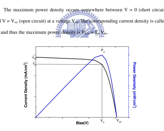
In general, the power delivered from a power source is P = IV, i.e. the product of voltage and current. If we instead use the current density J, we get the power density:
JV
P
d=
(6) The maximum power density occurs somewhere between V = 0 (short circuit) and V = Voc (open circuit) at a voltage Vm. The corresponding current density is called Jm, and thus the maximum power density is Pd,m = Jm Vm.
Bias(V) C u rr e n t D e n s it y ( m A /c m 2 ) Pm JSC VOC J m Vm P o w e r D e s n is ty (m W /c m 2 )
Figure 1.3: J~V characteristics and Maximum power
The efficiency of a solar cell is defined as the power (density) output divided by the power (density) output. If the incoming light has a power density Ps, the
efficiency will be
s m m
P
V
J
=
η
(7)
The fill factor, FF, is another quantity which is used to characterize a solar cell. It is defined as OC SC m m
V
J
V
J
FF
=
(8)and gives a measure of how much of the open circuit voltage and short circuit current is "utilized" at maximum power. Using FF we can express the efficiency as
s OC SC
P
FF
V
J
=
η
(9)
The four quantities Jsc, Voc, FF and η are frequently used to characterize the performance of a solar cell. They are often measured under standard lighting conditions, which implies Air Mass 1.5 spectrum, light flux of 1000W/m2 and temperature of 25°C.
1.2.3 Natural Limits of Efficiency
In addition to optimizing the production processes, work is also being done to increase the level of efficiency, in order to lower the costs of solar cells. However, different loss mechanisms are setting limits on these plans. Basically, the different semiconductor materials or combinations are suited only for specific spectral ranges. Therefore a specific portion of the radiant energy cannot be used, because the light quanta (photons) do not have enough energy to "activate" the charge carriers. On the other hand, a certain amount of surplus photon energy is transformed into heat rather than into electrical energy. In addition to that, there are optical losses, such as the shadowing of the cell surface through contact with the glass surface or reflection of
incoming rays on the cell surface. Other loss mechanisms are electrical resistance losses in the semiconductor and the connecting cable. The disrupting influence of material contamination, surface effects and crystal defects, however, are also significant. Single loss mechanisms (photons with too little energy are not absorbed, surplus photon energy is transformed into heat) cannot be further improved because of inherent physical limits imposed by the materials themselves. This leads to a theoretical maximum level of efficiency, i.e. approximately 28% for crystalline silicon.
Figure 1.4: Theoretical maximum levels of efficiency of various solar cells at standard conditions [51].
To maximise current density JPV it is necessary • maximise generation rate G • minimise recombination rate Generation rate is given by
(
x
)
x
dt
n
d
x
G
gen)
(
exp
)
(
)
(
)
(
)
;
(
)
(
)
(
)
;
(
0λ
α
λ
λ
β
λ
α
λ
λ
β
λ
α
λ
−
Φ
=
Φ
=
∆
=
(10) Where,φ
0=
φ
in(
1
−
R
)
(11)
Where, α is absorption co-efficient, φ is no of photons incident.
So from equation 10 and equation 11, it is seen that generation rate depends on the no of photons, absorption co-efficient, thickness of material, and reflection. So, to maximize generation rate it is necessary to minimize surface reflection, especially in the visible region of solar spectrum as shown in Figure 1.5.
Figure 1.5: Solar Spectrum [50].
Since, Silicon and III-V materials are generally used for high efficiency solar cell and these semiconductor materials have high refractive index [2]. As per Fresnel equation, there is over 30% of solar spectrum reflected by surface and energy is wasted. So, to improve the cell efficiency, we need to reduce reflection and increase
the absorption.
The methods to reduce reflection are: 1. Anti-reflection coatings
2.
Sub-wavelength Structures1.3 Antireflection Coatings
1.3.1 Single Layer Antireflection Coatings
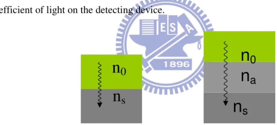
Anti reflective coatings (ARCs) are types of optical coating applied to lenses and other devices to reduce reflection from optical surfaces. It’s a popular strategy to place ARCs on light detecting devices to improve device quantum efficiency. Such coatings rely on destructive interference of reflected waves to reduce overall reflection coefficient of light on the detecting device.
Fig. 1.6: Schematic of different material structure (a) two layers without ARC (b) Three layers with ARC
A single layer coating on a substrate is shown in Fig. 1.6 (a). The refractive indices of the surrounding medium and the substrate are n0 and ns, respectively. Now suppose light falls from top and passes through the two medium. Then from the Fresnel’s principle the fraction of photons reflected at the interface between two medium with different refractive indices is given by
n
s
n
a
n
0
n
0
2 0 0 + − = n n n n R s s
(11) Silicon’s high index of refraction varies from n = 3.5 at 1.1 µm (infrared) to n = 5.6 at 0.4 µm (violet), and produces a large reflection coefficient across the solar spectrum: 34 % at 1.1µm increasing to 54 % at 0.4 µm. Any mechanism that increases the coupling of light in to the silicon surface improves the short-circuit current of silicon solar cell. There are two approaches: texturing of the surface to produce multiple reflections back into the silicon and creation of matching section (ARCs) to lower the reflection coefficient.
Now let’s use another layer3 as ARC with refractive index na in between layer1 and layer2 as shown in figure 1.6 (b). Now the equation (1.6) will become
(
)
(
)
2 2 0 2 0 + − = a s a s n n n n n n R(12)
The necessary and sufficient conditions for a single-layer coating to produce zero reflectance are:
na = (n0ns)1/2, na < ns (13) and
n
ad
4
λ
=
(14) Where d is the antireflection layer thickness and λ is the wavelength of the incident light.From equation (14) the optical thickness nad is then one quarter wavelength of the incident light. This antireflection coating is known as a quarter-wave coating. The reflectance of quarter wave coating is equal to zero at the wavelength corresponding
to optical thickness of quarter wavelength, if equation (13) is satisfied. If equation (13) is not satisfied, then the reflectance will indicate a minimum at the same wavelength.
The position of the reflectance minimum of a surface coated with a quarter-wave coating depends on the optical thickness of the coating and shifts towards longer wavelengths as the optical thickness increases. The effectiveness of a single-layer antireflection coating is limited by the available materials with suitable index.
Moreover, zero or minimum reflectance can be obtained at only one wavelength and the reflectance increases rapidly on both side of the zero or minimum position. Several transparent and high refractive-index material films have already been applied to ARC techniques, e.g. SiO (n=1.8–1.9), SiO2 (n=1.44), Si3N4 (n=1.9), TiO2 (n=2.3), Al2O3 (n=1.86), Ta2O5 (n=2.26), and SiO2–TiO2 (n=1.8–1.96) [3-8].
For application of high efficiency solar cell, we always demand a broadband and Omni directional antireflection layer [9]. These difficulties can be largely overcome by using coatings with two or more layers.
1.3.2 Multi-layer Antireflection Coatings
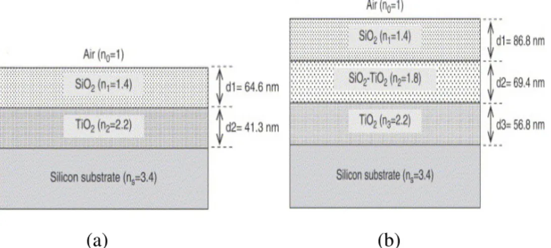
Multiple layers are more effective over the entire visible spectrum. For the double-layer ARC design, the low–high index on the Si substrate (i.e., the outer layer has the low refractive index and inner layer has high refractive index) is used. Figure 1.7 (a) and (b) show the typical double and triple layer antireflection coatings structure [Multilayer]. The principle of this type of ARC has been illustrated using the vector methods previously [10-12].
(a) (b)
Figure 1.7 Diagram of antireflection coatings with (a) SiO2/TiO2 double
layers and (b) SiO2/SiO2–TiO2/TiO2 triple layers.
Optical coatings are generally performed by vacuum processes such as thermal evaporation, reactive sputtering, and plasma-enhanced chemical vapor deposition (PECVD). All these methods are capable of producing films with uniform thickness and good optical properties. However, the conventional vacuum deposition processes are expensive and unsuitable for continuous mass production techniques in low-cost solar cells. So, these multilayer antireflection coatings (ARCs) are expensive to fabricate owing to the stringent requirement of high vacuum, material selection, and layer thickness control. Also additional problem of thermal mismatch between different layers and difficulties with the availability of materials with suitable optical properties arises in case of multilayer ARCs.
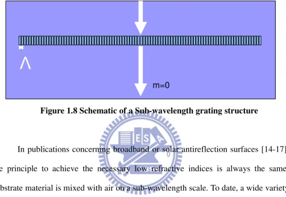
1.4 Sub-wavelength Structures
An alternative to multilayer ARCs is the sub-wavelength structures (SWS) surface with dimensions smaller than the wavelength of light. SWSs are zero order grating structures with the period of grating is much smaller than incident wavelength so that there will be only one reflected wave and one transmitted wave as shown in
Figure 1.8. Other high-order diffracted waves are forced to be evanescent. An electromagnetic wave propagates through a sub-wavelength or zero-order grating in approximately the same manner that it propagates through a homogeneous non-corrugated medium [13].
Figure 1.8 Schematic of a Sub-wavelength grating structure
In publications concerning broadband or solar antireflection surfaces [14-17], the principle to achieve the necessary low refractive indices is always the same: substrate material is mixed with air on a sub-wavelength scale. To date, a wide variety of techniques were examined for texturing microcrystalline-Si cells [18-21]. One of promising options is surface texturing by dry etching technique. Fabricating uniform textures with a submicron scale on mc-Si wafers by reactive ion etching (RIE) for Si solar cells [22-23] has been studied. But, this forms the dislocations and defects in the semiconductor layer. These defects and dislocations are responsible for increasing the minority carrier recombination in solar cell. Thus, the short circuit current for the solar cell is decreased, which in turn decreases the efficiency of solar cell.
1.5 Motivation
Therefore, key issues need to be solved: m=0
(1) It is necessary to find a way to form the sub-wavelength structure which can reduce reflectance and reduce the damage created by RIE method.
(2) It is necessary to find the way to replace the deposition of second ARC layer so that we can low down the cost of deposition of another layer and thermal mismatch.
(3) It is necessary to develop a low cost and easy fabrication method to form the sub-wavelength structure on antireflection coating.
Therefore, we studied the possibility of sub-wavelength structure on ARC surface instead of semiconductor surface, which may benefit the Si solar cell technologies. We chose to study the silicon nitride (Si3N4) sub-wavelength structure for this study due to the following reasons:
(1) Si3N4 is a well-known ARC used in semiconductor industry. (2) No previous studies about solar cell with Si3N4 SWS.
(3) Sub-wavelength structures will act as a second ARC layer with an effective refractive index so that the total structure can perform as a double layer antireflection layer (DLAR) layer.
(4) Si3N4 SWS will avoid or reduce the problem of defects created in Si and will improve the efficiency of Solar Cell.
In this work, we calculate the spectral reflectivity of pyramid-shaped Si3N4 sub-wavelength structures (SWS). A multilayer rigorous coupled-wave approach is advanced to investigate the reflection properties of Si3N4 SWS. We examine the simulation results for single layer antireflection (SLAR) and DLAR coatings with SWS on Si3N4 surface, taking into account effective reflectivity over a range of
wavelengths and solar efficiency. Also we compare the pyramid-shaped structures with cone, parabola, and cylinder-shaped SWS to see the effect of shapes on reflectance property of SWS.
Based upon our theoretical observation efficiency of silicon solar cell with silicon nitride SWS, we develop a simple and scalable approach for fabricating sub-wavelength structures (SWS) on silicon nitride by means of self-assembled nickel nano particle masks and inductively coupled plasma (ICP) ion etching. The size and density of nickel nano particles is optimized by considering different parameters.
Nevertheless, the surface profile of a sub-wavelength structure is strongly dependent on the conditions of the RIE process. So, we investigate the effect of ICP etching conditions on the profile of fabricated sub-wavelength structure on Silicon nitride antireflection coating layers.
1.6 Thesis content
The introduction to solar cell, the need of sub-wavelength structure and the motivation for this work has been described in chapter 1.
In chapter 2, the theory and design of sub-wavelength structure developed in our work has been described. Modeling of sub-wavelength structures via effective medium theories is examined. Also, we will describe about PC1D calculation method of solar cell characteristics and the results in this chapter.
A detail description of our developed fabrication method and results for silicon nitride sub-wavelength structure is given in chapter 3. Furthermore, the description of the instruments used in process and measurement are given in this chapter.
In chapter 4, the fabrication methods of silicon nitride nanocone structures are described with detail fabrication mechanism. Also the results are analyzed in the chapter.
In chapter 5, we will describe the results of fabricated solar cell using silicon nitride sub-wavelength structures in briefly.
Then, in the final chapter, we will summarize and conclude our studies and findings. Some suggestions for future studies will also be given for the improvement of the silicon nitride sub-wavelength structures.
Chapter 2
Design and Simulation of Silicon Nitride SWS
It is necessary to study the reflectance properties of the silicon nitride sub-wavelength structures on silicon substrate with different shapes and optimize the structure height for the better average reflectance before studying the sub-wavelength structures experimentally. So in this chapter, the theory of the developed model for the study of sub-wavelength structures has been described in details with the results and their discussions. Also the procedure of electrical characteristics calculation of a silicon solar cell using the sub-wavelength structure and the results has been reported in this chapter.
2. 1 Sub-wavelength structure design
2.1.1 Theory and Simulation Procedure
For the simplicity, a single pyramidal structure, shown in Fig. 2.1(a), is explored for the reflectance property with respect to the wavelength. The region with brown color of SWS is Si3N4, the region with sky color stands for Si substrate, and the environment of the triangular part is air. The etched Si3N4 (i.e., the height of triangular part) is h and the thickness of the non-etched Si3N4 is s, both of these two parameters are designing parameters for the reflectance optimization.
The studied SWS is a diffractive structure and its reflectance property could be calculated by a rigorous coupled-wave analysis (RCWA) technique. RCWA is an exact solution of Maxwell’s equations for the electromagnetic diffraction by grating structures. A multilayer RCWA method is used in this study, where the effective medium theory (EMT) [24-26] is adopted to calculate the effective refractive index
for each partitioned uniform homogeneous layer, as shown in Fig. 2.1(b).
Figure 2.1: (a) Geometry of sub-wavelength structure studied in this work, where h is the height and s is the non-etched part of SWS. (b) A stack of uniform
homogeneous layers resulting from the partitioned geometry of (a) for the reflection calculation using the multilayer RCWA method and EMT.
Simplifications of Maxwell’s equations are based on the following assumptions: 1. Incident field is an arbitrary linearly polarized monochromatic plane
wave
2. Electromagnetic fields are time-harmonic 3. Media are linear, homogeneous and isotropic
4. Gratings are infinitely periodic and are approximated with a layered structure
Reducing the computational domain to one unit-cell, without loss of generality (WLOG), we first divide the pyramidal structure into several horizontal layers with equal thickness. As shown in Fig. 2.1(b), for each discreted position zl along the z direction, EMT implies that the effective refractive index n(zl) of each layer is approximated by
[
]
[
(
)
]
(
)
[
2]
2 2 2 ) ( 1 ) ( 2 ) ( 1 ) ( ) ( 1 ) ( SiN l l SiN SiN l l SiN l l n z f z f n n z f z f n z f z n − + + − + + − = , (15)where, f(zl) is the fraction of Si3N4 contained in each layer and is given by,
2 2
3
4
)
(
D
r
z
f
l l=
(16)rl is the base width for each layer and is given by
1
l lz
r
r
h
=
−
(17)and D is the base width of the structure,
n
SiN=
n
+
ik
is the complexrefractive index of Si3N4, i= −1, n and k are optical constants, and nair = 1 is the refractive index of air. Note that only the real part of refractive index of Si3N4 is considered in our simulation because it is weakly absorbing material [27]. With the calculated effective refractive index n(zl) for each layer, we can solve the reflectance property of the entire structure including a layer for the non-etched Si3N4 with respect
to the different wavelength.
From the partitioned structure, shown in Fig. 2.1(b), we now consider the reflection and the transmission of a transverse electric (TE) polarized plane wave of free-space wavelength λ, incident at angle θ, on L uniform layers of effective refractive indices nl = n(z1), …, nl, …, nL = n(zL) and thickness d1, …, dl, …, dL. For each layer, the normalized electric field (in the x-y plane) for the input and the output regions is given by, for the air region, i.e., z≤0
x ik z ik z ik x z air z air
R
e
e
e
E
=
(
− ,+
×
− ,)
− 0 , (18)for the region of SWS, i.e.,
D
l−1≤
z
≤
D
l,x ik D z ik l D z ik l l x l l l l
Q
e
e
e
p
E
=
(
×
− 0γ ( − −1)+
×
0γ ( − ))
− , (19) and for the Si substrate, i.e.,z
≥
D
L,)) ( (kxx kSi,z z DL i t
T
e
E
=
×
− + − , (20) Where,θ
sin
0 air xk
n
k
=
, (21)θ
cos
0 ,z air airk
n
k
=
, (22)θ
2 2 2 0 ,z Si airsin
Sik
n
n
k
=
−
, (23)θ
γ
2 2 2sin
air l l=
i
n
−
n
, (24)∑
==
l p p ld
D
1 , (25)l = 1, …, L, I, R and T are the incident, reflected and the transmitted amplitudes of the
is the wave-vector magnitude, and nair and nSi are the refractive indices of the air and
the silicon regions. Note that now the layer of non-etched Si3N4 has been added into
our simulation structure, where its effective refractive index nSiN = 2.05 is the same
with the original one and f(zL) = 1. The reflected and transmitted amplitudes of the
explored SWS are calculated by matching the tangential electric- and magnetic-field
components at the boundaries among layers [28]. First, for the boundary between the
input air region and the first layer of Si3N4 (i.e., z = 0), we have
×
−
=
−
×
+
=
+
− −)
(
)
1
(
1
1 1 0 1 1 0 1 1 1 0 , 1 1 d k z air d ke
Q
P
R
k
k
i
e
Q
P
R
γ γγ
. (26)For the boundary between the (l - 1)st and the lth layers (i.e., z = Dl-1)
×
−
=
−
×
×
+
=
+
×
− − − − − − − − − − − − −)
(
)
(
0 1 1 0 0 1 1 0 1 1 1 1 1 l l l l l l l l d k l l l l d k l l d k l l l d k le
Q
P
Q
e
P
e
Q
P
Q
e
P
γ γ γ γγ
γ
; (27)for the boundary between the last layer and the output Si region (i.e., z = DL), the
matched equations are
=
−
×
=
+
×
− −T
k
k
i
Q
e
P
T
Q
e
P
z Si L d k L L L d k L L L L L)
(
)
(
0 , 0 0 γ γγ
. (28)The equations (26)-(28) could be solved by using a transmittance matrix method [29].
Using Eq. (28), the field amplitudes PL and QL in terms of the transmitted coefficient
amplitudes PL-1 and QL-1. Consequently, the system of equations to be solved for the
reflection properties is given by
T
k
k
i
e
e
e
e
R
k
k
i
k
k
i
Siz l d k l d k L l d k l l d k z air z air l l l l l l l l
×
−
×
−
=
−
+
− − − = − −∏
0 , 1 1 0 , 0 ,1
1
1
1
1
0 0 0 0γ
γ
γ
γ
γ γ γ γ ,(29)for partitioned layers of SWS. Similarly, a set of governing equations could be
derived for the transverse magnetic (TM) polarization. Here the incident angle θ of
sun light is assumed to be normal to the plane (i.e., θ = 0ο), and only the TE polarization is considered here for the calculation of the reflection properties [30].
For a given number of layers for the SWS including the layer of non-etched
Si3N4, say L in total; a calculation procedure for computing the reflectance properties
of the studied SWS described above is summarized: (i) calculate the effective
refractive index for each zl via Eq. (1); (ii) compute the coefficients using Eqs.
(21)-(25) for a specified wavelength λ; (iii) and solve Eq. (29) to get the unknowns R
and T.
2.1.2 Results and Discussions
First of all, we compare the reflectance with respect to the wavelength of
sunlight for the SWS with Si and Si3N4. As shown in Figure 2.2(a), by assuming a
versus the wavelength for Si SWS with h = 88 nm and Si3N4 SWS with h = 88 nm and
vanished non-etched part of SWS (i.e., s = 0 nm) is simulated and compared.
(a)
Wavelength (nm) 400 500 600 700 800 900 1000 R e fl e c ta n c e ( % ) 5 10 15 20 25 30 35 Si SWS w/ h = 88 nm Si3N4 SWS w/ h = 68 nm and s = 20 nm Si3N4 SWS w/ h = 88 nm(b)
Figure 2.2: (a) The schematic of Si and Si3N4 SWS for the study. (b) The
with h = 88 nm and vanished non-etched part of SWS (i.e., s = 0 nm). Comparison for the Si3N4 SWS with the case of non-zero s, say s = 20 nm is also
provided. It is found that it is possible to reduce the reflectance of Si3N4 SWS by
proper selection of h and s.
As seen from Figure 2.2(b), it is found that the non-optimized Si3N4 SWS
possesses a little bit higher reflectance which may not be a plus for ARC. However,
we can design a Si3N4 SWS with the case of non-zero s, say h = 68 nm and s = 20 nm,
which shows that the reflectance is close to the result of Si SWS or even better. This
observation motivates us to explore the morphology-dependent reflectance of Si3N4
SWS with a set of optimized h and s. Note that Si refractive index nSi may depend
upon the wavelength of incident sunlight [31]; our calculation for the Si3N4 SWS with
h = 68 nm and s = 20 nm confirms the reflectance difference between the model with
constant and wavelength-dependent nSi, as shown in Figure 2.3. In this calculation, an
empirically fitted formula for the wavelength-dependent nSi is implemented in our
simulation program [32]
(
2)
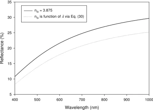
1 2 2 1 2 λ λ λ λ ε − + + = A B nSi , (30) where, λ1 =1.1071µm, ε = 11.6858, A = 0.939816µm2 and B = 8.10461 × 10⁻³.Wavelength (nm) 400 500 600 700 800 900 1000 R e fl e c ta n c e ( % ) 5 10 15 20 25 30 35 nSi = 3.875
nSi is function of λ via Eq. (30)
Figure 2.3: The spectral reflectivity of Si3N4 SWS for h = 68 nm and s = 20
nm with constant Si refractive index and refractive index as a function of lambda given by Eq. (28).
Using the above empirical fitted formula, the refractive index of silicon is plotted
for wavelength from 400 nm to 1000 nm as shown in Figure 2.4.
Instead of considering the reflectance for a certain wavelength, an effective
reflectance is further computed for the structures over a range of the wavelength of
incident sunlight. By taking purely Si in the SWS part of Figure 2.1(a), where s = 0
nm and h is designed as a varying factor, we now calculate the effective reflectance
Reff [33] for the wavelength λ varying from λl = 400 nm to λu =1000 nm and compare
it with Si3N4 SWS. Reff is evaluated by
∫
∫
= u l u l d E SI d E SI R Reff λ λ λ λ λ λ λ λ λ λ λ ) ( ) ( ) ( ) ( ) ( , (31) where, SI(λ)is spectral irradiance given by ATMG173 AM1.5G reference [34],E(λ) is photon energy and R(λ) is the calculated reflection.
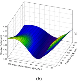
Height of Si SWS (nm) 0 100 200 300 400 E ff e c ti v e R e fl e c ta n c e 0.00 0.05 0.10 0.15 0.20 0.25 0.30 0.35
(a)
0.00 0.05 0.10 0.15 0.20 0.25 0.30 0.35 20 40 60 80 100 120 140 160 180 200 20 40 60 80 100 120 140 160 180 E ff e c ti v e R e fl e c ta n c e Hei ght o f Si3 N4 ( nm ) Thickness o f non-etched Si3N4 (nm) (b)
(b)
Figure 2.5: The effective reflectance for the wavelength varying from 400 nm to 1000 nm; plot is as a function of (a) h for Si SWS and (b) of h and s for
Si3N4 SWS.
Figures 2.5(a) and 2.5(b) show the effective reflectance as a function of h for Si
SWS, and of h and s for Si3N4 SWS. For Si SWS, there is a minimum Reff = 3.89% for
h = 220 nm, and for Si3N4 SWS, the minimum of Reff = 3.43% occurs at h = 150 nm
and s = 70 nm. Compared with Si SWS, the improvement of Reff for Si3N4 SWS is due
to the nature of Si3N4 and an optimal combination of the height of etched part of Si3N4
and the thickness of non-etched part of Si3N4.
It has been reported that SLAR and DLAR were used in solar cell, for a unified
comparison; similarly, we further examine their Reff over the same wavelength, as
(a)
(b)
Figure 2.6: Plot of the effective reflectance for the wavelength varying from 400 nm to 1000 nm. (a) is the result as a function of the thickness of Si3N4 ARC
with n = 2.05for SLAR coating on Si. (b) is the result as a function of the thickness of ARC 2 and refractive index of ARC 2 for Si3N4 / ARC 2 DLAR
coating on Si. The thickness of Si3N4 ARC 1 is fixed at 80 nm which is optimized
from (a).
For Si3N4 SLAR coating on Si, as shown in the inset of Figure 2.6(a), the
refractive index is equal to 2.05, where the thickness of ARC is varied. For Si3N4 /
ARC 2 DLAR coating on Si, the thickness of ARC 2 and the refractive index of ARC
2 are varied. Note that the thickness of ARC 1 equals 80 nm, as shown in the inset of
Figure 2.6(b), directly comes from the optimal value of Figure 2.6(a), and the lower
bound of refractive index of ARC 2 starts from 1.38 which is the refractive index of
MgF2. The lowest Reff occurs when the refractive index of ARC 2 is 1.38 and its
thickness is 100 nm.
Based upon the investigation of Figs. 2.5 and 2.6, we show the optimal
reflectance spectra among the bulk Si (i.e., the bare Si), the optimized SLAR, DLAR,
Wavelength (nm) 400 500 600 700 800 900 1000 R e fl e c ta n c e ( % ) 0 10 20 30 40 50 60 Bare Si Si SWS w/ h = 220 nm Si3N4 SWS w/ h = 150 nm and s = 70 nm SLAR, thickness of Si3N4 = 80 nm
DLAR, thickness of ARC 1 and ARC2 is 80 nm and 100 nm
Figure 2.7: Comparison of the reflectance spectra among the bulk Si (i.e., the bare Si), the optimized SLAR, DLAR, Si SWS and Si3N4 SWS for the
wavelength from 400 nm to 1000 nm.
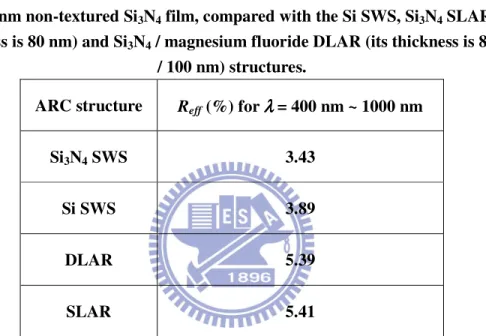
Table 1 lists the effective reflectivity for those optimized structures of 150 nm Si3N4
SWS and 70 nm non-textured Si3N4 film, compared with the Si SWS, Si3N4 SLAR
(its thickness is 80 nm) and Si3N4 / MgF2 DLAR (its thickness is 80 nm / 100 nm)
structures. The flat silicon substrate exhibits high reflection > 35% for visible and
near infrared wavelengths, Si3N4 SLAR coatings exhibits low reflection < 20% for
long wavelengths 700 nm and high reflection > 35% for shorter wavelengths 400 nm,
and Si3N4 / MgF2 DLAR coatings exhibits low reflection < 10% for long wavelengths
gratings show reduced reflection of < 10% for whole wavelengths. The Si3N4 SWS
with h = 150 nm and s = 70 nm exhibits lowest effective reflectivity among five
structures; consequently, the optimized morphology of Si3N4 SWS could be a
promising alternative for DLAR in Si solar cell technology.
Table 1. Effective reflectivity for those optimized structures of 150 nm Si3N4 SWS
and 70 nm non-textured Si3N4 film, compared with the Si SWS, Si3N4 SLAR (its
thickness is 80 nm) and Si3N4 / magnesium fluoride DLAR (its thickness is 80 nm
/ 100 nm) structures.
ARC structure Reff (%) for λλλλ = 400 nm ~ 1000 nm
Si3N4 SWS 3.43 Si SWS 3.89 DLAR 5.39 SLAR 5.41
2.2 Shape Effect
2.2.1 Simulation Procedure
The shape of the SWS may be somewhat variable and, therefore, we performed
reflectance calculations for a few model shapes, a cone, paraboloid and cylindrical,
The RCWA model as described in section 2.1 was used to calculate the reflectance
of the three types of shapes for normally incident light. Therefore, for a cone shape, the
equation (16) and (17) will become
( )
2 23
l lr
f z
D
π
=
(32)1
l lz
r
r
h
=
−
(33)Figure 2.8: Three model shape types (a) cone (b) parabola and (c) cylinder shape.
Similarly, for paraboloid and cylindrical shape, the fraction of Si3N4 layer and
( )
2 23
1
l l l lr
f z
D
z
r
r
h
π
=
=
−
(34)( )
2 23
l l lr
f z
D
r
r
π
=
=
(35)2.2.2 Results and Discussion
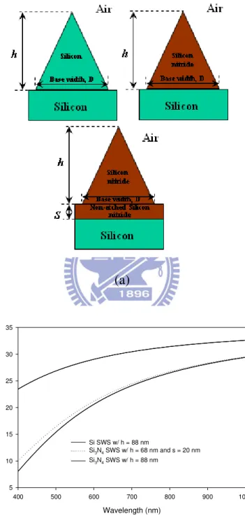
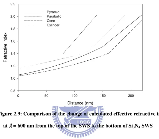
The calculated effective refractive index at λ = 600 nm from the top of the SWS to the bottom of Si3N4 SWS for the four shapes (i.e. Pyramid, parabolic, cone and cylinder) in our simulation is shown in Fig.2.9.
The graded index, which is desirable for suppressing the optical reflection, [35] is
observed for pyramid, cone and parabolic shapes—the refractive index changes from
1.0 to 1.5 for pyramid, from 1.0 to 1.4 for cone and from 1.0 to 1.4 at the air/silicon
nitride interface and then changes sharply to the bulk index of silicon nitride. But for a
cylinder shaped SWS, the effective refractive index calculated is 1.4. From the
comparison, it is found that the slope of the change of refractive index is lowest for
cone shaped SWS. Using microwave models, experimentally it has been demonstrated
that the strong reflectance reduction by a nipple array with cone-shaped nipples [36].
to pyramid or parabolic or cylinder shaped SWS. The optimizations of the structures
and the comparison results will be discussed next.
Distance (nm) 0 50 100 150 200 R e fr a c ti v e I n d e x 0.8 1.0 1.2 1.4 1.6 1.8 2.0 2.2 Pyramid Parabolic Cone Cylinder
Figure 2.9: Comparison of the change of calculated effective refractive index at λλλ = 600 nm from the top of the SWS to the bottom of Siλ 3N4 SWS
Similarly, as we varied the “s” and “h” for pyramid structure, we varied the these
two parameters for parabola, cone and cylindrical shapes to see the lowest effective
reflectance and the optimization results are shown in Fig. 2.10, Fig. 2.11 and Fig. 2.12,
respectively. The reflectance spectra of the optimized structures are compared in Fig.
2.13. The lowest effective reflectance of 3.14% has been seen for the optimized cone
0.00 0.05 0.10 0.15 0.20 0.25 0.30 0.35 20 40 6080 100120 140160 180200 20 40 60 80 100 120 140 160 180 E ff e c ti v e R e fl e c ta n c e Hei ght o f S i 3N 4 SW S ( nm ) Non-Etched Pa rt of Si3N4 (nm) 0.00 0.05 0.10 0.15 0.20 0.25 0.30 0.35
Figure 2.10: Parabola Shape optimization
0.00 0.05 0.10 0.15 0.20 0.25 0.30 0.35 20 40 60 80 100120 140160 180200 20 40 60 80 100 120 140 160 180 E ff e c ti v e R e fl e c ta n c e Hei ght o f Si3 N4 S WS (nm ) Non-Etc hed Part of Si 3N4 (nm) 0.00 0.05 0.10 0.15 0.20 0.25 0.30 0.35
0.00 0.05 0.10 0.15 0.20 0.25 0.30 0.35 20 40 60 80 100 120140 160180 200 20 40 60 80 100 120 140 160 180 E ff e c ti v e R e fl e c ta n c e Hei ght o f Si3 N4 S WS (nm )
Non-Etched Part
of Si3N4 (nm) 0.00 0.05 0.10 0.15 0.20 0.25 0.30 0.35
Figure 2.12: Cylinder shape optimization
Wavelength (nm) 400 500 600 700 800 900 1000 R e fl e c ta n c e ( % ) 0 2 4 6 8 10 12 14 Parabola w / h = 130 nm & s = 70 nm Reff = 3.24 % Cone w / h = 160 nm & s = 70 nm Reff = 3.15 % Pyramid w / h = 150 nm & s = 70 nm Reff = 3.43 % Cylinder w / h = 70 nm & s = 60 nm Reff = 4.25 %
Figure 2.13: Comparison of optimized structures with different shape But, the comparison of the reflectance spectra of the four shapes as shown in Fig.
2.13 may not be correct as the volumes of the different shapes are different. For this
![Figure 1.4: Theoretical maximum levels of efficiency of various solar cells at standard conditions [51]](https://thumb-ap.123doks.com/thumbv2/9libinfo/8612526.190818/23.918.220.704.453.816/figure-theoretical-maximum-levels-efficiency-various-standard-conditions.webp)