A
國 立 交 通 大 學
奈 米 科 技 研 究 所
碩 士 論 文
新穎背向閘極奈米線場效電晶體結合自組裝單分子層於即時偵測肝
癌生物標記感測器之應用與探討
Real-Time and Label-Free Detection of the Cancer Maker of
Hepa-tocyte Tumor by a Novel Back-gated SiNB-FET Biosensor.
研究生: 李柏軒 Bo-Syuan Lee
學號: 9652509
指導教授: 柯富祥 博士 Dr. Fu-Hsiang Ko
B
新穎背向閘極奈米帶場效電晶體結合自組裝單分子層於
即時偵測肝癌生物標記感測器之應用與探討
Real-Time and Label-Free Detection of the Cancer Maker of
Hepa-tocyte Tumor by a Novel Back-gated SiNB-FET Biosensor.
研究生: 李柏軒 Bo-Syuan Lee
指導教授: 柯富祥 博士 Dr. Fu-Hsiang Ko
國立交通大學
奈米科技研究所
碩士論文
A ThesisSubmitted to Institute of Nanotecnology College of Engineering
National Chiao Tung University in Partial Fulfillment of the Requirements
for the degree of Master in Nanotechnology
July 2009
Hsinchu, Taiwan, Republic of China
i
Acknowledgment
這兩年的碩班生活,首先要感謝的當然是柯富祥博士。因為柯老師總是會 為學生著想,也總是支持著學生的理想,學術上對我提供的幫助自然更不在話 下。這段時間能讓我在專業領域與待人處事上跨進一大步,是因為有老師您。 再來,要感謝其昌學長在實驗上實質與精神上的幫忙!這兩年來,謝謝你 提供不管是在元件上,或知識上的支援,真不敢想像如果沒有你在,我的碩士 論文會是甚麼模樣。我超崇拜你的,你是真男人!再來我想要謝謝中書學長, 嘖嘖,實驗室生物相關的問題我好像只能問同背景的你,也謝謝你熱心的跟我 討論,還無私的教我奈米金的製備與應用,雖然最後好像都沒用到哈哈哈。我 也感謝一開始帶我實驗的皮皮學姊,謝謝妳一開始給我的啟蒙,不然我還真不 知實驗要從哪做起。再謝謝桃子學姐,之前我碩一甚麼都不懂所以問了很多蠢 問題,不過你還是有問必答,實在是非常的有耐心。謝謝強者我同學林京璋, 除了偶爾跟你討論實驗獲得的寶貴靈感外,最重要的是我們在某大型多人3D 立體技術交流平台上一起奮鬥的日子,諸如團隊合作,與責任感,我想我學到 了很多,祝你早生貴子。謝謝鄭捷,一個曖曖內含光的帥哥,謝謝你提供實驗 室區域連線多媒體,讓實驗室隨時都充滿著挑戰與歡樂,而且還開車帶我們環 校觀光,吃晚餐。謝謝一點都不像雙子座的馮玟菲,謝謝妳提供的肝細胞,我 也一直很欣賞妳的行事風格,哈。謝謝何嘉琦,祝妳減肥成功,雖然你一點都 不胖阿。。。實驗與論文方面,我相信妳一定沒問題啦,絕對可以早早畢業! 蘇丁香,謝謝你在實驗上給我的支持與幫助,現在想想,如果沒有妳提供的笑 點,在實驗不順利時其實是非常的悶阿!還有加油喔,很遺憾畢業後在實驗方 面沒辦法繼續支持妳,不過 我知道妳一定行的,明年就換妳畢業了。佳典學長, 你講的笑話我一直都覺得很好笑,哈。小朱學長,謝謝你不厭其煩的幫我設定 機台,和解決一些實驗室的疑難雜症。品麟學長,還記得我們在NDL奮鬥的 日子嗎?那段時間你也教導了我許多機台相關的知識。貞治同學,雖然我們有 時候會搶機台,不過我也要感謝你在NDL陪我做實驗,和幫我訂便當XD。 當然還要謝謝實驗室其他在不同領域中共同努力及患難與共的夥伴們:俊淇學 長,3.com 學長,Jagon 學長,宜生學長,美榕學姐,易成(一直跟我借刷子), 懷箴,崇志,品樺。因為有你們,讓我碩士生活平添了許多色彩。 最後我要感謝我的父母,兄弟姊妹,這兩年來給我的關心與包容,讓我能 隨時準備好面對挑戰。家住在台南,在新竹讀書卻沒能常常回家實在非常汗顏。 我會再持續進步,直到我有能力讓你們過著更好的生活,報答你們的養育與教 導之恩。。。 謹以此文 獻給我身邊的你們ii
新穎背向閘極奈米帶場效電晶體結合自組裝單分子層於
即時偵測肝癌生物標記感測器之應用與探討
學生: 李柏軒 指導教授: 柯富祥 教授
國立交通大學奈米科技研究所碩士班
摘 要
場效電晶體元件與生物分子偵測的連結應用在未來的疾病診斷與防治是個 重要且具發展淺力的新興科技。在此篇論文中,我們選擇血液酸鹼值,B 型肝 炎病毒 X 基因的去氧核醣核酸(DNA)片段序列與甲型胎兒蛋白(alpha feto-protein)抗原來當作偵測肝炎,肝硬化,與肝腫瘤的指標。我們以奈米米帶場 效電晶體(nanobelt field effect transsitor)為元件基礎的裝置,做為即時 偵測、不需外加標定、高靈敏度以及高特異性結合的生物感測器,可偵測的生 物分子或是化學物種包括有低濃度化學成分離子、小分子、抗原抗體反應、去 氧核醣核酸片段與檢測蛋白質。在我們的研究裡,使用了互補式金氧半場效電 晶體的技術來製作新穎背向閘極奈米帶場效電晶體生物感測器。利用矽的局部 氧化製程(LOCOS)來製作內縮線寬的奈米帶,而此奈米帶可以達到優異的高比表 面積比以及獲得背向閘極控制,此兩項主要特色對於目前感測元件整合於微流 道組件上有極大優勢及應用面潛力。我們量測血液酸鹼值、B 型肝炎病毒 X 基 因的去氧核醣核酸片段序列以及癌症指標物甲型胎兒蛋白抗原對於場效奈米帶iii 元件的電性變化影響,另外還利用了原子力顯微鏡、螢光顯微鏡以及電子顯微 鏡量測儀確認表面自組裝固定化的技術以及生物分子實驗條件的確立。 最後總結出我們利用矽的局部氧化製程製作出的奈米帶通道可使其線寬內 縮到 150 奈米以下的線寬,此條件提供元件電性達到優異的 105 倍的開關電流 比。利用此靈敏度高的元件我們可以偵測到接近濃度 1fM 的標的突變 DNA 以及 濃度為 3ng/mL(? 最靈敏應可作到很低)的癌症標誌物抗原分子。結果顯示此新 穎的背向閘極奈米線感測元件可以用作未來的免標定、即時偵測、高靈敏度以 及優異專一性結合的場效奈米帶電晶體生物感測器。另外,此元件具有控制背 向閘極的能力更提供了未來感測元件與微流道技術整合上的一大優勢。
iv
Real-Time and Label-Free Detection of the Cancer Maker of
Hepa-tocyte Tumor by a Novel Back-gated SiNB-FET Biosensor.
Student: Bo-Syuan Lee Advisor: Prof. Fu-Hsiang Ko
Institute of Nanotechnology National Chiao Tung University
Hsinchu 300, Taiwan, ROC
Abstract
The application of high-sensitive field-effect transistor devices in detecting the bio-molecules is an important and developing thchnology. The development of biological sensors could impact significantly the areas of genomics, proteomics, biomedical di-agnostics, and drug discovery in the future. In our thesis, the serum pH value, HBV X gene DNA fragments, and α-fetoprotein cancer marker were chosen as the target mo-lecules to detect the hepatocellular carcinoma. The devices based on semiconducter nanobelt exhibited highly sensitive and selective characteristics for the real-time, la-bel-free, and excellent specificity detection of biomolecules and chemical species. A novel back-gate silicon nanobelt field effect transistor (SiNB-FET) was fabricated by using the complementary metal oxide semiconductor (CMOS) compatible technology. The shrank nanobelt with high surface-to-volume ratio and individual back-gate were achieved by the local-oxidation of silicon (LOCOS) process. Because of the above advantages, the devices have potential to integrate with microfluidic system for bio-detection application. Therefore, the detection of hepatocellular carcinoma was investigated by measuring the characteristics of electrical signals. The atomic force microscopy (AFM)、fluorescence microscopy and scanning electron microscopy (SEM) were also examined to check out the self-assembly efficiency and appropriate experimental parameter for bio-sensing.
In conclusion, the width of nanobelt by LOCOS process can be shrank down to 150 nm. The drain current versus gate voltage (Id-Vg) characteristic of the
v
SiNB-FET exhibited about five orders of magnitude of Ion/Ioff current ratio, and the
threshold voltage shifts positively after hybridization of 1fM concentrations of HBV X gene DNA fragments and 3ng/mL concentrations of the cancer marker, anti-gen-α-AFP, respectively. The results show that the back-gated nanobelt device has the capability of acting as a real-time, label-free, highly sensitivity and excellent se-lectivity SiNB-FET biosensor in detecting biomolecules. Our approach offers the possibility of highly potential to integrate microfluidic-channel system for future parallel real-time detection of multiple chemical and biological species with control-ling the individual back-gate in a single integrated chip.
vi
Content
Acknowledgments………...…………i 摘要 (中文)……….………ii Abstract………...…………..iii Content……….…………..iv Chapter 1: Introduction………001 1.1 General Introduction……….…………0011.2 Top-Down and Bottom up………...…..…………003
1.2.1 Top-down method………...…..…..………003
1.2.2 Bottom-up method………..……….004
1.3 Employment of bioFET for ultra sensitive sensing………...…….006
1.4 Utilize the bioFET to diagnosis hepatocellular carcinoma (HCC)……....009
1.4.1. Detection the blood pH value………...009
1.4.2. Detection the blood alpha-fetoprotein (AFP)……….……..010
1.4.3 Detection the blood HBV X gene DNA fragments………..011
Chapter 2: Paper review………...015
2.1 Literature about self-assembled monolayer………..…….……015
vii
2.3 Real-time Nanobelt Field-Effect-Transisitor Biosensors……….……….028
Chapter 3: Experimental and material……….………033
3.0 Experimental process……….….033
3.1 Fabrication of back-gated silicon nanobelt field-effect transistor (NB FET)……….…..033
3.2 Self-assembly of APTES on the NBFET device for solu-tion pH detec-tion………..036
3.3 Self-assembly of capture DNA on the NBFET device…………....…..037
3.4 Self-assembly of antibody on the NBFET device……….…….039
3.5 Fluorescence labeled capture DNA……….……..040
3.6 PDMS sample channel fabrication……….……041
3.7 Assemble the FET sensor to the system………..………….……..042
3.8 Preparation of the pH degree solution………043
3.9 Preparation of the HBV X gene DNA fragments……….…..043
3.10 Preparation of the AFP sample in vitro or in vivo……….…..044
Chapter 4: Results and Discussion……….…..046
4.1 Physical and electrical properties of the back-gate SiNB-FET…….…046
viii
4.2.1 Hepatocellular carcinoma will cause blood acidosis cause……048
4.2.2 Detection response of the solution pH………..…048
4.2.3 Effect of the solution ion concentration to the NBFET……...050
4.3 Real-time detection of HBV x gene fragments……….……052
4.3.1 Certification of DNA immobilization by fluorescence image…...052
4.3.2 Effect of PBS to the bioFET DNA sensor………..…052
4.3.3 Real-time detection of X gene DNA fragments with various concentra-tions………..………..….053
4.3.4 Determination the sensing limit of bioFET DNA sansor…….…...054
4.3.5 Determination of the specificity sensing4.4 Real-time
detection of AFP cancer maker………055
4.4 Real-time detection of the liver cancer maker AFP………..…….058
4.4.1 Detection the different concentration AFP DNA fragments
sample solution………..….…..058
4.4.2 Detection the real mouse AFP level………..…060
4.4.3 Real-time detection of the AFP with various PBS concentrations.062
ix
4.5.1 Penetration of Na+ ions into the SOI wafer………064
4.5.2 Duration of APTES film on silicon oxide by AFM examination.065 4.5.3 Duration of DNA strand on silicon oxide………...……….066
4.5.4 The degeration mechanism of self-assembled APTES mono-layer on silicon oxide surface………068
Chapter 5: Conclusion………071 Reference……….073 Chapter 1 references………..073 Chapter 2 references………..074 Chapter 3 references………..077 Chapter 4 references………..078
List of Figures
Chapter 1: Introduction
Figure 1-1………..002 Diagram of nanotechnology. Figure 1-2………..004x
Schematic diagram of the top-down mwthod.
Figure1-3………005 Diagram of bottom up procedure.
Figure 1-4……….………..008
Diagram of biosensor.
Figure 1-5………...010
Secretion of the abnormal liver tumor.
Figure 1-6………...011
AFP secretion by abnormal liver.
Figure 1-7………012
The human hepatitis B virus gene map.
Figure 1-8……….…..013
IGF-II physiology pathway.
Figure 1-9……….………..013
p53 physiology path way.
Chapter 2: Paper review
Figure 2-1……….………..017
APTES films scan by three-by-three matrix AFM.
Figure 2-2……….…..017
Representative morphologies of APTES films.
Figure 2-3………...018
xi
Figure 2-4………019
Chemical mechanism of APTES coating.
Figure 2-5………..021
Field emission scanning electron microscopy photos of the fabricated devices.
Figure 2-6………...021
Gases responded by nanowire devices.
Figure 2-7………...022
Optical and SEM image of nanowire sensor.
Figure 2-8………..023
Optical and SEM image of nanowire sensor.
Figure 2-9………..024
SEM image of SiNW after reaction of the GNPs with APTMS.
Figure 2-10………024
ID-VG curves of SiNW after binding of different molecules on the surface of SiNW.
Figure 2-11………025
The 3-D AFM image of 40 nm width Pt-silicide nanowire, and the immobilization steps for the DNA on the Pt-silicide nanowire.
Figure 2-12……….026
Device fabrication and electrical performance.
Figure 2-13……….028
xii
Figure 2-14……….030
NW-FET sensors.
Figure 2-15………..031
NW arrays for multiplexed protein sensing.
Chapter 3: Experimental procedure
Figure 3-1………..035
Schematic Diagram of the NB FET fabrication process.
Figure 3-2………..036
Procedure of APTES immobilization on the NBFET surface.
Figure 3-3………..038
Procedure of DNA Immobilization on the NBFET surface.
Figure 3-4………..040
Procedure of antibody coated on SiNB.
Figure 3-5………..041
Procedure of FITC-DNA immobilized.
Figure 3-6………..042
Schematic diagram of the microfludic channel fabrication process.
Chapter 4: Result and Discussion
Figure 4-1………..047
SEM image of silicon nanobelt & Electrical properties of SiNB FET sensor.
Figure 4-2………..049
xiii
Figure 4-3………..050
Drain current of the NB FET sensor as a function of solution pH.
Figure 4-4………..051
Drain current of sensor as a function of PBS concentrations with various pH solution.
Figure 4-5………..052
Fluorescence image of the fluorescence-labeled DNA immobilized on the 60 nm-silicon nanobelt.
Figure 4-6………..053
Typical electrical response of PBS injection into the BioFET sensor.
Figure 4-7………..054
Electrical responses of HBV X gene DNA sample with various concentrations.
Figure 4-8………..055
Detection limit of the DNA sensor.
Figure 4-9………..057
Response of the mismatch DNA of the DNA sensor.
Figure 4-10………059
Detection response with various AFP concentrations from 3 to 600 ng/ml.
Figure 4-11………060
Normalized current shift as a function of AFP concentration.
xiv
Detecting response of AFP concentration from adult and infant mice.
Figure 4-13………..063
Influence of ion concentration of phosphate buffer in the real-time.
Figure 4-14………..065
Drain current shifts of the NB FET sensors as a function of PBS soaping days.
Figure 4-15………...066
AFM images of APTES self assembled monolayer after various soaping time.
Figure 4-16………068
Current shift of the modified NB FET sensor with soaping time.
Figure 4-17……….070
1
Chapter 1: Introduction
1.1 General introduction
Nanotechnology, which is sometimes shortened to "Nanotech", refers to a region whose study is the control of matter on an atomic and molecular scale. Nanotech-nology is also believed that is a important revolution about science, industry, and our life. A nanometer is one-billionth of a meter. A sheet of paper is about 100,000 nanometers thick; a single hydrogen atom is about a 1/10 nanometer in diameter. Nanoscale means something diameter is about 1 to 100 nanometers. Under the na-noscale level, different physical, chemical, and biological properties could emerge. These properties may bring the diverse important application way from the proper-ties of bulk materials and single atoms or molecules.
Generally, nanotechnology is definition as a skill that to handles structures of the size 100 nanometers or smaller, study and technology development at the atomic, molecular or macromolecular scales, to provide a fundamental understanding of phenomena and materials at the nanoscale and to create and applied structures, de-vices and systems that have novel properties and functions because of their small and/or intermediate size.
The first use of the concepts in 'nano-technology' (but predating use of that name) was in "There's Plenty of Room at the Bottom," a talk given by physicist Richard Feynman at an American Physical Society meeting at Caltech on December 29, 1959. The benifit of nanotechnology is rooted in its potential to transform and
revo-2
lutionize multiple technology and industry sectors, including aerospace, agriculture, biotechnology, homeland security and national defense, energy, environmental im-provement, information technology, medicine, and transportation.
Nanotechnology is going to change the world and the way we live, creating new scientific applications that are smaller, faster, stronger, safer and more reliable.
Figure 1 is the diagram of nanotechnology, the nanotechnology is belong in the mesososmic region, in this size many material will result somewhat new property, Created and applied structures, devices and systems that have novel properties and functions cause by their small and/or intermediate size.
Fig. 1-1 Diagram of nanotechnology. Nanotechnology is technology development
3
devices and systems that have novel properties and functions cause by their small and/or intermediate size.
1.2 Top-down and bottom-up
There are two groups of researcher with opposing approaches to nanotechnology utilization will meet and find a middle ground. The two camps are informally re-ferred to as "top-down" and "bottom-up"[1]. Top-down methods start with patterns made on a large scale and reduce its lateral dimensions before forming nanostruc-tures. On the other hand, bottom-up methods begin with atoms or molecules to build to nanostructures, in some cases through smart use of self-organization. The bot-tom-up researchers attempt to build nanodevices one molecule at a time, rather like the way that living organisms synthesize macromolecules [2].
1.2.1 Top-down method
Top-down methods for nanopatterns can be subdivided into bulk-/ film-machining,
surface-machining, and soft lithography (Fig. 1-2). In bulk-/film-machining the channel is created by etching trenches in the substrate wafer or, alternatively, in the film deposited on the substrate. This is done typically by conventional photolitho-graphy followed by wet or dry etching of the substrate [3, 4]; In sur-face-machining[4, 5], first a bottom layer is deposited on the wafer followed by the deposition of the sacrificial layer and its patterning . Then, the top layer is deposited on top of the sacrificial layer and patterned (often with irrigation holes, which pro-vide the access to the sacrificial layer). The nanochannel is finally formed by re-moving, i.e., etching the sacrificial layer leaving the bottom and the top layer to
4
form the walls of the nanochannel. In soft lithography, the mold in the inverse shape of the desired structure is formed. This is filled with a structural material and then the mold can be etched or removed leaving the desired structure behind [1]
Fig.1-2 Schematic diagram of the top-down method. (a) Conventional
photoli-thography procedure. This procedure separates into two stages, stage one is prepara-tion the mask, and stage2 is applied the mask to manufacture replicas. (b) A typical bulk-/ film-machining. The channel is created by etching trenches in the substrate wafer or, alternatively, in the film deposited on the substrate.
1.2.2 Bottom-up methods
In bottom-up methods, the atoms and molecules are assembled into the smallest nanostructures (typically dimensions is from 2 to 10 nm) by carefully controlled chemical reactions (Fig. 1-3), which make this technique cheaper as compared to the lithographical methods.
5
Self-assembly of atoms and molecules into nanostructures can be classified as a bottom-up method. In nature, self-assembly is often used to make complex struc-tures. At present, the mastery of self-assembly is limited to relatively simple systems. To achieve complex systems hierarchical self-assembly can assist, where the prod-ucts of one self-assembly step is a base for the next one. The formation of self-assembled monolayers (SAMs), that are produced when a substance sponta-neously forms a molecular monolayer on a surface, could be successfully combined with standard lithographical methods to achieve large-scale and better controlled structures [1].
Fig. 1-3 Diagram of bottom up procedure. A chemical reaction brings together
some molecules aggregate to small crystal, and the small crystals attract surround-ings into a nanopartical.
In summary, Top-down methods are based on patterning on large scale while re-ducing the lateral dimensions to the nanoscale. Bottom-up methods arrange atoms
6
and molecules in nanostructures. Although the two methods seem to depend on op-posite strategies, they are not repelled. A promising approach is the combination of both top-down and bottom-up methods, where the smallest nanostructures achieved by bottom-up methods can be controlled and interconnected by previously employed lithographical methods. For example, the ref [6], and [7], a study in description of CNTs grown by the CVD technique within anodic aluminum oxide nanopore arrays (AAO). In this way, excellent uniformity in the size and disposition of nanotubes was achieved as well as naturally perpendicular growth to the rigid substrate without a need for an extra processing step.
1.3 Employment of bioFET for ultra sensitive sensing
The world we live are full of numerous invisible particles, including different kinds of chemical compounds, DNA, RNA, proteins, virus, bacteria, and germs. Parts of these invisible particles are good for us, something indeed cause us feel dis-order ever and let us get disease; , the others play the role of reporter, send us sever-al significant message from our inner body, or outer different kind of invader [8].
There were various researches in detecting the above particles by using optical, spectrometric, electrochemical, or SPR methods. However, all of these methods, unfortunately, have drawbacks of time-consuming, fail sensitive, less selective, and multi-stage processes that are expensive and unsuitable for on-line monitoring.[9]. Recently, many papers have proposed the biosensor based upon semiconductor field effect transistor (FET) demonstrated ultrahigh sensitive performance [10-13]. FET is a type of transistor that relies on an electric field to control the conductivity of channel by modulating the charge carrier in a semiconductor material. BioFET
7
combines the FET and some particular biomolecular like DNA or protein, utilize the characterize of FET and the specific recognized binding force of biomolecular to sense and detect the desired target molecular [15] .
Because of the mature fabrication process of FET,the it is easy to get standardiza-tion , miniaturizastandardiza-tion, mass producstandardiza-tion, and global intergradastandardiza-tions. The novel device sensor can be associated the application with to extend field, in such fields as medi-cal diagnostics, biologimedi-cal research, environmental protection, and food analysis. The most important step in fabricating the bioFET sensor is the function of the mo-lecules which bear the select captured ability to bind target molecular o sense on the gate oxide surface. The immobilized layers, named ‘SAM’, are meant self-assembled monolayer. A self assembled monolayer (SAM) is a regular layer of aliphatic compound in which one end of the molecule, the “head group” own a spe-cial affinity or covalence bonding capability for a substrate face, in our case, a sili-con oxide surface. SAMs also sili-consist of a tail with a functional group at the terminal end, which we can employ to link another molecular, generally, a bio sensing mole-cular. Areas of close-packed molecules nucleate and grow until the surface of the substrate is covered in a single monolayer[15]. The SAM we immobilized is able to capture chemical compound, DNA, and protein we interest. In this paper, we will use some different SAM such as ssDNA and anti-body for the desire of detection different gene and antigen.
In a conventional field effect transistor, the drain current is dependant to the gate pot ential. In bio-FET, it is expected that the drain current varies due to the existence of protein and DNA functionalized on the gate. A charged molecule bound onto an NB surface exerts an electric field in a manner similar to an applied gate voltage. For example, when the surface receptor contains a macromolecule of DNA bearing negative charge, specific binding interactions will result in an increase in the NB’s
8
negative charge, and, hence, a shift to the right for the ID–VG curve of the NBFET
biosensor. Therefore, the target molecular with a charged carrying could be detected by this BioFET.
Fig. 1-4 Diagram of biosensor. (a) A typical field-effect transistor, containing
source, drain and gate. Fig.1-4(b) A self assembled monolayer (SAM) is a regular layer of aliphatic compound in which one end of the molecule. Fig.1-4(c) BioFET is combine the FET and some particular biomolecular like DNA or protein for sensi-tivity and specific sensing. Fig1-4(d) Sensitive and specific recognized binding force between capture molecular (ex: antibody) and target (ex: antigen).
9
1.4 Utilize the bioFET to diagnosis hepatocellular
carcino-ma (HCC)
Hepatcellular carcinoma is one of the most malignant tumors of all cancer, espe-cially in Taiwan. According to the department of health, HCC is the top one death reason for male and the second death reason for female. HCC generally break out in the time of our summer of life. And because the liver has few nerve system spread, it is general late when we have vigilance from own liver. And base on the statistics, if we only rely on the sensitive of the traditional diagnosis system of HCC, the prog-nosis is general not good, the average last time is only six to nine months. As the reason, if we got cancer, it absolute is a big cost no matter for our self, our family, or our society. For these reason, early detection HCC disease is very important for us. We chose the (1) blood pH, (2) the blood AFP (AFP), (3) and the blood HBV DNA as the examining target.
1.4.1 Detection the blood pH value
When our liver has a little pathological change, the liver cell may transform, the transform liver cell has much actively metabolism, this cause more CO2 diffusion to
blood, and the abnormal liver cell also produce more acidic poison protein, these two elements will decrease the pH of the blood away pH 7.4.
10
Fig.1-5 Secretion of the abnormal liver tumor. Transform liver cell or hepatocyte
tumor metabolism much activity, caused more and more CO2 diffusion to blood, and
the abnormal liver cell (ex: hepatocyte tumor) also produce excess acidic poison protein (ex: AFP), these two elements will cause metabolic acidosis.
1.4.2 Detection the blood alpha-fetoprotein (AFP)
Alpha-fetoprotein (AFP, α-fetoprotein) is a protein [17][18] which in humans is encoded by the afp gene[19][20]. AFP is produced dominant by liver. Once our liver has damage the AFP produced by liver will leak out to the blood vessel, caused the blood AFP concentration increased. Published reports indicate that AFP (AFP), ex-pression in adults is often associated with hepatoma or teratoma. Like any elevated tumor marker, elevated AFP by itself is not diagnostic, only suggestive. The AFP concentration is one of the most important indexes of the liver physical condition. A good parts of health examination nowadays also test the concentration of AFP for liver function determine.
11
Fig.1-6 AFP secretion by abnormal liver. Alpha-fetoprotein (AFP, α-fetoprotein)
which in humans is encoded by the afp gene is produced dominant by liver. Pub-lished reports indicate that AFP, excess expression in adults is often associated with hepatoma or teratoma.
1.4.3 Detection the blood HBV X gene DNA fragments
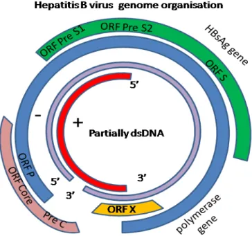
HBV infection data and history of chronic hepatitis disease were provided by the doctors in primary care centers according to earlier examinations and records. The serum HBV marker (anti-gens and antibodies of HBV) had been checked in most of recruited subjects before the study started. Most people now agree that screening for PLC in groups with HBV infection or with liver cirrhosis does detect PLC at an ear-ly stage [21]. Therefore, we plan use the HBV serum DNA as a cancer maker as HCC. The X gene of HBV seems to play an important role in HBV-associated he-patocarcinogenesis[22]. The human hepatitis B virus X gene encode a 17 KDa
pro-12
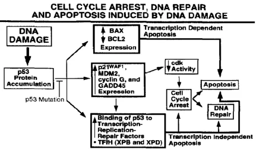
tein, named X, which is known to associated in insulin-like growth factor-II synthe-sized [6] (fig.1-7). In the physical pathway, insulin-like growth factor-II (IGF-II) is believed to function as a trigger for cell transformation, and malignant of hepatocyte tumor by autocrine or paracrine mechanisms (Fig. 1-8). X protein also complexes with the ~53 protein and inhibits its sequence specific DNA binding, transactivating and apoptotic capacity[22]. The p53 protein is a prototype tumor suppressor gene that is well suited for analysis of mutational spectrum in human cancer, it is the most common genetic lesion in human cancers, HBV X protein complexes with the p53 protein and inhibits its sequence specific DNA binding, transactivating and apoptot-ic capacity. (Fig. 1-9)
Fig. 1-7 Genome of human Hepatitis B Virus. Hepatitis B virus encode a 17 KDa
protein, named X, which is known to associated in insulin-like growth factor-II syn-thesized.
13
Fig 1-8 IGF-II physiology pathway. Insulin-like growth factor-II (IGF-II) is
be-lieved to function as a trigger for cell transformation, and malignant of hepatocyte tumor by autocrine or paracrine mechanisms. (Figure source: Nat Rev
Can-cer@2004 Nature Publishing Group)
14
the most common genetic lesion in human cancers, HBV X protein complexes with the p53 protein and inhibits its sequence specific DNA binding, transactivating and apoptotic capacity.
To summarize, HCC is one of the commonest malignancies in Asia. Clinical stu-dies have shown that only if HCC is detected at a presymptomatic stage can it be surgically resected with even the possibility of a cure. However, since HCC is usually associated with liver cirrhosis and there is often intrahepatic metastasis[21], surgical resection is suitable only for patients at an early stage of the disease. This means that early detection is the key of human to fight with HCC.
15
Chapter 2: Paper review
There are numerous important elements to alter the lift-time, stability, selectivity, and sensitivity of BioFET type sensor. The self-assemble monolayer functioned on the gate oxide is one of the most important element. The surface concentration, cloudy aggregation, duration, and crystalation of SAM will strongly influence the performance of sensor. Except the property of SAM, the concentration, temperature, pH, and ion contain also play a major role on capture ability, sensitivity, and selec-tivity of sensor. Fortunately, there are many research group have studied this region in the whole world, therefore, the paper which reported these subject is also abun-dant, following we will cite the literatures which we think are representative which we had reviewed (paper about SAN and buffer properties we will divided into two part). Naturally, and certainly the application of a BioFET is also important and in-terest for consider, so we also present some literature we have reviewed at the last part.
2.1 Literature about self-assembled monolayer
Aminated silane films are currently used in a wide variety of both industrial and research-oriented applications. Specifically, 3-aminopropyltriethoxysilane (APTES) is a commonly used coupling agent for the modification of silica surfaces to increase hydrophilic properties[1-4]. APTES is also used in attaching metal nanoparticles to silica substrates because of the strong interaction between the amine group and the metal particles[5][6]. APTES films are also used to promote protein adhesion for bi-ological implants and in lab-on-a-chip applications[13-15]. While many studies focus on the characterization of APTES[14-22], or other alkoxysilane films, most are li-mited in scope, focusing on single reaction variables or a narrow set of deposition
16
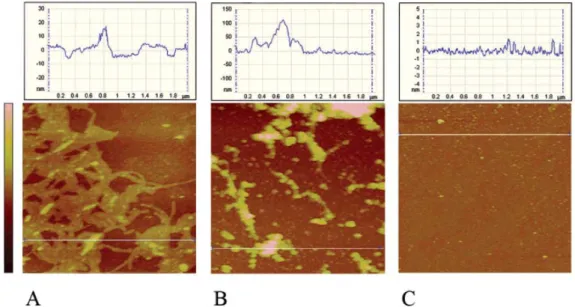
conditions without offering a clear, comprehensive guide to the best method of film formation. As a result, there is a wide range of reaction conditions used to deposit APTES films. Hydrolysis of silane drives the attachment of the APTES to the sub-strate resulting in siloxane bonds at the subsub-strate surface. Basic functional groups such as amines will self-catalyze the hydrolysis reaction leading to more aggressive monolayer formation as compared to nonaminated silanes[24]. The initial hydrolysis step can occur either in solution or at the substrate surface depending on the amount of water present in the system. An overabundance of water will result in excessive polymerization in the solvent phase, while a deficiency of water will result in the formation of an incomplete monolayer[25]. APTES films are subject to disorder, even as a monolayer, as it is possible for the amines to hydrogen bond to the substrate or for the entire molecule to bend such that the head-and-tail groups are oriented to-ward the substrate surface[24]. Solvent, concentration, reaction time, and reaction temperature also have an effect on the attachment kinetics. Incomplete coverage of the surface by APTES can be equally problematic. Understanding the mechanisms and kinetics of the monolayer formation is critical to creating well-controlled surfaces. The aim of this work is to establish the optimum reaction conditions for preparing uniform thin films of APTES on silica. The ideal film in this system will have maxi-mum surface coverage of amine functional groups and surface roughness on the order of the underlying substrate. AFM tapping mode scans are summarized as 3 X 3 grids in Fig.2-1. Each plane has nine separate surfaces all with the same reaction tempera-ture (75 °C on top and 25 °C on bottom). APTES concentration is presented along the x-axis, reaction time along the y-axis, and reaction temperature along the z-axis.
17
Fig. 2-1 APTES films scan by three-by-three matrix AFM. Each individual image
is 2 um X 2 um with a height scale of 200 nm (displayed left).
Fig. 2-2 Representative morphologies of APTES films. (A) Multilayer-island
18
(B) Rough APTES film deposited at 10%-24 h-75 °C, height scale is 150 nm. (C) Smooth APTES film deposited at 33%-24 h-75 °C, height scale is 10 nm. Horizontal lines indicate profile views.
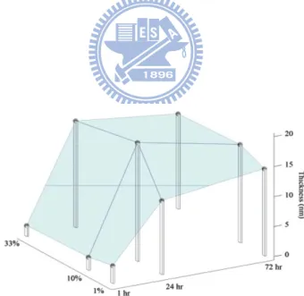
Increasing the concentration of the APTES solution for films deposited at 75 °C re-sulted in decreasing the RMS roughness for 24- and 72-h reactions (and it had a neg-ligible effect for 1-h reactions). For the 24-h reaction, this effect was realized only for the 33% solution, whereas the 72-h reaction resulted in an RMS decrease for both 10% and 33% solutions compared to 1% APTES solution. These three films depo-sited at 75 °C were smoother than their 25 °C counterparts. Ellipsometry was used to determine the thickness of the APTES films; the resulting data are presented graphi-cally in Figure 2-3.
Fig. 2-3 Ellipsometry data as a function of reaction. The experimental conditions
was 75 °C reaction temperature (left) and 25 °C reaction temperature (right).
When comparing samples at various APTES concentrations or temperatures when the APTES reaction is limited to 1 h, some important differences were apparent.
19
These interested phenomenons would be due to APTES hydrolysis can occur most efficiently and completely if there is sufficient surface water available for the reaction. The first monolayer of APTES reacts with a hydrated surface as shown in Figure 2-4 similar to the mechanism of deposition of trichlorosilanes[26][27]. As this reaction proceeds and a continuous film is formed, water is no longer concentrated at the film surface but is primarily in solution. As APTES concentration increases, it becomes more likely that water in the system will react with an unreacted APTES molecule as opposed to further hydrolyzing APTES molecules already deposited in the film. Thus, the APTES molecules deposited from a high APTES solution concentration are quickly buried before they can fully hydrolyze. As surface water is used up, the de-posited APTES can no longer attain high degrees of hydrolysis in the substrate sur-face.
Fig. 2-4 Chemical mechanism of APTES coating. APTES hydrolysis is followed
by condensation reaction in solution phase. Bottom scheme of APTES hydrolysis is followed by condensation at hydrated silica surface.
20
2.2 Literature about BioFET application
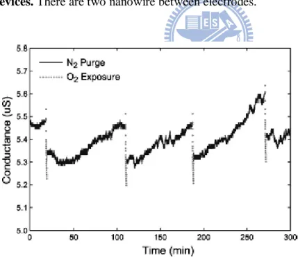
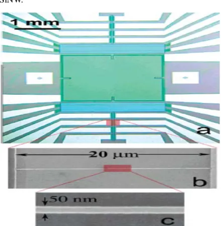
The detection of biological and chemical species is central to many areas of healthcare and the life sciences, ranging from uncovering and diagnosing disease to the discovery and screening of new drug molecules. Hence, the development of new devices that enable direct, sensitive, and rapid analysis of these species could impact humankind in significant ways. Devices based on nanobelts are emerging as a po-werful and general class of ultrasensitive, electrical sensors for the direct detection of biological and chemical species. [45] . Bashir and co-workers [28] described SiNW-FET sensor process that was realized using the top–down microelectronics processing techniques. A process known as confined was utilized to obtain single crystal silicon nano-plates that are thin as 7nm and nanobelts small as 40nm in di-ameter at precise locations, as shown in figure 2-5 [29]. The method allows the rea-lization of truly integrated dense array of sensor. Initial testing of the device showed that sensitivity towards oxygen ambient, and suggested it possibility of using these sensors for chemical and biological detection shown (figure 2-6) [28].
21
Fig. 2-5 Field emission scanning electron microscopy photos of the fabricated devices. There are two nanowire between electrodes.
Fig. 2-6 Gases responded by nanowire devices. Electrical current of the device is
responded to oxygen and nitrogen. Initial testing of the device showed that sensitiv-ity towards oxygen ambient.
22
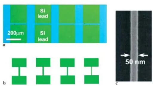
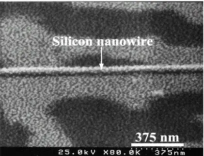
Li et al.[30, 31] fabricating a single crystal silicon nanobelt is with 50 nm and in width on SOI wafer by electron beam lithography. They have demonstrated the de-tection of DNA molecules based on their intrinsic charge by using SiNWs fabricated by top-down semiconductor processes. This method created a pathway for high-density, high-quality, and well organized nanoscale sensor that can be inte-grated with communication circuits, as shown in figure 2-7 [30]. Sequence-specific and label-free DNA sensors based on SiNW with probe-DNA or PNA molecules covalently immobilized on the surfaces (figure 2-8) [31]. Complementary DNA was recognized when the target DNA was complementary with the probe-DNA attached onto the SiNW surfaces, causes the change to accumulate on the surface of the SiNW.
Fig. 2-7 Optical and SEM image of nanowire sensor. (a) The optical image of the
central region of a sensor used for the DNA sensing study. (b) and (c) Representative SEM images showing the SiNW bridging two contact leads.
23
Fig. 2-8 Optical and SEM image of nanowire sensor. (a) Optical image of the
central region of a sensor showing a portion of the lead and the bridged nanowire used for the DNA sensing; (b) schematic drawing of the SiNW with varying widths corresponding to the image in (a); (c) a SEM image showing a 50-nm-wide SiNW, which extends between two contact leads.
Sheu et al. [32] demonstrated the bio-detection by using the SiNW whose sur-face was pretreated by APTMS and then selectively deposited with gold nanopar-ticles, as shown in figure 2-9 and figure 2-10 [32]. The GNPs on the surface served as linkers for detection. The target molecules bound with GNPs on the surface of the SiNB and resulted in a voltage shift.
24
Fig. 2-9 SEM image of SiNW after reaction of the GNPs with APTMS.
Fig. 2-10 ID-VG curves of SiNW after binding of different molecules on the
sur-face of SiNW. The turn-on voltage was changed after binding of different molecules
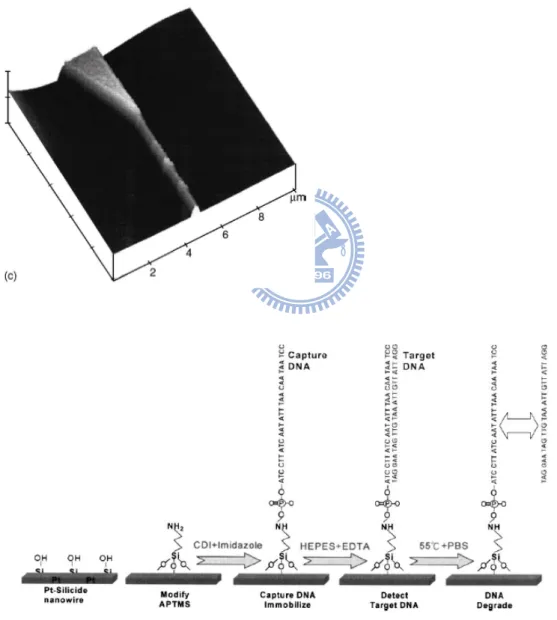
Ko et al. [33] developed a self-aligned platinum-silicide nanobelt (figure 2-11) for biomolecules sensing. The immobilization steps of the DNA onto the nanobelt are illustrated in figure 2-12. The 40 nm-width nanobelt is fabricated through a sequence of electron-beam writing on the poly-Si film, line shrinking by alkaline solution,
pla-25
tinum film depositing, 550 °C annealing, and aqua dissolution is performed. The im-mobilization of capture-DNA on the platinum-silicide nanobelt is verified from the fluorescence-labeled technique. The FET can distinguish the complementary, mis-matched, and dehybridized DNA via the conductance difference. They can sense the minimal target DNA concentration down to 100 fM.
Fig. 2-11 The 3-D AFM image of 40 nm width Pt-silicide nanowire, and the immobilization steps for the DNA on the Pt-silicide nanowire.
26
Eric Stern et al. [34] have demonstrated an approach to realize the characteristic of the SiNW sensors for specific antibody detection. The images and electrical proper-ties of the SiNW sensors are shown in figure 2-13. This approach has the pot ential for extending single device to an integrated system, with widely use as the chip-arrays. Successful solution-phase nanowire sensing has been demonstrated for ions [30, 31], proteins [32, 33], and DNA [34]. However, top-down fabrication of nanobelt devices [35, 36, 37] produced. Here they reported the uses of CMOS-FET compatible tech-nology and hence demonstrate the specific label-free detection of antibodies as well as real-time monitoring of the immune response.
Fig.2-12 Device fabrication and electrical performance. (a) Schematic of active
channel. The source, drain, and back-gate are labeled; (b) SEM and (c) OM image of a device; (d) ISD for varying VGD, illustrating p-type behaviour; (e) ISD for VGD
27
for forward and reverse sweep. (f) Hall and drift mobilities versus temperature.
Pritiraj Mohanty et al. [38] demonstrated the fabrication, functionalization, and operation of a nano-electronic FET for pH sensor, as shown in figure2-14. The SiNW with back-gate is fabricated with standard semiconductor process. The functionalized SiNW can be controlled with local back-gate to induce inversion or depletion layers. This approach offers the possibility of highly parallel detection of ion or charged protein and DNA with control of individual elements. By selective gating, individual NWs in an array can be turned on or off during sensing process. Therefore, the array contains multiple receptors for the detection of multiple chemical and biological spe-cies in a single integrated chip.
28
Fig. 2-13 Device schematic diagram. (a) The diagram of the SiNW with back-gate;
(b) The nanowire shown here; (c) A SiNW with a Au/Ti back-gate. (d) The SEM im-age displays three SiNW devices on the same chip; (e) An OM imim-age shows the flow chamber sealed on top of the devices.
2.3 Real-time Nanobelt Field-Effect-Transisitor Biosensors
Detectors based on semiconductor NWs are configured as FETs, which exhibit a conductivity change in response to variations in the electric field or potential at the surface [35]. The dependence of the conductance on gate voltage makes FETs natural candidates for electrically based sensing, because the electric field resulting from the binding of a charged species is the effect of applying a voltage with a gate electrode. They can be prepared as p- or n-type materials and configured as FETs in Figure
29
2-15(b) that exhibit electrical performance characteristics better achieved for planar silicon devices [39, 40, 41]. The superior switching characteristics of SiNWs are among the most important factors that affect sensitivity. The binding of biomolecules onto the surface of the NW leads to depletion or accumulation of carriers, versus only the surface region of a device. This semiconductor NWs provides sufficient sensitivi-ty to enable the detection of importing biomolecules in solution. However, because these are field-effect devices, detection sensitivity depends on the ionic strength of the solution. A sensing device can be configured from high-performance NW FETs by linking NW receptor groups that recognize specific molecules to the surface of the NW in figure 2-15(c). When the sensor device with surface receptors is exposed to a solution containing biomolecules, such as protein that has net negative charges in the aqueous solution, specific binding will lead to an increase in the surface and in con-ductance for a p-type NW device. As a proof of concept, they have developed a mi-crofluidic system integrated NW sensor that incorporates SiNWs with well-defined p- or n-type doping; source and drain electrodes that are insulated from the aqueous reagent environment, so that only processes occurring at the SiNW surface contribute to electrical signals; and a microfluidic channel for delivery of solutions in Figure 2-15(d) [42]. They fabricated electrically addressable arrays by a process that uses fluid-based assembly of NWs to align them and spacing over large areas [42]. Photo-lithography and metal deposition define interconnections to a large number of indi-vidual NWs in parallel in Figure 2-16.
30
Figure 2-14 NW-FET sensors. (a) Schematic of a p-type FET device. S, source; D,
drain; and G, gate electrodes; VG, gate voltage; (b) (left) TEM images of a 20-nm-diam single-crystal SiNW and (right) an OM image of a device; (c) Schematic of a sensor with antibody receptors (blue); binding of a protein with a net negative charge results in an increase in conductance; (d) NW sensor biochip with integrated microfluidic sample delivery.
31
Fig. 2-15 NW arrays for multiplexed protein sensing. (a) Illustration of NW array
fabrication; (b) Optical image of a NW array; (c) Data recorded from p-SiNW devices; NW1 was immobilized with PSA-Ab1, and NW2 was modified with ethanolamine; (d) Complementary sensing of PSA with p-type (NW1) and n-type (NW2) NW de-vices; (e) Schematic of array detection of multiple proteins; (f) Detection of PSA, CEA, and mucin-1 with NW1, NW2, and NW3 functionalized with antibodies. Pro-tein solutions of PSA, CEA, and mucin-1 were delivered sequentially to the array. (g) The drop of blood corresponds to the quantity required for analysis. Conductance versus time data recorded for the detection of PSA and PSA. NW2 was passivated
32
with ethanolamine.
Recently, the biosensor has employed increasingly in a variety of applications where continuous measurements in biological media are required by real-time moni-toring sensing. An electrochemical biosensor has been defined as a “self-contained integrated device, which is capable for providing specific quantitative or semi-quantitative information using a biological recognition element retained in di-rect spatial contact with an electrochemical transduction element” [42]. A biosensor is distinguished from a chemical sensor in that it possesses a biological recognition element, typically a protein, peptide or oligonucleotide. The goal in this subject may measure the rate of uptake or efflux of relevant species or to establish spatial distribu-tions in real-time sensing. [43]. When a sensor is brought in contact with biological tissues, sensor performance can deteriorate. The exact causes of this deterioration are not clear, but are a mix of passive adsorption of biomolecules on the sensor probe surface and active processes coupled to tissue response [43]. For this reason, we will give some attention to approve the microfluidic system that can play key roles in reg-ulation of detection events. This affords a greater range of analytical approaches to analysis, including separations and derivatization not possible with a single real-time sensor array.
33
Chapter 3: Experimental and material
3.0 Experimental process
The whole experimental procedure will divide into ten parts: (1) Fabrication of back-gated Silicon Nanobelt Field-Effect Transistor (NWFET), (2) self-assembly of APTES on the NWFET device for detection pH value of solution, (3) self-assembly of capture DNA on the NWFET device, (4) self-assembly of Antibody on the NWFET device, (5) fluorescence labeled capture DNA, (6) PDMS sample channel fabrication, (7) assemble the FET sensor to the whole system, (8) prepare the pH degree solution, (9) prepare the HBV gene, (10) Prepare the AFP sample in vitro or in vivo. These ten parts are not continuous process, and they will be discussed in more details in the following section.
3.1 Fabrication of back-gated silicon nanobelt field-effect
transistor (NB FET)
A back-gated nanobelt’s FET sensor was fabricated by using commercially avail-able 6-in. (100) silicon-on-insulator (SOI) wafers as the device substrate. The stacked films of TEOS-oxide and silicon nitride were deposited sequentially as the masking layer for local-oxidation of silicon (LOCOS) process. The underlying layer of TEOS-oxide, called a pad oxide, is used to cushion the transition of stresses be-tween the silicon and the nitride film. The active region and gate were then defined
by the optical lithography system (Canon FPA-3000i5 stepper). The composed
oxide/nitride stack layers were then plasma-etched, followed by the oxidation process was thermally grown. The patterned silicon nitride prevented the underlying silicon from oxidation and left the exposed silicon to be oxidized. As a result, the
34
active region including nanobelt, source, drain, and gate were defined due to the sil-icon nitride capped on top of the regions. In addition, the linewidth of nanobelts were shrunk due to oxidant diffused laterally during the oxidation process. This phenomenon, the “bird’s beak” effect, could induce the linewidth of nanobelts smaller than the critical width of the exposure system’s capability.
After the active region was patterned, As+ ion implant and rapid thermal anneal were carried out to form the source, drain, and gate region. Prior to defining the contact pad region by lithography and etching, the stacked Al-Si-Cu alloy onto tita-nium nitride metal film was formed by sputter system. Then, the silicon dioxide and silicon nitride layers were deposited to passivate the surface. The whole procedure was completed in National Chiao Tung University (NCTU) [1] or National Nano Device Laboratories (NDL) [2]. All of the medicine, reagents, and solvents were reagent-grade quality or higher level. The detection region of the back-gated NBFET was then etched back for the purpose of DNA immobilization. A schematic diagram of the fabricated back-gated NBFET biosensor is depicted in Fig. 3-1. The device after fabrication was stored in the clean room.
35
Fig. 3-1 Schematic Diagram of the NB FET fabrication process. Back-gated
na-nobelt’s FET sensor was fabricated by using 6-in. (100) silicon-on-insulator (SOI) wafers as substrate. The stacked films of TEOS-oxide and silicon nitride were depo-sited sequentially. Following coated the pad oxide. The active region and gate were then defined with the electron-beam writer. The composed oxide/nitride stack layers were then plasma-etched, followed by the oxidation process was thermally grown. After the active region was patterned, As+ ions implant and rapid thermal anneal were carried out to form the source, drain, and gate region. The sensing zone of the back-gated NBFET was then etched back for the purpose of DNA immobilization.
36
3.2 Self-assembly of APTES on the NBFET device for
solu-tion pH detecsolu-tion
Prior to immobilizing APTES, sensors were cleaned for 30 min using acetone and ethanol mixture for 1:1. High purity DI water, purified through double deioniza-tion processes, was used throughout. After cleaning process, a monolayer of APTES was then immobilized onto the NBFET surface (figure 3-2). The surface reactions occurred with the silanol groups present on the silicon NB surface as a result of na-tive oxide formation. Because silanol groups and APTES are good proton (H+) do-nors and acceptors, solution pH was hence detected by the variation of ions.
Fig. 3-2 Procedure of APTES immobilization on the NBFET surface. APTES
reactions with the silanol groups present on the silicon NW surface. Silanol groups and APTES on SiNB are applied for pH sensing.
37
3.3 Self-assembly of capture DNA on the NBFET device
After cleaning process described in section 3.2, a monolayer of 20-mer sin-gle-stranded DNA (named capture DNA, Blossom Biotechnologies, Taipei, Taiwan) molecules was then immobilized onto the NBFET surface. The surface reactions occurred with the silanol groups present on the silicon NB surface as a result of na-tive oxide formation. APTES and glutaraldehyde was employed as linker to self-assemble a monolayer of DNA onto the surface of NB detection region. Figure 3-3 illustrates the procedure for immobilization of the DNA molecules onto the sur-face-bounded APTES molecules. Initially, the samples were immersed into a 10% APTES aqueous solution for 30 min at 37 °C and adjusted to pH 3.5 with 1 M hy-drochloric acid. The samples were then rinsed with DI water and dried on a hot plate (120 °C for 30 min). At this stage, amino groups were presented as terminal units on the surface. Next, glutaraldehyde was linked to the amino groups to present alde-hyde groups on the surface; the sample was immersed in the linker solution [2.5% glutaraldehyde (1,5-pentanedial)] for 30 min at room temperature and then rinsed with phosphate-buffered saline (PBS, 120 mM NaCl, 2.7 mM KCl, and 10 mM phosphate buffer; pH 7.4; Sigma–Aldrich) solution (Yoshida et al., 1995). The 2.5% glutaraldehyde solution (Stefano et al., 2008; Yakovleva et al., 2002) was diluted with PBS solution from 25% glutaraldehyde (Sigma–Aldrich).Next, the selective immobilization technique was used to bind the terminal 3´-amino group of the oli-gonucleotide to the aldehyde groups on the NW surface. A fresh solution of synthet-ic 1 µM capture DNA (Blossom Biotechnologies, Taipei, Taiwan) was diluted with PBS buffer to provide a 10 nM solution of capture DNA. A portion (100 μL) of this capture DNA solution was dropped onto the NBs and reacted for 1 h to ensure effec-tive immobilization. The un-reacted aldehyde groups were blocked by ethanolamine
38
(Sigma–Aldrich), washed with PBS buffer, and subsequently dried under ambient nitrogen.
To ensure the immobilization efficiency of capture DNA, a fluorescence-labeled capture DNA (Blossom Biotechnologies, Taipei, Taiwan) was also prepared. The fluorescence used here was fluorescein isothiocyanate (FITC), which was specifi-cally modified in the 5’ end of the capture DNA. Green fluorescence images (excita-tion: 494 nm; emission: 520 nm) were observed using a BX51 fluorescence micro-scope (Olympus, PA, USA).
Fig. 3-3 Procedure of DNA Immobilization on the NBFET surface. APTES and
glutaraldehyde were employed as linker. In the next immobilization the terminal 3´-amino group modified DNA, this functional DNA is used as a capture molecular in order to binding the HBV X gene DNA fragment.
39
3.4 Self-assembly of antibody on the NBFET device
The AFP antibody was first diluted to 10 nM, and (Fitzgerald Industries Interna-tional, Inc. USA) was then modified on the NBFET surface. The surface reactions occurred with the silanol groups present on the silicon NB surface as a result of na-tive oxide formation. Figure 3-4 illustrates the procedure for immobilization of the protein molecules onto the surface-bounded APTES molecules. Initially, the samples were immersed into a 10% APTES anhydro solution for 30 min at 37 °C. The sam-ples were then rinsed with DI water and dried on a hot plate (120 °C for 30 min). At this stage, amino groups were presented as terminal units on the surface. Next, glu-taraldehyde was linked to the amino groups to present aldehyde groups on the sur-face; the sample was immersed in the linker solution [2.5% glutaraldehyde (1,5-pentanedial)] for 30 min at room temperature and then rinsed with phos-phate-buffered saline (PBS, 120 mM NaCl, 2.7 mM KCl, and 10 mM phosphate buffer; pH 7.4; Sigma–Aldrich) solution. The 2.5% glutaraldehyde solution was diluted with PBS solution from 25% glutaraldehyde (Sigma–Aldrich).Next, the se-lective immobilization technique was used to bind the amino group of the antibody onto the aldehyde groups on the NB surface. The un-reacted aldehyde groups were blocked by ethanolamine (Sigma–Aldrich), washed with PBS buffer, and subse-quently dried under ambient nitrogen.
40
Fig. 3-4 Procedure of antibody coated on SiNB. APTES and glutaraldehyde was
employed as linker for coated anti-AFP anti body for AFP sensing. The anti-AFP we used has a amino group in its constant region for reduce with aldehyde group of glutaraaldehyde.
3.5 Fluorescence labeled capture DNA
To ensure the immobilization efficiency of capture DNA, a fluorescence-labeled capture DNA (Blossom Biotechnologies, Taipei, Taiwan) was also prepared. The fluorescence used here was fluorescein isothiocyanate (FITC), which was specifi-cally modified in the 5’ end of the capture DNA. A fluorescence images (excitation: 494 nm; emission: 520 nm) were observed using a BX51 fluorescence microscope (Olympus, PA, USA), in order to ensure that the capture DNA exactly coated on the sensing zone of our BioFET type sensor.
41
Fig. 3-5 Procedure of FITC-DNA immobilized. APTES and glutaraldehyde was
employed as linker for FITC-DNA immobilized. A fluorescence images (excitation: 494 nm; emission: 520 nm) were observed using a BX51 fluorescence microscope.
3.6 PDMS sample channel fabrication
The fabrication of the microfluidic channel and integration with the NWFET is a necessary step for automatic sample delivery. We manufacture PDMS (sylgard 184A) to form structure, which contain a sample delivery channel. The PDMS is purchase from Sil-More Industrial Ltd.
The PDMS was mixed with the cure agent for 10:1, the mixture was then dropped to the 10 cm dish container. The 10 cm dish container was prior fixed with the 50 um in-diameter iron rod as the mold of channel. After pumping out the micro bubble and the froth inner PDMS, the PDMS was dried bake at 70℃ in an oven for four
42
hours. The next is the drawing of pattern, and cutting the PDMS to I-shape structure. The following figure is the process of I-shape channel and the cross section of the channel.
Fig 3-6 Schematic diagram of the microfludic channel fabrication process. (a)
10 cm dish. (b) Metal rods are immobilized on the 10 cm dish to create the chaneel mold. (c) Mixed the PDMS with the cure agent (10:1), and dropped the mixture to the 10 cm dish container. (d)Pumping out the micro bubble and the froth inner PDMS, the PDMS will dry bake in 70℃ for four hours. (e) Drawing of pattern of the microchannel.(f)Cutting the PDMS microchannel to I form structure. (g) Cross section of the channel.
3.7 Assemble the FET sensor to the system
We us ed the metal holder and acrylics gasket to clip the FET sensor and I-shape PDMS channel to prevent samples leakage. We used plastics tube for sample trans-fer and waste liquid exported. Finally, the syringe pump was employed as a motive
43
power to automatic sample transmission.
3.8 Preparation of the pH degree solution
In general, a health people has body fluid or blood that pH value is between 7.35-7.45, sometimes also called alkaline body chemistry. Therefore, the pH range for cells to survive in the internal environment is quite narrow. In general, PH under 7.35 may be considered acidosis, and PH over 7.45 may be considered alkalosis. Some more deviation, with PH under 7.30 or PH over 7.50, means more severe ac-id-base imbalance, which can be life-threatening. When a human is infected to cancer, the blood pH usually decreased, this is a good reason for us to utilize pH de-tection of blood to know the health situation of our body.
We dissolved the phosphate buffered saline pill (P4417-100TAB, purchase from SIGMA) into 200 ml DI water. The NaOH and HCl was used to modulate the pH of sample. We prepared pH value of 6.4-7.4 to test the FET sensor pH detection ability. The pH sample was simulated the healthy, sub-healthy, and disorder physiological fluid of our body.
3.9 Preparation of the HBV X gene DNA fragments
Recent study indicated that the HBV DNA will leakage to the plasma through its replication circle. All HBV x gene fragments we use as sample is synthesis by che-mistry procedure (purchase from MDBio[3-5], Inc.), the DNA sequence we applied is list in following table. All the DNA are dissolve in PBS buffer (pH 7.4), and stored in -20℃.
44
Sequence of the capture DNA 5'-NH2-ACGTCCCGCGCAGGA-3'
Sequence of target DNA 5'-TCCTGCGCGGGACGT-3'
Target DNA with 1 base mismatch 5'-TCCTGCGAGGGACGT-3'
Target DNA with 5 bases mismatch 5'-TCCTGACACTGACGT-3' Non-complimentary DNA 5'-GAACCACACTAGATG-3'
Tab le 3-1 Lists of the capture, target, one-base, five-base, and non-complementary DNA sequence. Sequence of the capture DNA is the fragment
of DNA that complementary to the HBV X gene, which we coated on the SiNB FET sensor; Sequence of target DNA is DNA fragment whice sequence is mimic the HBV X gen DNA sequence; Target DNA with 1 base mismatch is complementary to the
Sequence of the capture DNA but with one base mismatch in the medium; Target DNA with 5 bases mismatch is complementary to the Sequence of the capture DNA
but with five base mismatch in the medium; Non-complimentary DNA is a random sequence which cannot hybrid to Sequence of the capture DNA.
3.10 Preparation of the AFP sample in vitro or in vivo
AFP (AFP, α-fetoprotein) is a protein [6] [7] which in humans is encoded by the
afp gene [8][9] . AFP is produced by the yolk sac and the liver during fetal life.
Like any elevated tumor marker, elevated AFP by itself is not diagnostic, only sug-gestive. Tumor markers are used primarily to monitor the result of a treatment (e.g. chemotherapy). If levels of AFP go down after treatment, the tumor is not growing. In the case of babies, after treatment AFP should go down faster than it would nor-mally. A temporary increase in AFP immediately following chemotherapy may indi-cate not that the tumor is growing but rather that it is shrinking (and releasing AFP as the tumor cells die). AFP-L3, an isoform of AFP which binds Lens culinaris
ag-45
glutinin, can be particularly useful in early identification of aggressive tumors asso-ciated with hepatocellular carcinoma (HCC). AFP is the main tumor marker (some-times with HCG) used to monitor testicular cancer, ovarian cancer, and malignant teratoma in any location: values of AFP over time can have significant effect on the treatment plan. For this reason, AFP is a valuable detection target for our FET bio-sensor. All AFP is purchase from Blossom Biotechnologies Inc. Taipai, Taiwan, and the all are reagent-grade quality. All the AFP samples is store in the -20 ℃.
46
Chapter 4 Result and Discussions
4.1 Physical and electrical properties of the back-gate
SiNB-FET
The back-gated silicon nanobelt field effect transistors (NWFETs) on sili-con-on-insulator wafer were successfully fabricated. The width of nanobelt is about 60nm (figure 4-1 top). It is as same as the traditional metal oxide semiconductor (MOSFETs), the values of Id can be well controlled by the applied gate voltage (Fig. 4-1(b) (c). In this case, an n-channel FET is applied a gate voltage (Vg) from
nega-tive to posinega-tive direction to induce neganega-tive charge in the channel. When the gate voltage was smaller, p-n junction was blocked the electrical current from drain to source, and there was a very low leakage current (Ioff) in the level of picoampere
(pA). When the gate voltage is high enough, construct the conducting inversion layer and ‘open’ the channel, the drain-to-source current (Id) increase outstanding
and the gate voltage is called ‘threshold voltage (Vth). The threshold voltage of FET
was about -1.5 V. The current (Ion) reach different saturation dependant on different
applied drain-to-source voltage (Vd). The ON/OFF current ratio is about 5 orders of
magnitude. The Id-Vd curve also depends on controlled gate voltage (Vg), and
back-gate SiNB-FET biosensors were characterized the physical and electrical prop-erties by 4156C semiconductor analyzer.
47 (a) (b) Gate voltage (V) -4 -2 0 2 4 D rai n cu rren t ( A ) 10-12 10-11 10-10 10-9 10-8 10-7 10-6 10-5 Vd = 0.1 and 1 V Drain voltage (V) 0 1 2 3 4 5 D rai n cu rren t ( µA) 0 2 4 6 8 Vg = -2 to 5 V Step = 1 V
Fig. 4-1 (a) SEM image of silicon nanobelt. The width of nanobelt is about
60nm. (b) Electrical properties of SiNB FET sensor. The threshold voltage of FET we fabrication is about -1.5 V, The ON/OFF current ratio is about 5 orders. The Id-Vd curve dependant on controllable gate voltage (Vg), and the current (Ion)
reach different saturation dependant on different drain-to-source voltage (Vd) we