White p - i - n organic light-emitting devices with high power efficiency and stable color
Meng-Huan Ho, Shih-Feng Hsu, Jia-Wei Ma, Shiao-Wen Hwang, Pu-Cheng Yeh, and Chin H. Chen
Citation: Applied Physics Letters 91, 113518 (2007); doi: 10.1063/1.2784971 View online: http://dx.doi.org/10.1063/1.2784971
View Table of Contents: http://scitation.aip.org/content/aip/journal/apl/91/11?ver=pdfcov Published by the AIP Publishing
Articles you may be interested in
Chemical changes on the green emitter tris(8hydroxyquinolinato)aluminum during device aging of p i n -structured organic light emitting diodes
Appl. Phys. Lett. 95, 183309 (2009); 10.1063/1.3257380
High efficiency p - i - n top-emitting organic light-emitting diodes with a nearly Lambertian emission pattern J. Appl. Phys. 106, 063114 (2009); 10.1063/1.3225998
Very low voltage and stable p - i - n organic light-emitting diodes using a linear S,S-dioxide oligothiophene as emitting layer
Appl. Phys. Lett. 94, 063510 (2009); 10.1063/1.3072798
Extremely low voltage and high bright p - i - n fluorescent white organic light-emitting diodes Appl. Phys. Lett. 92, 113304 (2008); 10.1063/1.2898401
Highly efficient p - i - n -type organic light emitting diodes on ZnO:Al substrates Appl. Phys. Lett. 91, 063510 (2007); 10.1063/1.2768865
This article is copyrighted as indicated in the article. Reuse of AIP content is subject to the terms at: http://scitation.aip.org/termsconditions. Downloaded to IP: 140.113.38.11 On: Thu, 01 May 2014 00:07:54
White p-i-n organic light-emitting devices with high power efficiency
and stable color
Meng-Huan Hoa兲and Shih-Feng Hsu
Department of Applied Chemistry, National Chiao Tung University, Hsinshu, Taiwan 300, Republic of China
Jia-Wei Ma
Department of Photonics, National Chiao Tung University, Hsinshu, Taiwan, Republic of China and Institute of Electro-Optical Engineering, National Chiao Tung University, Hsinshu, Taiwan 300, Republic of China
Shiao-Wen Hwang, Pu-Cheng Yeh, and Chin H. Chen
Display Institute, Microelectronics and Information Systems Research Center, National Chiao Tung University, Hsinshu, Taiwan 300, Republic of China
共Received 25 June 2007; accepted 24 August 2007; published online 13 September 2007兲 Highly efficient p-i-n two-component white organic light-emitting devices have been fabricated with a thin dual emission layer system comprised of one codeposited emitting layer with blue and yellow dyes and one blue emitting layer, which gives rise to a balance white emission. The p-i-n white device achieved an electroluminescence efficiency of 10 cd/ A and a power efficiency of 9.3 lm/ W at 1000 cd/ m2 and a low voltage of 3.4 V with a Commission Internationale
de l’Eclairage coordinates of 共0.32, 0.43兲. The electroluminescent color of this p-i-n white organic light-emitting diode device has been shown to be immune to drive current density variations. © 2007 American Institute of Physics. 关DOI:10.1063/1.2784971兴
Organic light-emitting diodes共OLEDs兲 are of consider-able interest in recent years for flat panel display applica-tions, particularly in white OLEDs共WOLEDs兲 which have attracted a lot of commercialization interests due to their demonstrated applications in the fabrication of full color dis-plays with a color filter,1 or as backlight for liquid crystal displays as well as in solid-state lightings.2,3 WOLEDs coupled with color filter for full color displays can circum-vent the problematic issues of high resolution shadow mask and achieve higher effective aperture ratio of pixels. How-ever, with this approach, the color filters will invariably lower the brightness of the full color display. In order to obtain low power consumption as well as bright and sharp display image, the development of highly efficient and stable WOLEDs has become one of the major endeavors in the OLED community.4
White-light emission which requires the mixing of two complementary colors or three primary colors have been widely reported.5–7Careful control of the location of exciton recombination zone共RZ兲 and the energy transfer between the host and dopant molecules have been shown to be critical in obtaining a balanced white emission of high efficiency.8,9 WOLEDs based on phosphorescent emitter systems10,11have the highest reported efficiencies which can achieve up to 100% internal quantum efficiency. However, most of these highly efficient phosphorescent OLEDs decrease rapidly with increasing drive current, and the operating reliability still requires further research and improvement.10
By introducing p-i-n structure to an OLED device, the operating voltage can be considerably reduced for both fluorescent12and phosphorescent13systems. The highly con-ductive p- and n-doped layers could enhance the charge
in-jection from the contacts and reduce the Ohmic losses in these layers.12 To further reduce the drive voltage in p-i-n OLEDs, the thickness of low conductive layer based on or-ganic materials should be as thin as possible. However, it is difficult for WOLEDs with multiemission layer to achieve a stable white color due to the shift of RZ in thin organic layer, which often leads to undesirable CIEx,y color change with respect to drive current.
In this study, we demonstrate a dual emission layer 共DEML兲 system for p-i-n WOLEDs in which the first emis-sion layer is the codopant emitting layer with 2-methyl-9,10-di共2-naphthyl兲anthracene 共MADN兲:14
5% N , N
⬘
-bis共1-naphthyl兲-N,N
⬘
-diphenyl-1 , 1⬘
-biphenyl-4 , 4⬘
-diamine 共NPB兲:3% p-bis共p-N,N-diphenyl-aminostyryl兲benzene共DSA-Ph兲:14
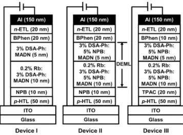
0.2% rubrene共Rb兲 and the second one is a blue emitting layer of MADN:5% NPB:3% DSA-Ph. Three types of p-i-n WOLED devices have been fabricated, as depicted in Fig.1. The total thickness of DEML in these p-i-n devices is only 15 nm. Device I is the p-i-n WOLED without code-posited NPB in the DEML system while device II is the
p-i-n WOLED with the DEML system. The pure NPB layer
of device II was replaced with 1,1-bis关N,N-di 共p-tolyl兲aminophenyl兴cyclohexane15 共TPAC兲 as electron
blocker in device III. In our p-i-n architecture, 50% v/v tung-sten oxide 共WO3兲 doped NPB and 2% cesium
carb-onate 共Cs2CO3兲 doped 4,7-diphenyl-1,10-phenanthroline
were used as the p-doped transport layer 共p-HTL兲 and
n-doped transport layer共n-ETL兲, respectively. In the DEML
system, MADN, NPB, DSA-Ph, and Rb were used as host material, assistant dopant, blue, and yellow fluorescent dop-ants, respectively. For comparison, we also fabricated a con-ventional WOLED device with structure of ITO/ CFx/ NPB
共50 nm兲/NPB:1.2% Rb 共20 nm兲/MADN:3% DSA-Ph 共40 nm兲/tris共8-quinolinolato兲aluminum 共Alq3兲 共10 nm兲/LiF
共1 nm兲/Al 共150 nm兲, in which CFx, NPB, and Alq3 were a兲Author to whom correspondence should be addressed; electronic mail:
APPLIED PHYSICS LETTERS 91, 113518共2007兲
0003-6951/2007/91共11兲/113518/3/$23.00 91, 113518-1 © 2007 American Institute of Physics
This article is copyrighted as indicated in the article. Reuse of AIP content is subject to the terms at: http://scitation.aip.org/termsconditions. Downloaded to IP: 140.113.38.11 On: Thu, 01 May 2014 00:07:54
used as the hole injection material,16hole, and electron trans-port materials, respectively.
It is known that Rb with lowest unoccupied molecular orbital/highest occupied molecular orbital of 3.2/ 5.4 eV can be a carrier trap for electrons, especially at low electric field,17 which will cause the problematic white emission color change with various drive currents in thin emission layer of p-i-n two-component WOLEDs. In order to alleviate the unstable color issue associated with the carrier-trapping property of Rb, we have purposely coevaporated Rb with low doping concentration of 0.2% and 3% DSA-Ph in MADN, which would cause the yellow emission generated by the energy-transfer process from blue to yellow emitter. The energy-transfer process can be demonstrated by the solid-state emission spectra depicted in the inset of Fig. 2, the thin film composed of MADN:3% DSA-Ph:0.2% Rb emits intense yellow emission and relatively weak blue-greenish emission. It is evident that the emission of MADN around 430 nm essentially quenched and there is an effective energy-transfer characteristic from DSA-Ph to Rb, which is primarily due to the favorable spectral overlap between the emission peak of DSA-Ph and the absorption peak of Rb at 495 nm.18
Therefore, we designed and developed a DEML system by inserting a blue emitting layer of MADN:3% DSA-Ph
after the coevaporated EML into the structure of device I to enhance the blue emission intensity. From the inset of Fig.2, the electroluminescence 共EL兲 spectrum of device I indeed shows the enhancement of the blue emission intensity with respect to the solid PL of coevaporated thin film. However, the yellow emission intensity is still much higher than the blue emission, leading to undesirable white emission with CIEx,ycoordinates of共0.37, 0.47兲. Furthermore, a significant
EL color shift of device I is observed with respect to various drive currents as the CIEx,y coordinates are shifted from
共0.410, 0.496兲 at 1 mA/cm2 to 共0.321, 0.419兲 at
100 mA/ cm2 with ⌬CIE
x,y= ±共0.089,0.077兲, as shown in
the inset of Fig. 3, in which the yellow emission intensity decreases with the increasing current density. We inferred the unstable EL color is due to the RZ shifts toward the blue emitting layer under high current stress.
Therefore, we codeposited 5% NPB in the DEML sys-tem of device II as the assistant dopant with the purpose of shifting the RZ toward the blue emitting layer to balance the blue and yellow emission intensities under low current den-sity. Figure 2 reveals that device II also has a better J-V characteristic than device I which indicates that NPB mol-ecules play an important role in enhancing the hole transport in the DEML system. In addition, the EL spectrum of device II depicted in the inset of Fig. 2 shows a more balanced white emission with CIEx,yof共0.33, 0.43兲 at 20 mA/cm2and
the relative intensity of blue light has been increased as com-pared with device I. This phenomenon which exhibits the codeposited NPB molecules can indeed shift the RZ to the blue emitting layer and improve white CIEx,y coordinates. Moreover, the EL color shift with respect to varying drive currents has also been improved to ⌬CIEx,y= ±共0.05,0.04兲
from 1 to 100 mA/ cm2, as shown in the inset of Fig. 3.
However, the reduced relative intensity of yellow emission leads to a lower EL efficiency of 7.4 cd/ A at 20 mA/ cm2.
To further enhance the efficiency and improve the color stability of these p-i-n white devices, we turn to refine the exciton confinement in device III, in which the NPB layer
FIG. 1. Schematic device architecture of p-i-n WOLEDs.
FIG. 2. Current density–voltage共J-V兲 characteristics of devices I and II. Inset: solid PL spectrum of composite thin film and EL spectra of devices I, II, and III at 20 mA/ cm2.
FIG. 3. Power efficiency vs luminance characteristics of devices II and III. Inset: CIEx,ycoordinates vs current density characteristics of devices I, II, and III.
113518-2 Ho et al. Appl. Phys. Lett. 91, 113518共2007兲
This article is copyrighted as indicated in the article. Reuse of AIP content is subject to the terms at: http://scitation.aip.org/termsconditions. Downloaded to IP: 140.113.38.11 On: Thu, 01 May 2014 00:07:54
was replaced by TPAC with a high LUMO energy level 共2.0 eV兲 and high hole mobility 共10−4– 10−3cm2/ V s兲,15
which can be an effective electron-blocking as well as hole transport material. Indeed, both blue and yellow intensities of device III have been enhanced, as shown in the inset of Fig. 2, and its emission achieved a white CIEx,y of 共0.32,
0.43兲. Furthermore, the EL performance can be boosted to 9.9 cd/ A and 8.2 lm/ W at 20 mA/ cm2. It is also observed that the white emissive color becomes more stable with re-spect to drive current density as the EL color shift is only of ⌬CIEx,y= ±共0.013,0.009兲 from 1 to 100 mA/cm2, as shown
in the inset of Fig.3.
Detailed EL performances of these devices measured at 20 mA/ cm2 are summarized in Table I. All p-i-n white de-vices show a much lower drive voltage and a dramatic gain in power efficiency as compared with those of conventional white device. Figure 3 shows the power efficiency versus luminance characteristics of devices II and III. Device III can achieve 10 cd/ A and 9.3 lm/ W at 1000 cd/ m2 which are
considerably better than those of device II with 7.3 cd/ A and 6.8 lm/ W. It is noteworthy that both L-V and J-V curves of device III are steeper than those of conventional white de-vice, as depicted in Fig. 4. The threshold voltage of device III is around 2.9 V. When driven at 6 V, device III can reach 10 000 cd/ m2 which is nearly eight times brighter than the
conventional device. These results prove that the efficient exciton confinement is one of the most important factors in controlling the RZ shift under various drive currents and it is also indispensable for the development of a highly efficient and color stable p-i-n WOLED.
In summary, we have demonstrated highly efficient p-i-n WOLEDs with a dual emission layer 共DEML兲 system. The codeposited NPB molecules in the DEML were used as the assistant dopant共NPB兲 to shift the RZ towards the blue emit-ting layer and balance the blue and yellow emission intensi-ties. In addition, the refined exciton confinement of p-i-n WOLEDs has been shown to significantly improve the EL performance, giving rise to 10 cd/ A and 9.3 lm/ W at 1000 cd/ m2 and a stable white color under various drive
conditions.
This work was supported by a grant from Chunghwa Picture Tubes, Ltd.共CPT兲 of Taoyuan, Taiwan. The authors also thank e-Ray Optoelectronics Technology Co., Ltd. of Taiwan for supplying some of the OLED materials studied in this work.
1J. Kido, K. Nagai, and K. Okutama, Appl. Phys. Lett. 64, 815共1994兲. 2P. Destruel, P. Jolinat, R. Clergereaux, and J. Farenc, J. Appl. Phys. 85,
397共1999兲.
3B. W. D’Andrade and S. R. Forrest, Adv. Mater.共Weinheim, Ger.兲 16, 1585共2004兲.
4A. Saitoh, N. Yamada, M. Yashima, K. Okinaka, A. Senoo, K. Ueno, D. Tanaka, and R. Yashiro, Proceedings of the Society For Information
Dis-play Boston, Massachusetts, 2005, p. 28.
5A. Dodabalapur, L. J. Rothberg, and T. M. Miller, Appl. Phys. Lett. 65, 2308共1994兲.
6R. S. Deshpande, V. Bulovic, and S. R. Forrest, Appl. Phys. Lett. 75, 888 共1999兲.
7T. H. Liu, Y. S. Wu, M. T. Lee, H. H. Chen, C. H. Liao, and C. H. Chen, Appl. Phys. Lett. 85, 4304共2004兲.
8C. H. Kim and J. Shinar, Appl. Phys. Lett. 80, 2201共2002兲.
9J. T. Lim, N. H. Lee, Y. J. Ahn, G. W. Kang, and C. H. Lee, Curr. Appl. Phys. 2, 295共2002兲.
10B. W. D’Andrade, R. J. Holmes, and S. R. Forrest, Adv. Mater. 共Wein-heim, Ger.兲 16, 624 共2004兲.
11S. Tokito, T. Iijima, T. Tsuzuki, and F. Sato, Appl. Phys. Lett. 83, 2459 共2003兲.
12J. Huang, M. Pfeiffer, A. Werner, J. Blochwitz, S. Liu, and K. Leo, Appl. Phys. Lett. 80, 139共2002兲.
13G. F. He, O. Schneider, D. S. Qin, X. Zhou, M. Pfeiffer, and K. Leo, J. Appl. Phys. 95, 5773共2004兲.
14M. T. Lee, H. H. Chen, C. H. Tsai, C. H. Liao, and C. H. Chen, Appl. Phys. Lett. 85, 3301共2004兲.
15P. M. Borsenberger, L. Pautmeier, R. Richert, and Bässler, J. Chem. Phys.
94, 8276共1991兲.
16L. S. Hung, L. R. Zheng, and M. G. Mason, Appl. Phys. Lett. 78, 673 共2001兲.
17B. Wei, K. Furukawa, M. Ichikawa, T. Koyama, and Y. Taniguchi, Mol. Cryst. Liq. Cryst. 426, 295共2005兲.
18Y. S. Wu, T. H. Liu, H. H. Chen, and C. H. Chen, Thin Solid Films 496, 626共2006兲.
FIG. 4. Luminance–current density–voltage共L-J-V兲 characteristics of con-ventional white device and device III.
TABLE I. EL performances of white devices driven at 20 mA/ cm2.
Device Voltage 共V兲 Yield 共cd/A兲 Efficiency 共lm/W兲 CIEx,y Conventional 6.4 9.0 4.4 共0.32, 0.41兲 I 4.4 9.1 7.1 共0.37, 0.47兲 II 3.6 7.4 6.4 共0.32, 0.43兲 III 3.8 9.0 8.2 共0.32, 0.43兲
113518-3 Ho et al. Appl. Phys. Lett. 91, 113518共2007兲
This article is copyrighted as indicated in the article. Reuse of AIP content is subject to the terms at: http://scitation.aip.org/termsconditions. Downloaded to IP: 140.113.38.11 On: Thu, 01 May 2014 00:07:54