INTRODUCTION
For the bonding of recycled sputtering targets to their backing plates, soldering has been commonly employed as a low-temperature joining method. Owing to environmental concerns for Sn-Pb solders and the avoidance of costly In-based solders, Sn-Zn alloys have been considered as one alternative be-cause they also possess the advantages of high strength, good creep resistance, and high thermal fatigue resistance.1By adding Bi into Sn-Zn solders, the melting point can be decreased, and the greater the amount of Bi rendered, the lower the melting point.2 Bismuth also helps improve the wettability and corrosion performance of Sn-Zn solders.3 How-ever, the formation of the Bi-rich phase in Bi-con-tained solders might weaken the mechanical proper-ties of the soldered joints.3
Although copper is widely used as the backing-plate material for sputtering targets, its high erosion into Sn-based solders has constituted an annoying problem. To eliminate this problem, a nickel backing plate or copper deposited with nickel as a diffusion barrier is considered. The interfacial reactions be-tween Sn-Zn-Bi solders and Ni substrates during the soldering process are thus worth investigating. For the thermal aging (solid/solid) reactions and solder-ing (liquid/liquid) reactions between pure Bi and Ni substrates, a number of researchers have reported
only on NiBi3 intermetallic compounds (IMCs) that form at the Bi/Ni interface.4–9The NiBi3 intermetal-lic compounds appear not only at the Bi/Ni interface but also in the Bi solder matrix due to the dissolu-tion of Ni into liquid Bi.7,9According to their investi-gations, the NiBi3formed as a layer at the interface, which the compound in the Bi solder matrix forms as large needles. During thermal aging of a Bi/Ni diffu-sion couple, the growth kinetics of NiBi3at the inter-face is diffusion-controlled.4,5 In the case of Sn-58Bi/Ni interfacial reactions, a Ni3Sn4IMC has been observed.9–11Kinetics analyses have been conducted for thermally aged specimens, and the growth of such Ni3Sn4 IMCs has been shown to be diffusion-controlled with an activation energy of 90 kJ/mol.10 The interfacial reactions of Sn-8.5Zn-5.5Bi solders with nickel, copper, brass, and nickel-iron substrates after thermal aging at a temperature of 125°C for 100 days have also been studied, and the appearance of Ni5Zn21 IMCs was reported.3 When Sn-8.5Zn-5.5Bi solders react with Ni and other substrates, the growth kinetics of interfacial IMCs has not been in-vestigated. Therefore, this study identifies the IMCs formed during the soldering reactions between liq-uid Sn-8Zn-3Bi solders and Ni substrates at temper-atures ranging from 225°C to 400°C. In addition, the growth kinetics of these IMCs is evaluated.
EXPERIMENTAL
The Sn-8Zn-3Bi (wt.%) solder was prepared by en-capsulating pure Sn (99.9%), Zn (99.9%), and Bi
Intermetallic Compounds Formed during Interfacial Reactions
between Liquid Sn-8Zn-3Bi Solders and Ni Substrates
M.Y. CHIU, S.S. WANG, and T.H. CHUANG
Department of Materials Science and Engineering, National Taiwan University, Taipei 106, Taiwan The morphology and growth kinetics of intermetallic compounds (IMCs) formed at the interfaces between liquid Sn-8Zn-3Bi solders and nickel sub-strates in the temperature range from 225°C to 400°C are investigated for the applications in bonding recycled sputtering targets to their backing plates. The results show that a continuous single layer of Ni5Zn21IMC appears at temper-atures below 325°C, while a double layer containing Ni5Zn21and Ni35Zn22Sn43 IMCs is formed at temperatures above 325°C. In both cases, the growth kinet-ics of IMCs is interface-controlled. During the growth of IMCs, their reaction fronts migrate in the direction of the solder much more rapidly than toward the nickel substrate, and erosion of the Ni substrate is quite slight.
Key words: Sn-8Zn-3Bi solder, nickel substrate, intermetallic compound,
linear growth kinetics
(Received August 10, 2001; accepted January 16, 2002)
Intermetallic Compounds Formed during Interfacial Reactions
between Liquid Sn-8Zn-3Bi Solders and Ni Substitutes 495
(99.99%) in a quartz tube at a vacuum level of 10⫺5 torr and melting at 600°C. The melting point of this solder was analyzed by a differential scanning calorimeter (DSC). The heating rate of the DSC is 10°C/min under N2atmosphere.
For the solder reactions, the Sn-8Zn-3Bi solder ingot was cold-rolled into 0.2-mm-thick foil. Then, the solder foils were sliced into specimens (10 mm⫻ 8 mm⫻ 0.1 mm). A 1-mm-thick Ni plate (99.9% Ni) was cut into the same size as the solder foils. The Ni substrates were ground with SiC paper, polished with 1 and 0.3m Al2O3 powder, cleaned with ace-tone and alcohol, and dipped with rosin mildly acti-vated (RMA) type flux. The Sn-8Zn-3Bi solder foil was placed on the Ni substrate and the sample was heated in an infrared furnace under a vacuum of 10⫺3torr. Soldering was performed in the tempera-ture range between 225°C and 400°C; for 10 to 150 min, then, the sample was rapidly cooled to the room temperature in 2 min.
The soldered specimens were cut along the cross section, ground with SiC paper, polished with 1 and 0.3 m Al2O3 powders, and ultrasonically cleaned with acetone and alcohol. The microstructure of the interface was investigated with a scanning electron microscope (SEM). The composition of the IMCs was identified by an electron-probe microanalyzer (EPMA) and x-ray diffractometer (XRD). The sam-ples for XRD analyses were prepared by selectively etching out the unreacted solder with a solution consisting of 1 mL HF, 15 mL H2SO4, and 84 mL H2O. In order to clarify the formation mechanism of the IMC, the surface of Ni substrate was par-tially sputter-coated with a Ta thin film. Because the Ta thin film does not react with the solder or the substrate, it could well serve as a reaction marker to identify the original interface between Ni(s)and solder(l).
RESULTS AND DISCUSSION
The DSC analyses of the Sn-8Zn-3Bi solder reveal a sharp endothermic peak at 197.7°C, which is near the melting point (198.5°C) of the eutectic binary Sn-9Zn alloy. Figure 1 illustrates the microstructure
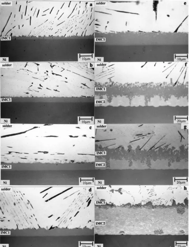
of the as-cast Sn-8Zn-3Bi solder, which possesses a great deal of platelike Zn-rich precipitates (shown in black), as well as a small amount of Bi-rich precipi-tates (white) embedded in the -Sn matrix (gray). The morphology of IMCs formed at the Sn-8Zn-3Bi/Ni interfaces after soldering reaction at various temperatures for 120 min is shown in Fig. 2. There is only one type of IMC that appears at the interface at lower temperatures (below 325°C). The EPMA re-sults from Table I give the composition profile of such an IMC: 17.07 to 18.29 Ni, 79.22 to 80.75 Zn, 0.17 to 2.24 Sn, and 0 to 0.05 Bi (at.%). The composi-tion corresponds to a stoichiometric Ni5Zn21type of IMC, which can be confirmed by the XRD analyses of the reacted specimen after selectively etching the solder. For most based solders such as Pb, Sn-Bi, Sn-Ag, and Sn-Cu, their interfacial reactions with Ni substrates result in the formation of Ni3Sn4 IMC. The appearance of a different IMC (Ni5Zn21) at the Sn-8Zn-3Bi/Ni interface is attributed to the ac-tive nature of the element Zn. In Fig. 2, when the soldering temperatures increase to above 325°C, a double layer of IMCs can be observed. Table I shows that the outer layer (IMC1) possesses a composition similar to that of the IMC formed at temperatures below 325°C when the Sn and Bi contents are slightly higher. In contrast, the composition of the inner intermetallic layer (IMC2) is 29.93 to 34.78 Ni, 21.12 to 22.70 Zn, 43.00 to 48.70 Sn, and 0.09 to
Fig. 1. Morphology of the as-cast Sn-8Zn-3Bi solder.
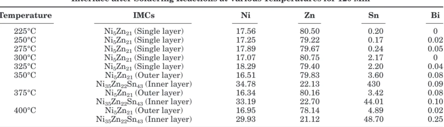
Table I. Chemical Compositions (At.%) of the IMCs Formed at the Sn-8Zn-3Bi/Ni Interface after Soldering Reactions at Various Temperatures for 120 Min
Temperature IMCs Ni Zn Sn Bi 225°C Ni5Zn21(Single layer) 17.56 80.50 0.20 0 250°C Ni5Zn21(Single layer) 17.25 79.22 0.17 0.02 275°C Ni5Zn21(Single layer) 17.89 79.67 0.24 0.05 300°C Ni5Zn21(Single layer) 17.07 80.75 2.17 0 325°C Ni5Zn21(Single layer) 18.29 79.40 2.20 0.04 350°C Ni5Zn21(Outer layer) 16.51 79.83 3.60 0.08 Ni35Zn22Sn43(Inner layer) 34.78 22.13 430 0.09 375°C Ni5Zn21(Outer layer) 16.34 80.16 3.42 0.08 Ni35Zn22Sn43(Inner layer) 33.19 22.70 44.01 0.10 400°C Ni5Zn21(Outer layer) 16.95 78.14 4.89 0.02 Ni35Zn22Sn43(Inner layer) 29.93 21.12 48.70 0.25
Fig. 2. The SEM micrographs of the intermetallic compounds formed at Sn-8Zn-3Bi/Ni interface after soldering reactions at various tempera-tures for 120 min: (a) 225°C, (b) 250°C, (c) 275°C, (d) 300°C, (e) 325°C, (f) 350°C, (g) 375°C, and (h) 400°C.
Fig. 4. Growth of single layer of intermetallic compound during the soldering reactions between Sn-8Zn-3Bi and Ni substrate at 250°C for various times: (a) 60 min, (b) 90 min, (c) 120 min, and (d) 150 min.
termetallic layer (IMC1) to grow with the increase of reaction time. It is obvious that at 400°C the growth of Ni35Zn22Sn43 (IMC2) becomes predomi-nate. The total thickness (x) of the double layer
(IMC1 ⫹ IMC2) formed at temperatures above
325°C is also plotted on the same log x vs. log t Intermetallic Compounds Formed during Interfacial Reactions
between Liquid Sn-8Zn-3Bi Solders and Ni Substitutes 497
0.25 Bi (at.%). Such a composition corresponds to a stoichiometric Ni35Zn22Sn43type of IMC.
Though partial sputtering of the Ta thin film on the surface of the Ni substrate sets up a reaction barrier between 8Zn-3Bi and Ni, the original Sn-8Zn-3Bi/Ni interface can be marked. From Fig. 3, a slightly sunken curvature is formed at the Sn-8Zn-3Bi/Ni interface in the area adjacent to the Ta marker, which only implies that a small amount of Ni dissolved from the Ni substrate into the liquid Sn-8Zn-3Bi solder. For the soldering reactions at higher temperatures (e.g., 375°C), the Ta marking pinpoints the original Sn-8Zn-3Bi solder interface to be situated between the IMC1/IMC2 interface and the IMC2/Ni reaction front. In all cases, the reaction fronts of the IMCs migrate much more rapidly in the direction of the Sn-8Zn-3Bi solder.
The Ni5Zn21 type IMC formed at temperatures below 325°C grows with an increase of reaction time, as shown in Fig. 4. The thickness (x) of such inter-metallic layers formed at temperatures below 325°C is measured and plotted on a log x vs. log t scale, as shown in Fig. 5. The slopes of these plots give the n values of the kinetic relation x ⫽ tn. The n values range from 0.92 to 1.24, which implies that the growth of such Ni5Zn21 intermetallic layers is interface-controlled.
For the soldering reactions between Sn-8Zn-3Bi and Ni substrate above 325°C, SEM micrographs in Figs. 6 and 7 show that the Ni35Zn22Sn43 inter-metallic layer (IMC2) forms after the Ni5Zn21
in-Fig. 3. Growth of intermetallic compounds (IMCs) at Sn-8Zn-3Bi/Ni interface after soldering reaction at (a) 300°C and (b) 375°C for 120 min. (The original interface was marked with a Ta thin film.)
Fig. 5. The thickness (x) of Ni5Zn21intermetallic layers formed after
soldering reactions between Sn-8Zn-3Bi and Ni substrate at various temperatures below 325°C as a function of time (t).
Fig. 6. Growth of double layer of intermetallic compounds (IMC1: Ni5Zn21, and IMC2: Ni35Zn22Sn43) during the soldering reactions
be-tween Sn-8Zn-3Bi and Ni substrate at 350°C for various times: (a) 15 min, (b) 30 min, (c) 60 min, and (d) 120 min.
scale, as shown in Fig. 8. The n values ranging from 0.72 to 1.10 suggest a linear relationship. The results indicate that the growth of double-layer IMCs during the soldering reactions between Sn-8Zn-3Bi and Ni above 325°C is also interface-controlled.
For most soldering reactions, the growth kinetics of IMCs formed at the interfaces between liquid sol-ders and solid substrates has been shown to be dif-fusion-controlled.5,12–15An interface-controlled reac-tion was reported by Tu and Thompson for the growth of Cu6Sn5 IMCs at the interface between thin Cu and Sn films.16In that case, the release of Cu atoms from the Cu film into Sn was considered as the rate-limiting step in such a linear growth. In this present study, the linear growth of IMCs during the soldering reactions between liquid Sn-8Zn-3Bi and Ni substrates could be attributed to the rapid diffusion of Zn atoms in the solder matrix and IMCs, which constitutes the rate-limiting step for the reac-tion between Zn and Ni at the interface.
CONCLUSIONS
During the soldering reactions between liquid Sn-8Zn-3Bi and Ni substrates at temperatures ranging from 225°C to 325°C, a continuous single layer of Ni5Zn21 IMC appears at the Sn-8Zn-3Bi/Ni inter-face. However, in a higher temperature range from 325°C to 400°C, a double layer containing Ni5Zn21 and Ni35Zn22Sn43IMCs can be observed. In all cases, plots of the thickness of IMCs as a function of reac-tion time show a linear reacreac-tion, which indicates that the growth kinetics of these IMCs is interface-controlled. Through the marking of the original Sn-8Zn-3Bi/Ni interface using a Ta thin film, it is evi-dent that the Ni substrate dissolves only slightly into the liquid Sn-8Zn-3Bi solder, and the reaction
front of the IMC on the side of the Sn-8Zn-3Bi solder migrates much more rapidly than its counterpart on the other side.
Intermetallic Compounds Formed during Interfacial Reactions
between Liquid Sn-8Zn-3Bi Solders and Ni Substitutes 499
REFERENCES 1. N.C. Lee, Adv. Microelectron. 26, 29 (1999).
2. Yoshikazu Nakamura, Yoshinori Sakakibara, Yoshihisa Watanabe, and Yoshiki Amamoto, Soldering Surface
Mount Technol. 10/1, 10 (1998).
3. Paul Harris, Soldering Surface Mount Technol. 11/3, 46 (1999).
4. O.V. Duchenko and V.I. Dybkov, J. Mater. Sci. Lett. 14, 1725 (1995).
5. V.I. Dybkov and O.V. Duchenko, J. Alloy Compounds 234, 295 (1996).
6. C.R. Kao, J. Mater. Sci. Eng. A 238, 196 (1997).
7. M.S. Lee, C. Chen, and C.R. Kao, Chem. Mater. 11, 292 (1999).
8. M.S. Lee, C.M. Liu, and C.R. Kao, J. Electron. Mater. 28, 57 (1999).
9. S.K. Kang, R.S. Rai, and S. Purushothaman, J. Electron.
Mater. 25, 1113 (1996).
10. C. Chen, C.E. Ho, A.H. Lin, G.L. Luo, and C.R. Kao, J.
Elec-tron. Mater. 29, 1200 (2000).
11. B.L. Young and J.G. Duh, J. Electron. Mater. 30, 878 (2001).
12. D.R. Flanders, E.G. Jacobes, and R.F. Pinizzotto, J.
Elec-tron. Mater. 26, 883 (1997).
13. L.H. Su, Y.W. Yen, C.C. Lin, and S.W. Chen, Metall. Mater.
Trans. B 28B, 927 (1997).
14. S.K. Kang and V. Ramachandran, Scripta Metall. 14, 421 (1980).
15. S. Choi, Y.R. Bieler, J.P. Lucas, and K.N. Subramanian, J.
Electron. Mater. 28, 1209 (1999).
16. K.N. Tu and R.D. Thompson, Acta Metall. 30, 947 (1982).
Fig. 7. Growth of double layer of intermetallic compounds (IMC1: Ni5Zn21, and IMC2: Ni35Zn22Sn43) during the soldering reactions
be-tween Sn-8Zn-3Bi and Ni substrate at 400°C for various times: (a) 15 min, (b) 30 min, (c) 60 min, and (d) 120 min.
Fig. 8. The total thickness (x) of double layer (Ni5Zn21 ⫹
Ni35Zn22Sn43) intermetallic layers formed after soldering reactions
between Sn-8Zn-3Bi and Ni substrate at various temperatures above 325°C as a function of time (t).