Effect of bias stress on mechanically strained low temperature polycrystalline
silicon thin film transistor on stainless steel substrate
I-Hsuan Peng, Po-Tsun Liu, and Tai-Bor Wu
Citation: Applied Physics Letters 95, 041909 (2009); doi: 10.1063/1.3193654
View online: http://dx.doi.org/10.1063/1.3193654
View Table of Contents: http://scitation.aip.org/content/aip/journal/apl/95/4?ver=pdfcov Published by the AIP Publishing
Articles you may be interested in
Anomalous on-current and subthreshold swing improvement in low-temperature polycrystalline-silicon thin-film transistors under Gate bias stress
Appl. Phys. Lett. 98, 122101 (2011); 10.1063/1.3568895
Electrical characteristics and mechanical limitation of polycrystalline silicon thin film transistor on steel foil under strain
J. Appl. Phys. 106, 114502 (2009); 10.1063/1.3264839
Effect of mechanical strain on mobility of polycrystalline silicon thin-film transistors fabricated on stainless steel foil
Appl. Phys. Lett. 91, 243507 (2007); 10.1063/1.2824812
Stress-induced width-dependent degradation of low-temperature polycrystalline silicon thin-film transistor Appl. Phys. Lett. 90, 183502 (2007); 10.1063/1.2734504
Characteristics and stress-induced degradation of laser-activated low temperature polycrystalline silicon thin-film transistors
J. Appl. Phys. 93, 1926 (2003); 10.1063/1.1535732
This article is copyrighted as indicated in the article. Reuse of AIP content is subject to the terms at: http://scitation.aip.org/termsconditions. Downloaded to IP: 140.113.38.11 On: Wed, 30 Apr 2014 14:58:40
Effect of bias stress on mechanically strained low temperature
polycrystalline silicon thin film transistor on stainless steel substrate
I-Hsuan Peng,1,a兲 Po-Tsun Liu,2,b兲 and Tai-Bor Wu1
1Department of Materials Science and Engineering, National Tsing-Hua University, 101, Section 2,
Kuang-Fu Road, Hsinchu, Taiwan 30013, Republic of China
2Department of Photonics and Display Institute, National Chiao Tung University, 1001 Ta-Hsueh Rd.,
Hsinchu, Taiwan 300, Republic of China
共Received 6 February 2009; accepted 10 July 2009; published online 31 July 2009兲
This paper reported the variation in performance of bias stressed low-temperature polycrystalline silicon thin film transistors 共LTPS TFTs兲 fabricated on metal foil substrate for flexible display applications. The mobility, threshold voltage共Vth兲, and trap density 共Nt兲 of the proposed p-channel
poly-Si TFT as a function of curvature radii were investigated. The significant increase in Vthby 9% was observed as the compressive or tensile mechanical strain increases to 0.1%. In addition, the hole mobility increases by 7% due to an increased compressive strain of 0.1%, while hole mobility decreases by 3.5% with the increase in tensile strain of 0.1%. After dc bias stressing, the LTPS TFT with mechanical strain had better performance than that on flat state in both the mobility drop and
Vthshift. Mechanical strain influences the lattice arrangement and electric field at the drain electrode region that resisted device degradation in early stressing period. © 2009 American Institute of
Physics. 关DOI:10.1063/1.3193654兴
Among many foldable substrate candidates, steel foil substrate is very attractive due to its thin, lightweight, flex-ible, and rugged characteristics.1As compared with plastic substrates, the steel foil substrate is compatible with the tra-ditional manufacture process of thin film transistors 共TFTs兲 due to its higher melting point and better blocking against water vapor and oxygen permeability. In addition, the polycrystalline-Si 共poly-Si兲 TFTs has attracted much atten-tion because of the higher field-effect mobility than any other kinds of TFTs.2Previous researchers have reported the effect of tensile strain on the mobility of poly-Si TFTs.3 However, no further investigation was reported for the influence of bias stress on the mechanically strained poly-Si TFT devices. In this work, therefore, we study the effect of bias stress on the variations in threshold voltage, mobility, and trap density for the p-channel poly-Si TFT under uniaxial compressive and tensile strain induced by substrate mechanically bending.
The poly-Si TFT devices were fabricated on a stainless steel foil with Young’s modulus 200 GPa 共thickness = 70 m, area= 10⫻10 cm2兲 by conventional low-temperature polycrystalline silicon共LTPS兲 process. Because the roughness of bare steel foil was not suitable for TFT process, it was mechanically polished first. A 2 m thick spin-on-glass共SOG兲 buffer layer was coated on the polished steel foil in order to obtain a smoother surface with surface roughness共Ra兲 of about 0.499 nm compared to polished
sur-face 0.89 nm. The SOG was formed by spin coating and baked in an oven under 450 ° C for 2 h. A 0.3 m thick SiO2 buffer layer and a 50 nm thick amorphous hydrogenated sili-con共a-Si:H兲 layer were deposited sequentially at a plasma-enhanced chemical vapor deposition 共PECVD兲 system. Fol-lowing the dehydrogenation, the a-Si film was crystallized
by typical XeCl excimer laser annealing共ELA兲 with a wave-length of 308 nm and an energy density of 400 mJ/cm2. After ELA process, poly-Si channel layer was patterned and a 100 nm thick silicon dioxide as gate dielectric was depos-ited by PECVD. A self-aligned boron doping technology was used to form p+ source and drain regions with a dose of 2⫻1015 ions/cm2 at 70 keV. Thermal annealing was con-ducted at 450 ° C by rapid thermal process to activate the dopant in the source and drain regions. After the deposition of a 300 nm thick PECVD interlayer dielectric SiNxfor
pas-sivation layer, a metallization consisting of a 200 nm thick chromium共Cr兲 was applied for the source/drain metal elec-trode. The compressive strain or tensile strain was applied to the poly-Si TFTs on metal foil parallel to the source-drain current path. The characteristic of TFT devices was mea-sured as a function of strain under mechanical bending in-ward or outin-ward. Both channel width共W兲 and channel length 共L兲 of the poly-Si TFT device are 20 m. Under dc stress condition, we applied drain and gate bias voltage of⫺20 V, with stressing times 0, 1000, and 2000 s under flat, compres-sive 共Rn= 10兲 and tensile 共Rp= 10 mm兲 status.
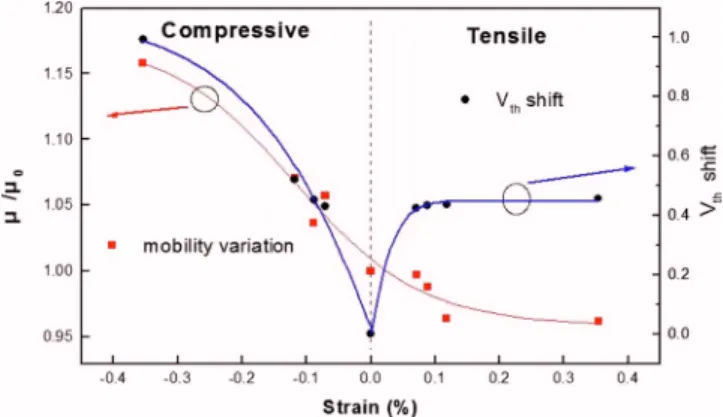
The p-channel LTPS TFT has exhibited superior field-effect mobility of 92 cm2/V s, a threshold voltage of ⫺5.7 V, and an on/off current ratio higher than 107and sub-sthreshold slope of 0.85 V/decade without mechanical stress. Figure1shows the variation in field-effect mobility 共兲 and
Vthof poly-Si TFTs on metal foil under tensile and compres-sive strains with curvature radius共R兲. The strain on the sur-face is calculated by4 surface=
冉
df+ ds 2R冊
共1 + 2+ x2兲 共1 +兲共1 + x兲, 共1兲 where = df/ds and x = Yf/Ys, where df= 2.8 andds= 70 m are film and substrate thickness, respectively.
Young’s modulus of film and substrate for both Yfand Ysare
200 GPa.5The Vthincreased as the mechanical strength en-larged. The breakage of weak Si–Si bonds during mechanical
a兲Tel.: 886-3- 5715131 ext. 33893. FAX: 886-3- 5722366. Electronic mail:
b兲Author to whom correspondence should be addressed. Tel.: 886-3-5712121
ext. 52994. FAX: 886-3-5735601. Electronic mail: [email protected].
APPLIED PHYSICS LETTERS 95, 041909共2009兲
0003-6951/2009/95共4兲/041909/3/$25.00 95, 041909-1 © 2009 American Institute of Physics
This article is copyrighted as indicated in the article. Reuse of AIP content is subject to the terms at: http://scitation.aip.org/termsconditions. Downloaded to IP: 140.113.38.11 On: Wed, 30 Apr 2014 14:58:40
strain lead to creation of the dangling bonds and defect traps. The bond strength can be affected by the mechanical strain and thus the creation of dangling bonds depends on the sub-strate curvature.6
The variations in trap density of poly-Si film were ex-tracted to investigate the strain influence on the poly-Si TFT device. From Seto’s theory, it can be modeled the relation-ship between grain boundary potential barrier VBand doping
concentration ND共cm−3兲. When doping concentration ND
in-creased more than Nt/L, the grain boundary potential barrier
height VB can be expressed as the following equation:
VB= qn 2s
冉
Nt 2n冊
2 = qNt 2 8sn ,where Nt共cm−2兲 is the density of acceptorlike traps at grain
boundary, VB is the grain boundary potential barrier height,
and n 共cm−3兲 is the carrier concentration. As proposed by Levinson et al.7 and a better approximation for channel thickness tchin an undoped material,8the I-V characteristics including the trap density can be obtained by the following equation: ID=0Cox W L共VG− VFB兲VDexp
冉
− q2Nt2冑
ox/s Cox2 共VG− VFB兲2冊
.The effective trap state density then can be obtained from the slope of the curve ln关ID/共VG− VFB兲兴 versus 共VG− VFB兲−2. We calculated the trap density variation rate under different bending condition as shown in Fig. 2共a兲. Both tensile and compressive strain increased the trap density. The curve of trap density variation shows strong correlation with Vthshift but not with variation in Fig. 1. It was known that the carrier mobility is strongly correlated with trap density and reversely proportional to the trap density in the poly-Si film.9 The known theory generally serves the poly-Si TFT device without mechanical strain and the variation in carrier effec-tive mass. In this work, however, experimental results indi-cate that the trap density would not solely dominate the car-rier mobility of the strained poly-Si TFT devices. The integral effects originated from lattice torsion, carrier effec-tive mass, and trap density should be considered for the me-chanically strained TFT, which can be totally reflected in the parameter of activation energy共Ea兲. The values of Eafor the
poly-Si TFT under different strain states was extracted by the
varied temperature measurement ranging from 25 to 120 ° C, as shown in Fig.2共b兲.10The energy barrier height under the compressive stress is the lowest than those on the states of the flat and the tensile. A reduced Ea can contribute the
en-hanced hole mobility to the p-channel poly-Si TFT. There-fore, the compressive strain on poly-Si TFT results in the highest mobility among any other strain types discussed in Fig.1.
According to the study of p-channel metal oxide semi-conductor共PMOS兲 devices, biaxial tensile strains could im-prove PMOS and n-channel metal oxide semiconductor drain current simultaneously but uniaxial strain effects improve one device and depraving the other instead.11Three factors affect single crystalline silicon mobility: silicon thickness, surface orientation, and strain. In poly-TFT devices, the ef-fects of uniaxial tensile and compressive strain split the en-ergy band of light hole and heavy hole, and then reduce scattering effect, indicating the increase in mean free time.12,13 In addition, the mechanical strain makes apparent band warping, reducing the hole effective mass. Mobility is proportional to electric charge, mean free time, and reversed to electric/hole effective mass, and resultantly the uniaxial compressive could increase mobility.14
In PMOS devices, the highest hole mobility was in the 共110兲 direction parallel the source/drain current path because of carrier repopulation.12When the bending direction paral-leled to the surface orientation 共110兲, the tensile condition got low carrier mobility, whereas compressive condition get higher carrier mobility. Though poly-Si contains other
sur-FIG. 3. XRD analysis of polycrystalline Si film on steel metal foil. FIG. 1.共Color online兲 The field-effect hole mobility variation and threshold
voltage shift共⌬Vth兲 as a function of strain with bending radius R=⬁, ⫾50,
⫾40, ⫾30, and ⫾10 mm, respectively, at VD= −10 V.0is the initial hole
mobility of poly-Si TFT on flat substrate, whileis the one after mechani-cal strain.
FIG. 2. 共Color online兲 共a兲 The trap density variation rate under bending radius R =⬁, ⫾50, ⫾40, ⫾30, and ⫾10 mm, respectively. 共b兲 The extracted activation energy Eafor the poly-Si TFT under different bending conditions.
041909-2 Peng, Liu, and Wu Appl. Phys. Lett. 95, 041909共2009兲
This article is copyrighted as indicated in the article. Reuse of AIP content is subject to the terms at: http://scitation.aip.org/termsconditions. Downloaded to IP: 140.113.38.11 On: Wed, 30 Apr 2014 14:58:40
face orientations of grain, the 共110兲 surface acts as major effect when strain is performed. In Fig.3, the grain orienta-tion of poly-Si film on metal foil was analyzed by using x-ray diffractometer共XRD兲. The orientation of 共111兲, 共110兲, and 共100兲 is indicated in our samples. The signal pulses of 共400兲, 共220兲, and 共222兲 are the same to orientation 共100兲, 共110兲, and 共111兲, respectively. The obvious signal intensity of 共110兲 indicated higher drain current could be obtained while the poly-Si TFT device under compressive stress state.
Effects of bias stress on the mechanically strained poly-Si TFT device also were investigated in this work. In Fig.4共a兲, the compressive strain leads to less mobility drop than the flat and the tensile strain under initial stressing pe-riod 共⬍1000 s兲. The effect of compressive strain lightened carrier共i.e., hole兲 effective mass resultantly increased carrier mobility. The mobility enhancement originated from com-pressive strain partially compensated for an influence of dc stress on the mobility degradation. Figure4共b兲illustrates the applied strain effect along Si surface orientations共110兲. The strain effect on mobility shows good resistance to the degra-dation after bias stress. Higher carrier mobility under com-pressive strain makes TFT devices more stable in dc bias stress condition.
In summary, the LTPS TFTs were fabricated on steel foil. Threshold voltage shift and trap density variation were
observed under compressive and tensile strains. The holes mobility was enhanced by compressive strain while degraded by tensile strain. In addition, the carrier mobility and on-state current are decreased obviously after dc bias stress with me-chanical strain applied. Meme-chanical strain influences the lat-tice distance and electric field at the drain region, which resist device degradation in early stressing period. The pro-posed poly-Si TFT maintained good electrical characteristics, even when subjected to compressive or tensile mechanical strain with a bending radius of 10 mm under bias stress condition.
The authors would like to acknowledge the financial support of the National Science Council共NSC兲 under Con-tract Nos. NSC 96-2221-E-009-130-MY3, NSC 97-2218-E-009-003, and 97-2918-I-97-2218-E-009-003, and partially supported by MOEA Technology Development for Academia Project No. 95-EC-17-A-07-S1-046 and MOE ATU Program No. 95W803.
1E. Y. Ma and S. Wagner,Appl. Phys. Lett. 74, 2661共1999兲.
2M. Wu, X. Z. Bo, J. C. Sturm, and S. Wagner, IEEE Trans. Electron Devices 49, 1993共2002兲.
3P. C. Kuo, J. R. Abbas, and M. Hatalis, Appl. Phys. Lett. 91, 243507
共2007兲.
4S. W. Won, J. K. Cheng, C. B. Lee, and J. Jang,J. Electrochem. Soc. 151,
G167共2004兲.
5F. Templier, B. Aventurier, P. Demars, J. L. Botrel, and P. Martin,Thin Solid Films 515, 7428共2007兲.
6H. Gleskova, S. Wagner, W. Soboyejo, and Z. Suo, J. Appl. Phys. 92,
6224共2002兲.
7J. Levinson, F. R. Shepherd, P. J. Scanlon, W. D. Westwood, G. Este, and
M. Rider,J. Appl. Phys., 53, 1193共1982兲.
8P. Migliorato, C. Reita, G. Tallarida, M. Quinn, and G. Fortunato, Solid-State Electron. 38, 2075共1995兲.
9T. Serikawa, S. Shirai, K. Nakagawa, S. Takaoka, K. Oto, K. Murase, and
S. Ishida,Jpn. J. Appl. Phys., Part 1 35, 937共1996兲.
10M. C. Wang, T. C. Chang, P. T. Liu, S. W. Tsao, Y. P. Lin, and J. R. Chen, Electrochem. Solid-State Lett. 10, J113共2007兲.
11Y. J. Yang, W. S. Ho, C. F. Huang, S. T. Chang, and C. W. Liu,Appl. Phys. Lett. 91, 102103共2007兲.
12H. Irie,Tech. Dig. - Int. Electron Devices Meet. 2004, 225共2004兲. 13Z. Ren, P. M. Solomon, M. Yang, and K. Rim, J. Appl. Phys. 94, 1079
共2004兲.
14E. Ungersboeck, S. Dhar, G. Karlowatz, V. Sverdlov, H. Kosina, and S.
Selberherr,IEEE Trans. Electron Devices 54, 2183共2007兲.
FIG. 4.共Color online兲 共a兲 The mobility variation and threshold voltage shift in p-channel LTPS TFT devices under different mechanical strain as func-tion of dc stress time under gate and drain voltage of⫺20 V and 共b兲 the applied compressive strain effect along Si surface orientations共110兲.
041909-3 Peng, Liu, and Wu Appl. Phys. Lett. 95, 041909共2009兲
This article is copyrighted as indicated in the article. Reuse of AIP content is subject to the terms at: http://scitation.aip.org/termsconditions. Downloaded to IP: 140.113.38.11 On: Wed, 30 Apr 2014 14:58:40