Effects of Channel Width and Nitride Passivation
Layer on Electrical Characteristics of
Polysilicon Thin-Film Transistors
Chia-Chun Liao, Min-Chen Lin, Tsung-Yu Chiang, and Tien-Sheng Chao
Abstract—SiN passivation layers were found to yield better per-formance, suppress the kink effect, and improve the gate leakage current and gate-induced drain leakage (GIDL) of polysilicon thin-film transistors (TFTs). The SiN passivation layers deposited under different deposition conditions possess different character-istics due to their varying passivation effect. A physical mechanism is proposed to explain the double-hump phenomenon induced by incomplete trap passivation. Based on the analysis of width depen-dence, the better performance of the samples with SiN passivation layers was attributed not only to radical passivation of the defect states but also to radical passivation of preexisting defects in the gate oxide. Furthermore, using SiN passivation layers improves immunity to positive gate bias stress, negative gate bias stress, and hot-carrier stressing. Moreover, the manufacturing processes are simple (without the long processing time plasma treatment requires) and compatible with TFT processes.
Index Terms—Gate-induced drain leakage (GIDL), grain boundary, intragrain, kink effect, radical.
I. INTRODUCTION
R
ECENTLY, polycrystalline silicon (poly-Si) thin-film transistors (TFTs) have attracted much attention due to their application in active-matrix liquid crystal displays. Fur-thermore, there has been increasing interest in developing techniques for optimizing poly-Si TFTs because such devices are promising for high vertical density components in appli-cations where the high mobility of single-crystal MOSFETs is not mandatory. The transfer characteristics of poly-Si TFTs strongly depend on defects in the intragrain, grain boundary, and the gate dielectric. The deep states, which originate from the dangling bonds in grain boundaries, influence the thresh-old voltage and the subthreshthresh-old swing, whereas tail states, which originate from the intragrain defects, affect the field-effect mobility and the minimum leakage current [1], [2]. In order to achieve superior characteristics for poly-Si TFTs, many techniques to optimize the device performance by reducingManuscript received February 15, 2011; revised July 23, 2011; accepted August 6, 2011. Date of publication September 26, 2011; date of current version October 21, 2011. This work was supported by the National Science Council, Taiwan, under Contract NSC 97-2221-E-009-152-MY3. The review of this paper was arranged by Editor H. Shang.
The authors are with the Department of Electrophysics, National Chiao Tung University, Hsinchu 300, Taiwan (e-mail: [email protected]).
Color versions of one or more of the figures in this paper are available online at http://ieeexplore.ieee.org.
Digital Object Identifier 10.1109/TED.2011.2165214
the trap density or increasing the grain size of polysilicon have been proposed [3]. Therefore, passivation of these defects may improve the threshold voltage, subthreshold swing, and mobility characteristics.
Hydrogen passivation by hydrogen plasma treatment has been proposed as an effective way to improve TFT perfor-mance. However, poly-Si TFTs with hydrogen plasma treat-ment suffer a severe hot-carrier issue due to weak Si–H bonds. Therefore, NH3, F, and N2have been proposed to improve the immunity of the hot carrier by creating strong bonds, which are more difficult to break than Si–H bonds during hot-carrier stressing [4]–[8]. Nevertheless, the additional time necessary for plasma treatment is an important issue to overcome.
Silicon nitride film is one of the most promising materials for coating and passivation films used in electronic devices and mechanical parts [9]. It has been reported that SiN layers can improve the performance of bulk-silicon MOSFETs [10], fully depleted silicon-on-insulator MOSFETs [11], and amorphous Si (a-Si) TFTs [12]. Furthermore, using a silicon nitride pas-sivation layer is effective for suppression of theI–V kink in heterojunction field-effect transistors since the radicals can pas-sivate defects, leading to a reduction in the trapping/detrapping process [13]. It has been reported that using a plasma-deposited SiN layer as a high-concentration diffusion source of atomic hy-drogen is a promising approach for improving the performance of poly-Si TFTs [14]. However, few complete investigations of poly-Si TFTs with SiN passivation layers have been reported.
On the other hand, an appropriate choice of molecular frac-tion of nitrogen mixed with hydrogen is known to be effective in further enhancing the improvement in the plasma discharge [15]. However, the effect of the flow rate of different reactant gases on the deposition of the SiN layer for passivation of poly-Si TFTs has yet to be systematically investigated. In studying the impact of SiN deposition conditions on single-crystal MOSFETs, Lu et al. proposed that reducing the flow rate of the diluent gas as nitrogen results in better improvement in the interface state due to passivation by hydrogen radicals [16]. In this paper, we find that the deposition conditions of the SiN passivation layers affect the characteristics of the poly-Si TFT.
Plasma passivation requires a very long hydrogenation time (> 4 h) to passivate the strain-bond-related tail state [2]. To en-able fabrication of useful transistors without additional process-ing time, this paper investigates the effects of SiN passivation layers on the electrical characteristics of TFTs. The deposition
inside the gate dielectric. As a result, TFTs with SiN passivation layers not only exhibit improved initial TFT performance but also enhanced immunity to positive gate bias stress (PGBS), negative gate bias stress (NGBS), and hot-carrier stressing.
II. EXPERIMENTS
The poly-Si TFTs studied in this paper were prepared as follows: an a-Si film of 500 Å was deposited at 500 ◦C by low-pressure chemical vapor deposition (CVD) on thermally oxidized wafers. The wafers were annealed at 600 ◦C for 24 h to transform the amorphous film into Si, and the poly-Si films were patterned into active islands. After removal of the surface oxide, 30-nm-thick tetraethyl orthosilicate (TEOS) ox-ide was deposited at 680◦C. A 2000-Å-thick poly-Si layer was deposited and patterned as the gate electrode, which also serves as the mask for self-aligned implantation. The source/drain and gate regions were then implanted by phosphorous (15 keV at 5× 1015cm−2) and activated at 600◦C for 24-h annealing in a N2ambient. The SiN layers were deposited under four differ-ent deposition conditions by plasma-enhanced CVD (PECVD) with the same thickness of 3000 Å. The control sample was skipped in this step. Power, pressure, and temperature were set at 100 W, 137 Pa, and 300 ◦C, respectively. Table I shows the reactant and diluent gas flow rates used to investigate the effect of the nitride passivation layer. The samples were labeled N2-low, N2-med, N2-high, and SiH4-high. A 2000-Å PECVD oxide was then deposited at 300◦C in 2.5 min for all TFTs capped with a nitride passivation layer. For comparison, a PECVD oxide (5000 Å) passivation layer was deposited at 300 ◦C in 6.3 min on the control sample. Hence, all samples have passivation layers of identical thickness. After patterning of the contact holes, aluminum was deposited by physical vapor deposition and patterned as the probe pads to complete the TFT devices. For comparison, some devices underwent post-SiN-deposition thermal annealing in nitrogen at 350◦C for 60 min.
III. RESULTS ANDDISCUSSION A. Performance
Fig. 1 shows the ID–VG curves of n-channel TFTs for the control sample and the samples with the SiN passivation layer. The channel length and width are both 10µm. It is evident that n-channel TFTs exhibit improved performance with the capped SiN layer, as compared to control samples. The threshold
Fig. 1. Transfer characteristics (ID–VG) of n-channel TFTs with different passivation layers.
Fig. 2. Transconductance of n-channel TFTs with different passivation layers.
voltage and subthreshold swing are improved compared to the control sample, meaning that using SiN passivation appears to effectively terminate the dangling bonds in the poly-Si and SiO2/poly-Si interface. Furthermore, the gate-induced drain leakage (GIDL) is suppressed for the poly-Si TFTs with SiN capping compared to the control sample, which is attributed to trap passivation. The N2-high sample possesses the highest sub-threshold swing, whereas the SiH4-high sample possesses the lowest peak transconductance, as shown in Fig. 2. In contrast, the control sample possesses no peak transconductance due to the hole trapping. The N2-med and N2-low samples possess better transfer characteristics.
The aforementioned results indicate that the deposition con-ditions of SiN passivation layers affect the characteristics of poly-Si TFTs. Both the NH3 and N2 plasma passivation processes effectively improve TFT transfer characteristics by plasma discharge. However, NH3plasma treatment is more ef-fective than N2plasma treatment because the hydrogen radicals are most effective for passivating the grain boundary and trap states [6]–[8]. In this paper, during the deposition of SiN, the hydrogen and nitrogen radicals diffuse and passivate intragrain and grain-boundary trap state in poly-Si by forming Si–H and Si–N bonds. The reactant gas of NH3can generate the hydrogen
Fig. 3. Output characteristics (theID–VD curve) of n-channel TFTs with different passivation layers.
and nitrogen radicals, and the reactant gas of N2 plasma can generate only the nitrogen radicals. As a result, the deposition condition of SiN has a significant influence on the generation of radicals and on poly-Si TFT device performance.
Fig. 3 shows the drain-current-versus-drain-voltage (ID–VD) characteristics of all n-channel poly-Si TFTs. There are three distinct features of these characteristics. At low overdrive volt-age, all samples capped with SiN exhibit better performance than the control sample due to passivation of the tail state. As the overdrive voltage is further increased, however, the control sample has better performance than the SiH4-high sample due to hole trapping at higher gate voltage (discussed later). At higher drain biases, the “kink” effect is much more pronounced for the control sample than its counterparts. We believe that trap passivation is responsible for the suppressed kink effect. There are several models for the explanation of pronounced kink effect by trap. Kim et al. demonstrated that the kink effect de-pends on the nature of surface states [17]. Hack and Lewis pro-posed that the presence of grain boundaries or traps in poly-Si TFTs significantly enhanced the kink effects in poly-Si TFTs, as compared to single-crystal counterparts [18]. Kumar et al. predicted that the local electric field near the irregular surface due to grain boundaries can be appreciably greater than the average electric field, which can initiate additional impact ionization [19]. Thus, the reduced trap induced by the radicals is a reasonable explanation for the suppression of the kink effect. A high-quality gate oxide and interface between the gate oxide and the poly-Si channel are critical for transfer char-acteristics. Due to the nature of TEOS oxide, there are more dangling bonds and weak Si–O and Si–Si bonds in the bulk oxide and in the interface between the gate oxide and the poly-Si channel. Fig. 4 shows the gate leakage characteristics for all samples. The TFTs capped with SiN layers possess lower leakage than the control sample, indicating that using SiN passivation layers is an effective way to improve gate oxide quality. It has been reported that large amounts of nitrogen exist in oxynitride films. This enables formation of strong Si≡ N bonds in the oxynitride/poly-Si interface, which can improve gate leakage and charge trapping [20], [21]. Furthermore, NH3
Fig. 4. Gate leakage current of n-channel TFTs for all samples.
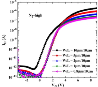
Fig. 5. Transfer characteristics (ID–VG) for the N2-high sample with differ-ent channel widths.
and H2 plasma treatments are effective in improving gate leakage [22]. Thus, passivation of defects in the bulk oxide, nitrogen pileup at the oxide/poly-Si interface, and improved interface state condition by nitrogen radicals are responsible for improving gate leakage during SiN deposition. As a result, using SiN passivation layers enables termination of both traps in the poly-Si channel and preexisting traps in the gate oxide by radicals.
B. Width Dependence of TFT Capped Nitride Passivation The transfer characteristics of the N2-high sample exhibit a double hump, as shown in Fig. 1, implying that hydrogen and nitrogen radical propagation is less effective. In order to clarify the double-hump phenomenon of the N2-high sample, we compared the transfer characteristics of the N2-high samples of different channel widths, as shown in Fig. 5. The double hump in the subthreshold region indicates the secondary con-duction path for the device with a width of 10µm. As the width is scaled down, the double-hump phenomenon is suppressed.
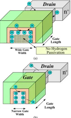
Fig. 6. (a) Cross section of n-channel TFTs with wider channel widths. Incomplete trap passivation is also indicated and is responsible for the double-hump phenomenon. (b) Cross section of n-channel TFTs with narrower chan-nel widths. Complete trap passivation appears to suppress the double-hump phenomenon.
A physical mechanism is proposed to explain the early turn-on phenomenturn-on for the device with a width of 10 µm. It is noted that the number of defects and available radicals affects the efficiency of passivating defects [1]. Trap passivation is not complete for the entire poly-Si channel for devices with a wider channel width, as shown in Fig. 6(a). A portion of the poly-Si channel, which was passivated by nitrogen or hydrogen radi-cals, has a lower local threshold voltage than the unpassivated portions of the channel, resulting in a nonuniform threshold voltage. Moreover, the nonuniform threshold voltage exhibits the early turn-on phenomenon. As the channel width is scaled down, the portion of the poly-Si channel without passivation by radicals is minimized, as shown in Fig. 6(b), and the double-hump phenomenon is suppressed since the radicals can diffuse and passivate the trap effectively.
In order to clarify the width effect on the devices’ electrical characteristics, a detailed investigation of the parameters of the poly-Si TFTs is necessary. Again, the threshold voltage, subthreshold swing, and maximum mobility strongly depend on the grain, grain boundaries, and interface properties. As shown in Fig. 7(a), TFTs capped with SiN passivation layers possess better subthreshold swing than the control sample for all dimensions, and the N2-low and SiH4-high samples have the lowest subthreshold swing. All samples with SiN passivation layers possess saturated features. These results indicate that passivation of the deep state in the grain boundary is efficient; hence, the decrease in the subthreshold swing is less dependent on the variation in channel width. Fig. 7(b) demonstrates the threshold voltage as a function of width. Threshold voltageVth
that not only increased passivation of the deep state but also increased passivation of preexisting defects in the gate oxide are the mechanisms by which the threshold voltage improves as the width is scaled down. It has been reported that the dominant pathway for hydrogen diffusion into the active poly-Si film may be through the gate oxide, where the diffusivity of hydrogen is much higher than in the poly-Si layer [1], [24]. Thus, passivation of the preexisting traps by hydrogen or nitrogen radicals is reasonable. As the channel width is scaled down, the portion of the poly-Si channel without passivation by radicals is minimized, resulting in more radical pileups at the oxide/poly-Si interface. Passivation of preexisting traps in the gate oxide becomes more efficient as channel width narrows, which is responsible for the improvement in the threshold voltage. The increase in mobility, along with the channel width decrease, is observed in Fig. 7(c). Two mechanisms may explain mobility’s dependence on the channel width. The first mechanism is the improvement in the interface state condition and enhanced passivation of the tail state in the poly-Si channel film at narrow channel widths. The second possible cause is the lower impact of the grain boundaries. At wider channel width, the SiH4-high sample has the lowest mobility, meaning that the SiH4-high sample has the lowest tail state passivation among all samples. The mobility for all TFTs capped with the SiN passivation layer becomes comparable at narrow channel widths. We believe that passivation of the tail state by the SiN passivation layer increases as the width falls, becoming similar for all nitride conditions at narrow channel widths, because the defects can be effectively passivated when a sufficient number of radicals is supplied.
In general, the improvements in threshold voltage and mobil-ity by nitride passivation become more significant as channel width is scaled down, because hydrogen or nitrogen radicals can terminate the strain bonds and more efficiently passivate the preexisting defects in the bulk oxide and interface. Moreover, the H2 plasma easily passivates dangling bonds in the grain boundaries to reduce the midgap deep states, whereas a very long hydrogenation time (> 4 h) is required to passivate the strain-bond-related tail state [2]. This theory is consistent with the effect of using a SiN passivation layer. In this paper, using a SiN passivation layer passivates the deep states and the strain-related tail state. Passivation of the deep states is rapidly sat-urated since the improvement in the subthreshold swing stays almost constant for all channel widths. On the other hand, the difference in mobility decreases for TFTs with different SiN passivation layers as the width is scaled down, meaning that
Fig. 7. (a) Variation of subthreshold swing as a function of channel width forL = 10 μm with different passivation layers. (b) Variation of threshold voltage as a function of channel width forL = 10 μm with different passivation layers. (c) Variation of field mobility as a function of channel width for L = 10 μm with different passivation layers.
Fig. 8. Threshold voltage shift as a function of stress time for n-channel TFTs under PGBS asVGS= 11 V.
passivation of the tail state is slow compared to passivation of the deep state.
C. PGBS, NGBS, and Hot-Carrier Stressing
Another important issue in poly-Si TFTs is reliability. The PGBS, NGBS, and hot-carrier stressing often degrade the re-liability of TFT devices. PGBS was carried out atVDS = 0 V andVGS = 11 V for 3000 s to examine the device reliability, as shown in Fig. 8. Tunneling of hot holes from the gate into the substrate may be responsible for positive charge trapping in the control sample during the initial stressing period, and electron trapping would then become the dominant trapping mechanism [25]. By contrast, samples capped with SiN passivation layers have smaller shift in threshold voltage than the control sample. NGBS was carried out atVDS= 0 V and VGS= −10 V for 1000 s to examine the device reliability, as shown in Fig. 9. The control sample exhibits significant electron trapping, whereas TFTs capped with SiN passivation layers show improved elec-tron trapping. These results show that using SiN passivation layers can improve the immunity of PGBS and NGBS.
Fig. 10(a) shows the dependence of dc hot-carrier degra-dation at a drain voltage VD of 18 V on overdrive voltage (VG− Vth) for all samples, where Ion is a drain current ID
Fig. 9. Threshold voltage shift as a function of stress time for n-channel TFTs under NGBS asVGS= −10 V.
at VG of 9 V and VD= 0.1 V, Ion0 is the initial value of Ion, and ΔIon is the decrease in Ion after 1000 s of stress. For bulk silicon, the worst dc hot-carrier degradation occurs when stress condition VG is about half of VD. However, the worst case stress condition of the TFT is lower than that of the bulk silicon. Toyota et al. found that the worst stress condition isVGS= 2 V at VDS = 10 V [26]. In this paper, we
found the lowest degradation at VGS− Vth= 5 V. Thus, we believe that the significant degradation of drain current below VGS− Vth= 5 V is attributable to hot-carrier-induced damage, and the degradation of drain current above VGS− Vth = 5 V is attributable to PGBS-induced damage. In contrast, samples capped with SiN passivation layers show slight variation in the drain current (below 5%). The threshold voltage shift and the relative variation of transconductance of TFTs with and without SiN passivation layers are shown in Fig. 10(b) and (c), re-spectively. Samples capped with SiN passivation layers exhibit improved threshold voltage shift and mobility degradation. The improved immunity of hot-carrier stressing for samples with SiN passivation layers is comparable to that for samples with plasma treatment in the literature [27], [28].
We found that TFTs capped with SiN passivation layers show improved immunity to PGBS, NGBS, and hot-carrier stressing. We believe that this improvement is due to passivation of
Fig. 10. (a) Dependence ofIondegradation under dc stress on gate voltage for all samples. (b) Dependence ofVthdegradation under dc stress on gate voltage for all samples. (c) Dependence of transconductance degradation under dc stress on gate voltage for all samples.
Fig. 11. Transfer characteristics (ID–VG) of n-channel TFTs with different passivation layers after postannealing.
traps in the grain boundaries, intragrain, and TEOS oxide with strong Si≡ N bonds during deposition of the SiN passivation layer [29].
D. Post-SiN-Deposition Thermal Annealing
It has been reported that the improvement by using hydro-gen radicals to passivate the defects would degrade during postannealing, indicating the limits on thermal cycling after the hydrogenation process [30]. Fig. 11 shows theID–VG curves of n-channel TFTs for the control sample and the samples with the SiN passivation layers after post-SiN-deposition thermal annealing. The channel length and width are both 10 µm. The threshold voltage would decrease after postannealing for samples with the SiN passivation layers; however, the threshold voltage of the control sample is comparable to the original value. In addition, the characteristics of subthreshold swing are relatively insensitive to postannealing. Fig. 12 shows the characteristics of transconductance after post-SiN-deposition thermal annealing. For TFTs with the SiN passivation layers, the treatment of postannealing would degrade the
transconduc-Fig. 12. Transconductance of n-channel TFTs with different passivation lay-ers after postannealing.
Fig. 13. Mechanism of hydrogen instability induced by postannealing.
tance and passivation of tail states, indicating that using SiN passivation layers also suffers the limits on thermal cycling after the deposition of SiN. A physical mechanism is proposed to explain the hydrogen instability induced by postannealing, as shown in Fig. 13. We believe that postannealing would break passivation of tail states created by hydrogen, as compared with deep states, because hydrogen bonding in dangling bonds is far stronger than in the tail states (about 2 eV) [2]. The break of passivation of tail states would induce the degradation of transconductance. The hydrogen may diffuse into the gate oxide, and decrease the threshold voltage subsequently.
IV. CONCLUSION
Using an SiN passivation layer has been found to yield better performance, suppress the kink effect, and improve GIDL for poly-Si TFTs without the long hydrogenation time required by plasma treatment. TFTs capped with different SiN passivation layers show differences in their performance improvements since different mechanisms are involved. We found that mod-erating the N2 flow rate can make a better improvement than moderating the SiH4 flow rate due to better improvement in mobility. Additionally, a mechanism to explain the double-hump phenomenon induced by incomplete trap passivation for SiN deposited with high flow rates of nitrogen has been proposed.
All samples with SiN passivation layers exhibit saturated improvement of the subthreshold swing. However, the char-acteristics of mobility become comparable across all samples at narrow channel widths. This shows that the subthreshold swing improvement, which is affected by the deep states, has a more rapid response to radical diffusion than the mobility improvement induced by tail state passivation.
Furthermore, using SiN passivation layers exhibits excellent reliability characteristics. We believe that passivation of traps in the grain boundaries, intragrain, and TEOS oxide with strong Si≡ N bonds is responsible for the improved gate leakage and reliability.
ACKNOWLEDGMENT
The authors would like to thank National Nano Device Laboratories and the Nano Facility Center of the National Chiao Tung University for process support.
REFERENCES
[1] K. Y. Choi, J. S. Yoo, M. K. Han, and Y. S. Kim, “Hydrogen passivation on the grain boundary and intragranular defects in various polysilicon thin-film transistors,” Jpn. J. Appl. Phys., vol. 35, no. 2B, pp. 915–918, Feb. 1996.
[2] I. W. Wu, T. Y. Huang, W. B. Jackson, A. G. Lewis, and A. Chiang, “Passivation kinetics of two types of defects in polysilicon TFT by plasma hydrogenation,” IEEE Electron Device Lett., vol. 12, no. 4, pp. 181–183, Apr. 1991.
[3] M. Wong, Z. Jin, G. A. Bhat, P. C. Wong, and H. S. Kwok, “Charac-terization of MIC/MILC interface and its effects on the performance of MILC thin-film transistors,” IEEE Trans. Electron Devices, vol. 47, no. 5, pp. 1061–1067, May 2000.
[4] H. N. Chern, C. L. Lee, and T. F. Lei, “The effects of fluorine passivation on polysilicon Thin-Film Transistors,” IEEE Trans. Electron Devices, vol. 41, no. 5, pp. 698–702, May 1994.
[5] C. H. Kim, S. H. Jung, J. S. Yoo, and M. K. Han, “Poly-Si TFT fabricated by laser-induced in-situ fluorine passivation and laser doping,” IEEE Elec-tron Device Lett., vol. 22, no. 8, pp. 396–398, Aug. 2001.
[6] X. Zeng, X. W. Sun, J. Li, and J. K. O. Sin, “Improving reliabil-ity of poly-Si TFTs with channel layer and gate oxide passivated by NH3/N2O plasma,” Microelectron. Reliab., vol. 44, no. 3, pp. 435–442, Mar. 2004.
[7] Y. S. Lee, H. Y. Lin, T. F. Lei, T. Y. Huang, T. C. Chang, and C. Y. Chang, “Comparison of N2 and NH3 plasma passivation effects on polycrys-talline silicon thin-film transistors,” Jpn. J. Appl. Phys., vol. 37, no. 7A, pp. 3900–3903, Jul. 1998.
[8] C. K. Yang, T. F. Lei, and C. L. Lee, “The combined effects of low pressure NH3-annealing and H2 plasma hydrogenation on polysilicon thin-film transistors,” IEEE Electron Device Lett., vol. 15, no. 10, pp. 389– 390, Oct. 1994.
[9] A. Masuda, H. Umemoto, and H. Matsumura, “Various applications of silicon nitride by catalytic chemical vapor deposition for coating,
passiva-tion and insulating films,” Thin Solid Films, vol. 501, no. 1/2, pp. 149–153, Apr. 2006.
[10] C. T. Lin, Y. K. Fang, W. K. Yeh, C. M. Lai, C. H. Hsu, L. W. Cheng, and G. H. Ma, “Impacts of notched-gate structure on contact etch stop layer (CESL) stressed 90-nm nMOSFET,” IEEE Electron Device Lett., vol. 28, no. 5, pp. 376–378, May 2007.
[11] C. M. Lai, Y. K. Fang, C. T. Lin, and W. K. Yeh, “The geometry effect of contact etch stop layer impact on device performance and reliability for 90-nm SOI nMOSFETs,” IEEE Trans. Electron Devices, vol. 53, no. 11, pp. 2779–2785, Nov. 2006.
[12] H. C. Slade, M. S. Shur, S. C. Deane, and M. Hack, “Below threshold conduction in a-Si thin film transistors with and without a silicon nitride passivation layer,” Appl. Phys. Lett., vol. 69, no. 17, pp. 2560–2562, Oct. 1996.
[13] H. Wang, G. I. Ng, M. Gilbert, and P. J. O’Sullivan, “Suppression of I– V kink in doped channel InAlAs/InGaAs/InP heterojunction field-effect transistor (HFET) using silicon nitride passivation,” IEEE Electron. Lett., vol. 32, no. 21, pp. 2026–2027, Oct. 1996.
[14] G. P. Pollack, W. F. Richardson, S. D. S. Malhi, T. Bonifield, H. Shichijo, S. Banerjee, M. Elahy, A. H. Shah, R. Womack, and P. K. Chatterjee, “Hydrogen passivation of polysilicon MOSFETs from a plasma nitride source,” IEEE Electron Device Lett., vol. EDL-5, no. 11, pp. 468–470, Nov. 1984.
[15] M. J. Tsai, F. S. Wang, K. L. Cheng, S. Y. Wang, M. S. Feng, and H. C. Cheng, “Characterization of H2/N2plasma passivation process for poly-Si thin film transistors (TFTs),” Solid-State Electron., vol. 38, no. 6, pp. 1233–1238, Jun. 1995.
[16] C. S. Lu, K. H. Chan, H. C. Lin, and T. Y. Huang, “Impacts of SiN deposition conditions on NMOSFETs,” in Proc. Int. Conf. SSDM, 2007, pp. 428–429.
[17] B. Kim, H. Y. Kim, H. S. Seo, S. K. Kim, and C. D. Kim, “Surface treatment effect on the poly-Si TFT fabricated by electric field enhanced crystallization of Ni/a-Si:H films,” IEEE Electron Device Lett., vol. 24, no. 12, pp. 733–735, Dec. 2003.
[18] M. Hack and A. G. Lewis, “Avalanche-induced effects in polysilicon thin-film transistors,” IEEE Electron Device Lett., vol. 12, no. 5, pp. 203–205, May 1991.
[19] K. P. A. Kumar, J. K. O. Sin, C. T. Nguyen, and P. K. Ko, “Kink-free polycrystalline silicon double-gate elevated-channel thin-film tran-sistors,” IEEE Trans. Electron Devices, vol. 45, no. 12, pp. 2514–2520, Dec. 1998.
[20] K. M. Chang, W. C. Yang, and C. P. Tsai, “Electrical characteristics of low temperature polysilicon TFT with a novel TEOS/oxynitride stack gate dielectric,” IEEE Electron Device Lett., vol. 24, no. 8, pp. 512–514, Aug. 2003.
[21] Y. Wu and G. Lucovsky, “Improvement of gate dielectric reliability for p+ poly MOS devices using remote PECVD top nitride deposition on ultra-thin (2.4–6 nm) gate oxides,” Microelectron. Reliab., vol. 39, no. 3, pp. 365–372, Mar. 1999.
[22] H. C. Cheng, F. S. Wang, and C. Y. Huang, “Effects of NH3plasma pas-sivation on n-channel polycrystalline silicon thin-film transistors,” IEEE Trans. Electron Devices, vol. 44, no. 1, pp. 64–68, Jan. 1997.
[23] M. C. Tsai, T. C. Liao, I. C. Lee, and H. C. Cheng, “Passivation -induced subthreshold kink effect of ultrathin-oxide low-temperature polycrys-talline silicon thin film transistors,” IEEE Electron Device Lett., vol. 32, no. 7, pp. 904–906, Jul. 2011.
[24] W. B. Jackson, N. M. Johnson, C. C. Tsai, I. W. Wu, A. Chiang, and D. Smith, “Hydrogen diffusion in polycrystalline silicon thin films,” Appl. Phys. Lett., vol. 61, no. 14, pp. 1670–1672, Oct. 1992.
[25] Y. Nissan-Cohen and T. Gorczyca, “The effect of hydrogen on trap gener-ation, positive charge trapping, and time-dependent dielectric breakdown of gate oxides,” IEEE Electron Device Lett., vol. 9, no. 6, pp. 287–289, Jun. 1988.
[26] Y. Toyota, T. Shiba, and M. Ohkura, “A new model for device degra-dation in low-temperature n-channel polycrystalline silicon TFTs under ac stress,” IEEE Trans. Electron Devices, vol. 51, no. 6, pp. 927–933, Jun. 2004.
[27] H. C. Lin, M. H. Lee, and K. H. Chang, “Spatially resolving the hot carrier degradation of poly-Si thin-films transistors using a novel test structure,” IEEE Electron Device Lett., vol. 27, no. 7, pp. 561–563, Jul. 2006.
[28] M. H. Lee, K. H. Chang, and H. C. Lin, “Spatially and temporally resolv-ing the degradation of n-channel poly-Si thin-films transistors under hot-carrier stressing,” J. Appl. Phys., vol. 101, no. 5, pp. 054518-1–054518-5, Mar. 2007.
[29] K. M. Chang, W. C. Yang, and C. P. Tsai, “Performance and reliability of low-temperature polysilicon TFT with a novel stack gate dielectric
ory devices.
Min-Chen Lin was born in Tainan, Taiwan, in 1986.
She received the B.S. degree in physics from Na-tional Cheng Kung University, Tainan, in 2008 and the M.S. degree from National Chiao Tung Univer-sity, Hsinchu, Taiwan, in 2011.
Her research interests are the fabrication and char-acterization of nonvolatile Flash memory and high-κ dielectrics.
Tien-Sheng Chao was born in Penghu, Taiwan, in
1963. He received the Ph.D. degrees in electronics engineering from National Chiao Tung University, Hsinchu, Taiwan, in 1992.
He joined National Nano Device Laboratories, where he was engaged in developing thin dielectrics preparations, cleaning processes, and complemen-tary metal–oxide–semiconductor devices fabrica-tion, as an Associate Researcher in July 1992 and became a Researcher in 1996. Then, in 2001, he joined the Department of Electrophysics, National Chiao Tung University, where he has been a Professor since 2002.