國立交通大學
電機學院光電顯示科技產業研發碩士專班
碩士論文
增光膜於有機發光二極體之設計與應用
Design and Application of
Array Light-Enhanced Layer for
Organic Light-Emitting Diode Panel
研究生:陳明倫
指導教授:謝漢萍 博士
增光膜於有機發光二極體之設計與應用
Design and Application of
Array Light-Enhanced Layer for
Organic Light-Emitting Diode Panel
研 究 生: 陳明倫
Student: Ming-Lung Chen
指導教授: 謝漢萍 博士 Advisor: Dr. Han-Ping D. Shieh
國立交通大學
電機學院光電顯示科技產業研發碩士專班
碩士論文
A Thesis
Submitted to College of Electrical and Computer Engineering
National Chiao Tung University
in Partial Fulfillment of the Requirements
for the Degree of
Master
in
Industrial Technology R & D Master Program on
Photonics and Display Technologies
July 2006
Hsinchu, Taiwan, Republic of China
增光膜於有機發光二極體之設計與應用
碩士研究生:陳明倫 指導教授:謝漢萍 教授
國立交通大學
電機學院光電顯示科技產業研發碩士專班
摘要
由於有機發光二極體面板之玻璃層與空氣間的全反射現象導致其出光效率受到抑 制,因此,本研究發展利用金字塔型的微結構陣列以有效提升有機發光二極體面板出光 效率,此增光膜結構可有效地轉換全反射光線令入射角使之小於全反射角,以致於光線 可耦合至空氣層。本文採用光學設計軟體(ASAP)模擬有機發光二極體及增光膜之特性, 以尋求增光膜之最佳參數,並成功以半導體製程於晶圓上製作母模,再翻製高分子材料 而完成增光膜,實驗亦證明此增光膜搭配優化之參數,可提升出光效率達2.03 倍。Design and Fabrication of
Array Light-Enhanced Layer for
Organic Light-Emitting Diode Panel
Student:Ming-Lung Chen Advisor:Dr. Han-Ping D. Shieh
Degree Program of Electrical and Computer Engineering
National Chiao Tung University
ABSTRACT
An array light-enhanced layer with the shape of pyramidal array (pyramidal ALEL) has been designed to increase the out-coupling efficiency of organic light-emitting diode (OLED) panel. To optimize the profile of ALEL, Fresnel reflection effect was considered for the geometric ray tracing and the variables of the pixel spacing, the height and the tilt angle of pyramid were investigated. The simulation results showed that an OLED panel with the optimized pyramided ALEL yielded a gain factor of 1.7.
ALEL is fabricated by the typical semiconductor fabrication and replication processs. It is recognized from the chromameter analyses that the structure of ALEL has the distinguished capability to eliminate the total internal reflection effect; therefore gain factor of OLED panel can be increased significantly. Optimized pyramidal ALEL produces higher light efficiency, a gain factor of 2.03. Thus, the result successfully demonstrated that the ALEL can greatly improve the OLED utilization efficiency.
誌 謝
首先,由衷感謝指導教授謝漢萍老師一年半來在務實的研究方向,語言表達能力上 的指導及國際頂尖研究水準的實驗室環境提供,使我有機會對應用於平面顯示器技術的 光學設計與實務做深入的研究與瞭解。此外,感謝口試委員田仲豪博士、陳皇銘博士、 黃乙白博士的專業意見指導,使此論文得以更加完善。 在實驗室的日子裡,首先要感謝韋安琪學姐在實驗與專業知識上的指導與協助,樂 觀踏實的研究精神與時常誠心的祈禱,讓我能得以順利克服一關關的難關,更因而得到 2005 OPT學生論文獎,你是非常棒的Supervisor。而實驗室其他的學長姐們:鄭榮安博 士、李企桓、鄭裕國、莊喬舜、陳均合、楊柏儒、林泩宏、林芳正、陳予潔提供了許多 寶貴的經驗與意見,讓我受益匪淺。同時我要感謝俞文、映頻、佳峰、枝福、郡弘、子 怡、淑萍、琬琳、傳偉、亦智、耀中、卓至、哲仁、健翔及活潑可愛的學弟妹們,在課 業、研究與生活上的幫助,陪我一起渡過這些日子。我也要特別感謝倪淑賢小姐、專班 助理佩璟、雅絃,於平日點點滴滴的幫忙以及讓我能順利克服行政程序得以順利一年半 畢業。 此外,我要感謝中華映管公司的面板樣品提供,田浩廷先生、楊秀元先生、 先生、 何信儒學長、藍文正同學等人的寶貴產業實務經驗分享,讓整個研究更貼近實際。 工作多年,能再回學校選擇有興趣的領域唸書是很幸福的一件事,感謝陳志隆教授 在“幾何光學"及“光學系統設計"課程的指導,使個人得以初步了解光學設計其變化 及奧妙並得以實現踏入此領域。 對於我摯愛的爸媽、內人葉慮及小兒聖岳,這一年半真的是辛苦你們了,因為你 們的陪伴、支持與鼓勵,才使我能夠盡心地研究與學習,並順利完成此論文及取得此 第二個碩士學位,這份喜悅與榮耀是屬於你們的。 從交大畢業,真的是很光榮,也是我人生中很重要的一段里程,感謝所有幫助過 我的各位,謝謝。Table of Contents
摘要
……….….….i
Abstract ……….….….
ii
誌謝
……….…….….iii
Table of Contents ………...……..
iv
Figure Caption ………...……....
vii
List of Tables ………...……....
ix
Chapter 1 Introduction………...
1
1.1 Organic light-emitting diode displays………...
1
1.2 Methods to increase light efficiency of OLED display………....
4
1.3 Motivation and objective of this thesis………..………
6
1.4 Organization………....
7
Chapter 2 Principle………..
8
2.1 Introduction……….
8
2.2 Optical output coupling………..
8
2.2.1 Total internal reflection and trapped light………
9
2.2.2 Modeling of the output coupling………...
10
2.2.3 Fresnel equations………..
11
2.3 Summary………..
12
Chapter 3 Fabrication and measurement instruments………...…
13
3.1 Introduction……….…
13
3.2 Fabrication process………
13
3.2.1 Semiconductor fabrication process………...
14
3.2.2 Replication………
16
3.3 Measurement system……….
17
3.3.1 Scanning electron microscope (SEM) ……….…
17
3.3.2 Measurement systems for light efficiency………
18
3.3.2.2 Conoscope………..………...
19
Chapter 4 Simulation results and discussions………...………
20
4.1 Introduction……….………
20
4.2 Simulation software………
20
4.3 Simulation description………
20
4.3.1 Optical model………
20
4.3.2 Parameters……….…
23
4.4 Results and discussions………...
23
4.4.1 Tilt angle and pixel spacing of pyramidal pixel………..……...……
23
4.4.2 Height of pyramidal pixel……..………
24
4.4.3 Opening area ratio……….
25
4.4.4 Alignment issue………..………...
28
4.5 Comparison……….……
30
4.6 Summary……….……….
31
Chapter 5 Experimental results and discussions………..
32
5.1 Introduction………
32
5.1.1 Mold examination……….………
32
5.1.2 Replication examination………...………
34
5.1.3 Measurement system……….
36
5.2 Results and discussions………...
37
5.2.1 Alignment issue………..………...
37
5.2.1.1 Moire pattern……….
37
5.2.1.2 Gain factor loss……….
38
5.2.2 Height and pixel spacing of pyramidal pixel………...………..
39
5.2.3 Pixel size of pyramidal pixel………..…………...
41
5.3 Comparison……….
42
5.4 Summary……….….
43
6.1 Conclusions…………...……….
44
6.2 Future work……….….
45
6.2.1 New ALEL fabrication process…………...………
45
6.2.2 New pixel size design for ALEL……….
46
Reference ………...
47
Figure Caption
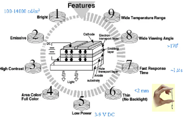
Fig. 1.1 The features of OLED panel…....………...……… 2
Fig. 1.2 (a) Basic multilayer structure of OLED (b) Engergy diagram of multilayer structure…....………...……… 3
Fig. 1.3 Schematic diagram for the photons coupled into three types of modes in OLED………..………… 4
Fig. 1.4 Schematic diagram for increasing the surface roughness of the substrate-air interface of an OLED panel……… 5 Fig. 1.5 Mesa geometry of microlens array on OLED panel………... 5
Fig. 1.6 Special geometry of microlens array on OLED panel……… 5
Fig. 1.7 Schematic for increasing the surface roughness of monolayers of silica spheres on the substrate of an OLED panel………...….…… 6
Fig. 2.1 Illustrative figure of the transmittance at the interface between top-glass substrate and air……….. 12
Fig. 3.1 Flow chart of ALEL fabrication process……… 14
Fig. 3.2 Semiconductor fabrication process of microoptical structure……… 15
Fig. 3.3 ALEL replication process flow (a) filling the mold with PDMS (b) removing bubbles by vacuum process, and (c) curing………..…….. 16
Fig. 3.4 Photograph of SEM……… 18
Fig. 3.5 Schematic diagram of Conoscope……….……….. 19
Fig. 4.1 Schematic diagram of OLED structure……….……….. 21
Fig. 4.2 Schematic diagram for organic layers of OLED structure………….…………. 21
Fig. 4.3 Schematic diagram for designing pixel size of light source and ALEL………. 22
Fig. 4.4 Schematic diagram of measurement………...……… 22
Fig. 4.5 Illustration of parameters for designing array light-enhancing layer………….. 23
Fig. 4.6 Illustration of the relationship between gain factor and TILT…..……….. 24
Fig. 4.7 Illustration of the relationship between gain factor and Height………..……… 25
Fig. 4.8 Definition of opening area ratio……….. 25
Fig. 4.9 Illustration of the relationship between gain factor and opening area ratio (transfromed from gain-TILT curve)……….. 26
Fig. 4.10 Illustration of the relationship between gain factor and opening area ratio (transferred by various height)………...………. 27 Fig. 4.11 Illustration of the relationship between gain factor loss and ALEL shif…….... 28 Fig. 4.12 Illustration of ALEL misalignment………..………... 29 Fig. 4.13 Schematic diagram of ALEL shift on X and Y axis (a) ideal case, (b) 30 µm,
(c) 60 µm, and (d) 90 µm……….………... 29 Fig. 5.1 PhotographS of fabricated structure on molds from optical microscope (a)
Different spacing between two adjacent pixels (b) Different pixel size………. 33 Fig. 5.2 Illustrations figure of fabricated structure on molds (a) hight of each ALEL
pixel (b) cross-section and crystal lattice direction of a silicon mold….……… 33 Fig. 5.3 A photograph of ALEL………...……… 34 Fig. 5.4 SEM photographs of ALEL……….…...……… 34 Fig. 5.5 Photographs of ALEL by optical microscope (a) tilt angle of ALEL pixel, (b)
various spacing between two adjacent pixels (c) various height between two ALEL pixel (d) various pixel size………..……….………… 35 Fig. 5.6 Photographs of measurement systems (a) Chromameter CS-100 and (b)
Conoscope………..……….……… 36 Fig. 5.7 Illustration of gain factor loss for various ALEL alignment cases (a)
alignment mark aimed at the center of ALEL pixel, (b) various alignment cases (c) the corresponding photographs from conoscope and gain factor………...……… 38 Fig. 5.8 Illustration of the relationship between gain factor and Height……….. 39 Fig. 5.9 Illustration of the relationship between gain factor and opening area ratio….... 40 Fig. 5.10 Illustration of the relationship between gain factor and pixel size……….…… 41 Fig. 5.11 Photographs of OLED panels with ALELs (a) CPT 7” OLED panel and (b)
‘X’ company 1.5” OLED panel………..………… 42 Fig. 6.1 The current manufacturing process and materials of BEF…………..………… 45 Fig. 6.2 The new pixel size design for ALEL………..…………..……..………… 46
List of Tables
Table 4.1 Gain factor of OLED panels with various microlens geometry……….……… 30 Table 5.1 Moire pattern between different alignment cases for comparison………..…… 37
Chapter 1
Introduction
1.1 Organic light-emitting diode (OLED) displays
With the popularization of computer, internet and wireless communication, display technology has been progressing rapidly from the last decade. As an interface between human being and information devices, electronic displays are required to process sufficient information content and be operated in various applications with different criteria, such as wide viewing angle, high contrast ratio, high brightness, high readability, high resolution, fast response time, portability, and high tolerance of environment variations. Cathode Ray Tubes (CRTs) techniques have been developed maturely and were superior in many aspects, except for its size, and power consumption. New displays, such as liquid crystal displays (LCDs), plasma display panels (PDPs) and organic light emitting diode (OLED) panels [1] were excellent in thin format, yet, at low cost. Among these candidates, organic light-emitting diodes (OLEDs) are the most potential to be the next generation planar light source and display devices.
Since multilayer OLED had been demonstrated by Tang and Vanslyke in 1987 [2], it has received much attention due to its many advantages, as illustrated in Fig. 1.1. Moreover, organic electroluminescence based on conjugated polymers was first discovered in 1990 by Burroughes et al. in Cambridge [3].
Fig. 1.1 The features of OLED panel.
The Schematic multilayer structure and energy diagram are shown in Fig. 1.2 (a) and (b). Hole and electron transporting layer (HTL and ETL, respectively) are sandwiched between the hole injecting anode and the electron injecting cathode, respectively. In the ETL, the mobility of electron and hole are much lower than that in the HTL. The ETL increases the steady-state majority-carrier density, reduces the number of hole being discharged nonradiatively at the cathode, and promotes electron injection by generating an internal space charge that redistributes the internal electric field. The injected electrons and holes migrate in opposite directions. About 75% of the recombination events yield the generally nonemissive triplet excitons, and ~25% the radiative singlet excitons, mostly at the HTL/ETL interface.
(a) n-type p-type
+
–
Recombination of electron and hole Junction Energy released by recombination + + + + — — — — — + Net flow of electrons light n-type p-type+
–
Recombination of electron and hole Junction Energy released by recombination + + + + — — — — — + Net flow of electrons light radiation (b)Fig. 1.2 (a) Basic multilayer structure of OLED [1] and (b) Engergy diagram of multilayer structure.
Both the intrinsic photoluminescence efficiency of the organic material and the output coupling efficiency of the sandwiched ITO/organic layers are related to the extraction efficiency. However, the output coupling efficiency remains about 20%. The photons emitted
in the active region of OLEDs are coupled into three types of modes: direct transmission into the air, the glass total internal reflection mode, and the high index (anode/organic) guided mode, as shown in Fig. 1.3. Assuming Lambertian light sources, the fractions of energy in the three modes have been estimated as 20 %, 30 %, and 50 %, respectively [4]. Light emitted outside of a narrow escape cone suffers total internal reflection (TIR) and waveguiding within the device active layers. Hence almost 80 % of the generated light is lost in the glass
Fig. 1.3 Sch substrates.
ematic diagram for the photons coupled into three types of modes in
1.2 Methods to increase light efficiency of OLED displays
Many methods were employed to overcome efficiency limitations by suppressing the wav
C. F. Madigan,Appl. Phys. Lett. 76,2000
Total internal reflection mode High_index guided mode n =1 n =1.5 n =1.8 n =1.75 20% 30% 50% External mode
C. F. Madigan,Appl. Phys. Lett. 76,2000
Total internal reflection mode High_index guided mode n =1 n =1.5 n =1.8 n =1.75 20% 30% 50% 20% 30% 50% External mode
Anode
OLED [4].eguide modes. The methods of rough or textured surfaces [5][6], mesa structures, and lenses [7][8] are shown in Figs. 1.4, 1.5 and 1.6. While these structures are applied on an OLED panel, the incident angle is turned to be smaller than critical angle, and then the TIR effect is eliminated. The maximal improvements of the luminance efficiency are about 50 % ~ 56 %.
Fig. 1.4 Schematic diagram for increasing the surface roughness of the substrate-air interface of an OLED panel [5].
S. Moller, 2002
Mesa cone geometry
Fig. 1.5 Mesa geometry of microlens array on OLED panel [7].
Spherical geometry
Mao-Kuo Wei, 2004
The methods utilized to improve LED outcoupling have also been applied to OLEDs. Recently, two dimensional photonic crystals are reported to enhance the outcoupling of light along the surface normal [9][10]. The incorporation of monolayers of silica spheres with diameters of 550 nm as a scattering medium in a device, or the positioning of these monolayers on the substrate, also enhanced light output [11], as shown in Fig. 1.7. A corrugated substrate increased the light output by a factor close to 2 by Bragg scattering in the forward direction for polymer LEDs [12]. Tsutsui et al. showed that the external quantum efficiency can be doubled by incorporating a thin layer of a very low refractive index silica aerogel (n =1.03) in the device [13]. Furthermore, the thickness of the ITO layer has been controlled in order to reduce the energy loss in the high-index layer [14].
Fig. 1.7 Schematic for increasing the surface roughness of monolayers of silica spheres on the substrate of an OLED panel [11].
1.3 Motivation and objective of this thesis
For the applications of microlens arrays on self-emitting devices, little work has been done on systematical analysis. Additionally, among these technologies, the pyramidal array light-enhanced layer (ALEL) is easier fabricated and has been widely applied in many fields.
Therefore, our objective is to study the pyramidal ALEL design rule on an OLED panel to obtain higher light efficiency than that of prior arts.
The optical properties of the pyramidal ALEL on OLED panel are modeled by a ray tracing calculation, which predicts an increase of light efficiency by a gain factor to compare with an OLED panel without ALEL. Then, the characteristics and performance of the fabricated structure, such as similarity to the geometric design and light efficiency were measured by typical semiconductor measurement systems, such as optical microscope (OM), scanning electron microscope (SEM), chromameter, and conoscope.
1.4 Organization
The thesis is organized as follows: the principles and the features of the array light-enhanced layer and OLED panel will be presented in Chapter 2. In Chapter 3, the considerations of the fabrication technologies to realize the array light-enhanced layer are summarized. The major measurement equipments used to characterize the fabricated the array light-enhanced layer are illustrated. In Chapter 4, the simulated results including light enhancement, and various parameters of ALEL used to verify and optimize our design will be presented. In Chapter 5, the experimental results including several fabricated samples are demonstrated. Based on the measurement results, several critical parameters in fabrication process are discussed, and then the desired structure will be realized and modified. In
Chapter 2
Principle
2.1 Introduction
The output coupling loss, one of various efficiency loss mechanisms of an OLED, has been introduced in devices. The potential for further improvements are also described.
The first loss process of various efficiency loss mechanisms of an OLED occurs due to that the charge carriers do not recombine in the organic layer to produce excitons. It is commonly referred as the charge balance, which is defined as γ, the probability of the balance between the number of positive and negative charges injected into the organic layer. The excitons formed of two types, singlets that have a radiative decay, triplets that decay through nonradiative processes, lead to efficiency loss. The ratio of singlets to triplets will be defined as γst. Another efficiency loss, the intrinsic photoluminescence efficiency of the organic
material, is defined a quantity q. A large portion of the light generated in the device is unable to couple out. The loss is defined as ηc.
These four major losses described above can be combined to determine the external quantum efficiency (ηext) of OLED device, using (1)
(1)
2.2 Optical output coupling
A brief description is provided for the models that have been developed to calculate the output coupling of OLEDs. Models based on calculating the interference effects are due to emitted and reflected beams [15][16] to classical [17] [18].
2.2.1 Total internal reflection and trapped light
The large mismatch between the refractive index of the organic layers, glass substrate and air results in a large proportion of the light rays undergoing total internal reflection as lights pass from a high to a low refractive index material. Only light emitted at an angle smaller than the critical angle can escape from the surface, while all other light is internally reflected back into the device. The light trapped within the device will be waveguided, either absorbed or emitted from the edge of the substrate.
A simple expression can be derived for the maximum emission efficiency based on ray optics and Snell’s law. Cathode is set as a perfect reflector and the emission is isotropic distribution. Then, the output coupling efficiency is given by the relationship [19],
(2)
For emission from in-plane dipoles, the proportion of light travelling perpendicular to the surface is increased and thus light is emitted at angles smaller than the critical angle, the expression for the light out coupling approximates to the following
(3)
In small molecule-based OLEDs, there is no preferential arrangement of the dipoles and the emission is thus expected to be isotropic. However, in polymer based OLEDs, the polymer chains are found to be aligned preferentially in-plane [15][20][21] which leads to increase output coupling. A useful indication of the magnitude of the loss in efficiency due to poor light output coupling of the photons generated in the device could be obtained by using this simple model. Based on a typical value of the refractive index of n = 1.7, the output coupling is predicted to be only 17 % for isotropic emission and 26 % for in-plane emission.
2.2.2 Modeling of output coupling
To produce accurate modeling of the output coupling, the structures of OLEDs need to be taken into consideration. A typical OLED device consists of four major components, the cathode, organics layer where the light is generated, transparent ITO contact layer, and the glass substrate. The refractive indexes of the organic layer (n = 1.6 ~ 2.0 ), the ITO (n = 1.6 ~ 2.0 ) and the glass (n = 1.5 ) are larger than the air, which leads to three types of modes: direct transmission into the air, the glass total-internal-reflection mode, and the high index (ITO/organic) guided mode. These will either be absorbed by the various layers, emit from the edge of the substrate, or be reflected at other interfaces in the device. Thus, high efficiency requires the minimization of these modes.
Ji-Seon et al. [16] describes an optical model for the emission from a polymer-based OLED. The study includes the transmission through the various layers with appropriate values used for the complex refractive index of an actual device and takes into consideration the effect of interference from the metal cathode. The angular dependence of the emission intensity from the devices is also used to predict the output coupling in this model. An experimental relation is calculated for the output coupling ratio as a function of the refractive index of the organic layer,
(4)
for isotropic emitting dipoles and
(5)
for in-plane emitting dipoles.
For the refractive index of the organic layer (n = 1.7 ), the maximum output coupling based on the optimum location of the emission zone in the organic layer for isotropic and in-plane
dipoles corresponds to a value of 26 % and 42 %, respectively.
The out-coupling and emission spectrum is a function of the location of the recombination zone by considering the strong interference from the metal cathode. In addition, proximity of the emission zone to the metal results in the quenching of the luminescence at cathode, due to energy transferring to the metal [17][20]. Thus, the locating of the recombination zone away from the metal cathode and the constructive interference of the emitted and reflected light are optimized to obtain the maximum output coupling [15].
2.2.3 Fresnel equations
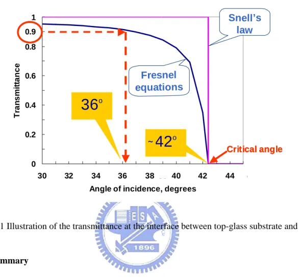
A more rigorous analysis by a simulation tool with the Fresnel equations assigned should be used to perform the simulation. We analyzed the transmittance at the interface between the top-glass substrate and the air. According to Fresnel equations, the coefficients of refraction for p-ray and s-ray, rpp and rss, satisfy:
r n n n n r n n n n pp t i i t i i ss i i t t i i t = − + = − + cos cos cos cos cos cos cos cos θ θ θ θ θ θ θ θ t t t (6) (7)
where θi, θt, ni and nt, are denoted as the incident angle, the refractive angle, the
refractive index of the first medium and that of the second medium, respectively. Assume there is no loss in the mediums, the transmittances of p-ray and s-ray, then, can be derived as Tp=1-|rpp|2 and Ts=1-|rss|2, respectively. Practically, only the average transmittance, T=(Ts+
Tp)/2, will be measured in the experiment. The refractive index of top substrate was set as 1.46. The results, as illustrated in Fig. 2.1, show that the transmittance will decrease to less than 90%, when the incident angle is larger than 36 degrees. However, the critical angle
Fresnel equations is necessary for establishing an appropriate pyramidal-ALEL model.
Transmittance versus incident angle
0 0.1 0.2 0.3 0.4 0.5 0.6 0.7 0.8 0.9 1 30 31 32 33 34 35 36 37 38 39 40 41 42 43 44 45 Angle of incidence, degrees
T ra n s m itta n c e Critical angle
42
o Critical angle Critical angle42
o36
o Fresnel equations Snell’s law ~Fig. 2.1 Illustration of the transmittance at the interface between top-glass substrate and air.
2.3 Summary
A simple expression can be derived for the maximum emission efficiency based on ray optics and Snell’s law. Cathode can be set as a perfect reflector and the emission can be isotropic distribution. For the typical value of refractive index of the organic layer (n = 1.7), the maximum output coupling efficiencies for isotropic and in-plane dipoles correspond to a value of 26 % and 42 %, respectively [15]. Although, the critical angle analyzed from Snell’s law at the interface between the top-glass substrate and the air is about 42 degrees, the incident angle larger than 36 degrees causes the transmittance less than 90 % from Fresnel equations. Therefore, considering the Fresnel equations is necessary for establishing a simulation model of the appropriate pyramidal-ALEL.
Chapter 3
Fabrication and Measurement Instruments
3.1 Introduction
A preliminary structure will be used to confirm the features of the microlens array. The embodiment including several fabrication processes will be shown in the following sections, and all the fabrication process, technologies, instruments and a preliminary structure will be introduced in this chapter.
First, the semiconductor fabrication process including mask layout, spin coating, exposure and development were preceeded. Besides, the mold was subsequently filled with the thermal-cured elastomer to replicate the microlenses. Then, the characteristics and performance of the fabricated structure, such as similarity to the geometric design and light efficiency were measured by typical measurement systems, such as optical microscope (OM), scanning electron microscope (SEM), chromameter, and conoscope. The major features of the above mentioned instruments will be illustrated in this chapter.
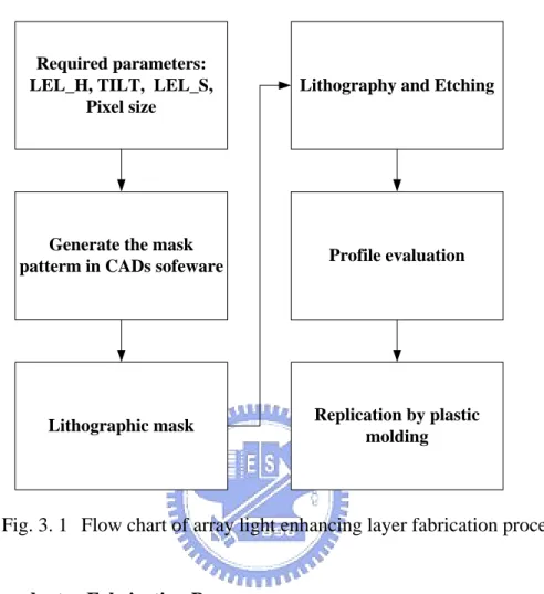
3.2 Fabrication Process
The entire fabrication processes we utilized to fabricate the microoptical components include the typical VLSI fabrication processes and plastic modeling replication techniques.
First, we determined the feature parameters, like the height of each ALEL pixel (LEL_H), the tilt angle of pyramidal pixel (TILT) and the spacing between two adjacent pixels (LEL_S), need to be designed properly for practical component fabrication. Then, we transfer the desired structures into multi-pattern for mask layout. Third, the microoptical structure on
microoptical structure into thermal-cured elastomer to replicate the microlenses. The processes are shown schematically in Fig. 3.1.
Required parameters: LEL_H, TILT, LEL_S,
Pixel size
Generate the mask patterm in CADs sofeware
Lithographic mask
Lithography and Etching
Replication by plastic molding
Profile evaluation
Fig. 3. 1 Flow chart of array light enhancing layer fabrication process.
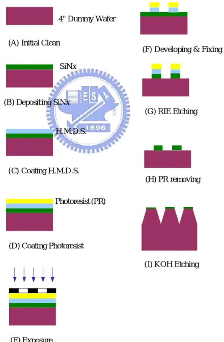
3.2.1 Semiconductor Fabrication Process
A prototype is fabricated to characterize the features of the microlens array structure. The semiconductor processes including cleaning, coating PR, UV exposure with G-Line (436 nm) stepper, develop, fixing, RIE etching and KOH etching will be proceeded to fabricate the desired structure on Si-wafer at semi-conductor research center (SRC).
The detail processes are shown in Fig. 3.2. First step is initial-cleaning. Wet-cleaning processes are necessary to obtain an ultra clean wafer surface for subsequent fabrication. Then a 0.5 µm thick layer of SiNx will be deposited by plasma enhanced chemical vapor on wafer. Next, the wafer is placed on a vacuum chuck in the coater and the photoresist is dropped onto the center of the wafer. A uniform and thin photoresist layer can be coated on the wafer
surface after spinning the wafer. The following step is exposure. The mask pattern is transferred onto the wafer. The exposed wafer is loaded into the development system after exposure. Consequently the desired structure will show up in the photoresist. Etching is then applied to get the desired structures from the developed pattern to a wafer. Non-photoresist-covered SiNx will be removed during RIE etching. Then the remained photoresist will be stripped by acetone. Finally, the regions of silicon will be etched by KOH and the fabricated microoptical structure will appear on the Si wafer.
(A) Initial Clean
H.M.D.S.
(C) Coating H.M.D.S. SiNx
(B) Deposit ing SiNx
Photoresist (PR)
(D) Coating Photoresist
(F) Developing & Fixing
(G) RIE Etching
(H) PR removing
(E) Exposure
(I) KOH Etching 4" Dummy Wafer
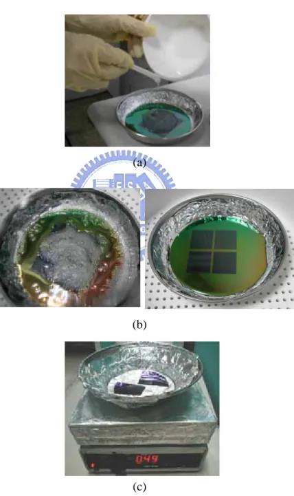
3.2.2 Replication
The plastic material for replication is considered to have a similar refraction index as optical glass. We use poly(dimethylsiloxane) (PDMS), a thermal-cured elastomer, as the material. Fig. 3.3 shows an overview of the major replication technology.
(a)
(b)
(c)
Fig. 3.3 ALEL replication process flow (a) filling the mold with PDMS (b) removing bubbles by vacuum process, and (c) curing.
The fabricated mold was pretreated by an anti-sticking layer (1H, 1H, 2H, 2H-perfluorodecyl trichlorosilane) to prevent the mold adhering to PDMS during the replication process. To fabricate the microlenses, the mold was subsequently filled with PDMS. Then we remove the bubbles from the microstructure by using vacuum chamber. The PDMS is cured at 50 °C for 3 hr leading to a flexible sheet that can easily be peeled off from the mold. The thickness of the PDMS layer ranges from 1 to 3 mm.
3.3 Measurement System
After the fabrication, we must make sure the fabricated components meet the design goal. First, the geometric similarity to the designed structure is checked by the optical microscope (OM) and scanning electron microscope (SEM). Then, the optical performances of the fabricated components and designed ALEL on OLED panel are measured by the chromameter CS-100 and conoscope system, the detailed descriptions are shown below.
3.3.1 Scanning Electron Microscope (SEM)
A scanning electron microscope (SEM) is an essential instrument to measure the accuracy and fidelity of the fabricated microstructure, as shown in Fig. 3.4. The instrument scans electrons reflecting onto a fluorescent screen across the target where the image is captured by a camera and enlarged. Electrons are much smaller than atoms, so a scanning electron microscope paints a razor-sharp image of the target, and the feature variation of few angstrom can be observed. SEM is useful for mapping details of objects that optical microscopes can not resolve. Using the electromagnetic lenses to focus the accelerated electron beam, the diameter of electron beam can be converged to the dimension of 10 µm. The secondary electrons are generated where the focused accelerated electrons bombard the sample. Detecting the secondary electrons can determine the location of bombardment. Simultaneously, the focusing electron beam scans the surface of sample, with the aid of
scanning coil, to map the feature of measured area.
HITACHI S-4000 SEM was utilized to measure the quality of our fabricated microstructure elements. The line width, etching depth, and aperture size can be measured accurately.
Fig. 3.4 Photograph of SEM.
3.3.2 Measurement Systems for light efficiency
3.3.2.1 Chromameter CS-100
The color and brightness of image are the important properties of system we want to evaluate. In order to get these information, a colormeter is necessary. We choose the Minolta Chroma Meter CS-100, which utilizes three high-sensitivity silicon photo cells, which are filtered to match Commission International de I’Eclairage (CIE) standard observer response. Chromaticity coordinates (x,y) and illumination (Y) as well as color temperature in Kelvin (K) are calculated from the three cells’ measurements. With this compact reliable color analyzer, we can easily get the Chromaticity coordinates and
3.3.2.2 Conoscope
Conoscope is a measurement system which utilizes Fourier transform lens to transfer the light beams emitted (or reflected) from the test area of different angles to the CCD array, as shown in Fig. 3.5. Every light beam emitted from the test area with a θ incident angle will be focused on the focal plane at the same azimuthal angle and at a position x = F(θ). Therefore, the angular characteristics of the sample are thus measured simply and quickly, without any mechanical movement. Particularly, which kind of light source, i.e. collimated or diffuse illumination, is provided depending on the needs.Besides, by equipped with a fast photometer system and a high-sensitivity spectrometer, its functions are extended to comprise not only the simultaneous measurement of luminance and chromaticity versus viewing direction, evaluation of the data yields, i.e. luminance contras ratio, grey-scale inversion and reduction, color shift and many more characteristics, but also the spectra and temporal luminance variances.
C: cone of converging elementary parallel beams A: variable aperture
Chapter 4
Simulated Results and Discussions
4.1 Introduction
In chapter 2, we had analyzed the transmittance at the interface between the top-glass substrate and air to confirm that the Fresnel equations are necessary for modelling a pyramidal ALEL. We established a simulation model to characterize the features of the array light-enhancing layer on OLED panel.
First, the parameters of pyramidal ALEL, including the height of each ALEL pixel, the tilt angle of pyramidal pixel and the spacing between two adjacent pixels, were designed and optimized. After that, the alignment issue of the array light-enhancing layer on OLED panel was also discussed.
4.2 Simulation Software
The optical simulator Advanced Systems Analysis Program (ASAPTM
), developed by Breault Research Organization (BRO) was used to optimize the array light-enhancing layer on OLED panel and simulate its light efficiency.
4.3 Simulation description
4.3.1 Optical Model
In order to consider the whole effect of the array light-enhancing layer on an OLED panel, all the design and optimization were carried out under the complete system framework.
bottom glass substrates, as shown in Fig. 4.1. Ribs and insulators were set with 60 % transmittance. Since the organic layers, including the electron injection layer, the electron transport layer, the active layer (the emitting layer), the hole transport layer and the hole injection layer, are much thinner (~0.15 µm) than other layers, they are assumed as one “source layer” in our simulation, as shown in Fig. 4.2. Metal cathode was set with 90 % reflectance.
Fig. 4.1 Schematic diagram of OLED structure.
Glass Substrate
Cathode
Electron Transport Layer Electron Injection Layer
Hole Transport Layer Hole Injection Layer
Anode
Emitting Layer
Organic Layers
Lights from active layer was assumed to emit in the form of pixel array and was set as an isotropic light source. The array light-enhancing layer consists of the base substrate and microlens array. The pixel size of ALEL, as shown in Fig. 4.3, was set to fit one of OLED panel. The size of ALEL and OLED panel are W×L. In addition, a flat detector with the diameter of 3cm was located at a distance of 3.5cm above the OLED panel, as shown in Fig. 4.4.
1 Pixel size of
OLED Panel
1 Pixel size of
OLED Panel
1 Pixel size of
ALEL
1 Pixel size of
ALEL
Alignment
Fig. 4.3 Schematic diagram for designing pixel size of light source and ALEL.
L OLED panel ALEL W Detector 3 cm
Fig. 4.4 Schematic diagram of measurement.
Light efficiency is defined as the detected flux over the generated one. Furthermore, gain factor was defined as the ratio of the light efficiency of an OLED panel with ALEL to that of a panel without ALEL, which were served as the bases of the optimizations.
(1) = detected flux light efficiency generated flux d = etected flux light efficiency generated flux ……… (2) light efficiencyof OLED panel with ALEL
Gain Factor =
light efficiencyof OLED panel
light efficiencyof OLED panel with ALEL Gain Factor
light efficiencyof OLED panel
=
4.3.2 Parameters
In order to obtain to maximum gain factor, several variables, as shown in Fig. 4.5, such as the height of each ALEL pixel (LEL_H), the tilt angle of pyramidal pixel (TILT) and the spacing between two adjacent pixels (LEL_S), need to be designed properly. A simulation tool, ASAPTM
, with the Fresnel equations assigned was used to perform the following simulation.
LEL_H TILT LEL_S Microlens array Substrate
Fig. 4.5 Illustration of parameters for designing array light-enhancing layer.
4.4 Results and discussions
4.4.1 Tilt angle and spacing of pyramidal pixel
First, the relationship between the gain factor and the tilt angle (TILT) will be discussed. Height and spacing are kept constant, and TILT is changed from 90° to the minimum angle where the two slopes meet at the intersection point, and then the relationship between the gain factor and TILT is formed. Besides, spacing is kept as different constants to represent the
relationship between the gain factor and spacing. The green sub-pixel light source is turned on. From the simulated results, as illustrated in Fig. 4.6, the maximal gain factor can be derived at 50° to 55° and smaller spacing.
1.0
1.2
1.4
1.6
1.8
2.0
40
50
60
70
80
90
TILT (degrees)
Ga
in
Fa
c
to
r
Spacing = 10 µm Spacing = 25 µm Spacing = 40 µmFig. 4.6 Illustration of the relationship between gain factor and TILT. The height is 125 µm.
4.4.2 Height of pyramidal pixel
Next, the relationship between the gain factor and the height is discussed. From the simulated results, as illustrated in Fig. 4.7, the curve of gain factor becomes stable when the height is higher than 100 µm. Since the lower height can bring higher yield rate during the demolding process, the optimized height is set as around 150 µm.
1.0
1.2
1.4
1.6
1.8
2.0
0
50
100
150
200
250
Height (µm)
G
a
in
F
acto
r
TILT = 40 TILT = 50 TILT = 60 o o oFig. 4.7 Illustration of the relationship between gain factor and Height. The spacing is 10 µm.
4.4.3 Opening area ratio
We further broaden the analysis of the relationship between gain factor and the parameters of ALEL. Opening area ratio is defined as the sum of the flat areas A over the pixel size of ALEL, as illustrated in Fig. 4.8.
The relationship between the gain factor and the parameters of ALEL, as illustrated in Figs. 4.6 and 4.7, will be transferred to the relationship between the gain factor and the opening area ratio.
First, the relative curves of gain factor versus opening area ratio are obtained by converting the gain-TILT curve (Fig. 4.6). Maximal opening area ratios, as illustrated in Fig. 4.9, are different at various spacing. Therefore, the relationship between the gain factor and TILT is still the suitable method to obtain proper directionalities.
1.0
1.2
1.4
1.6
1.8
2.0
0
20
40
60
80
100
Opening area ratio (%)
G
a
in
F
acto
r
Spacing= 10 µm Spacing= 25 µm Spacing= 40 µmFig. 4.9 Illustration of the relationship between gain factor and opening area ratio (transfromed from gain-TILT curve). The height is 125 µm.
Moreover, the relationship between gain factor and height was also transferred to the relative curves of gain factor versus opening area ratio. From the results, as illustrated in Fig. 4.10, it can be concluded that smaller opening area ratio produces higher gain factor. In addition, the gain factor is similar when opening area ratio is smaller than 30 % at the optimized TILT angle of 50°. It could be the reference for designing lower height of ALEL to bring higher yield rate during the demolding process.
1.0
1.2
1.4
1.6
1.8
2.0
0
20
40
60
80
100
Opening area ratio (%)
Ga
in
Fa
c
to
r
TILT = 40 TILT = 50 TILT = 60 o o oFig. 4.10 Illustration of the relationship between gain factor and opening area ratio (transferred by various height). The spacing is 10 µm.
4.4.4 Alignment issue
In our design, the pixel size of ALEL is set to fit the one OLED pixel. As a result, the alignment issue should be considered in the mass production. Fig. 4.11 shows the result of gain factor loss versus ALEL shift. ALEL shift is defined as the same shift on X and Y axes as illustrated in Fig. 4.12. The space between adjacent sub-pixels on OLED panel is about 40 µm. When ALEL are 60 µm and 90 µm shifted, as illustrated in Figs. 4.13 (c) and (d), their regions of the pixel spacing of ALEL crossing the green sub-pixel source are similar. There is about 15 % loss of gain factor when ALEL is shifted 90 µm along X and Y axis. The gain factor losses of 60 µm and 90 µm misalignments are also approximated. Therefore, the pixel
Fig. 4.11 Illustration of the relationship between gain factor loss a spacing of ALEL crossing light source is the main factor of alignment.
nd ALEL shift.
0
5
10
15
20
25
0
30
60
9
X & Y Shift (µm)
Ga
in
Fa
c
to
r L
o
ss (
%
)
Spacing = 40 µm , TILT = 55 Height =125 µm, o0
OLED panel ALEL
Y
X
OLED panel ALELY
X
Fig. 4.12 Illustration of ALEL misalignment.
Pixel spacing
(a) (b) (c) (d)
Fig. 4.13 Schematic diagram of ALEL shift on X and Y axis: (a) ideal case, (b) 30 µm, (c) 60 µm, and (d) 90 µm.
4.5 Comparison
The structures of the other two prior arts, as illustrated in table 4.1, are listed here for comparison. The dimension of our proposed ALEL pixel was about 300 µm, which fitted the pixel of light source. Other variables were determined by optimized results and process limitation. The optimal pixel spacing was equal to Dr. Wei’s result and the height was larger than the other two prior arts. As a result, the gain factor of our proposed structure is as high as 1.70.
Table 4.1 Gain factor of OLED panels with various microlens geometry.
Journal OPTICS EXPRESS,Mao-Kuo Wei, No 23, Vol. 12, 2004
S. Moller, J. Appl. Phys.,
V9, 2002
NCTU
Spherical geometry Arc geometry pyramid-shaped geometry (55o)
Microlen Dimension (µm) 100 10 ~ 300
Pixel Spacing (µm) 11 ~ 0 15
Height (µm) 50 5 200
ALEL Material PMMA PDMS PDMS
Gain factor
1.56
1.50
1.70
Structure4.6 Summary
We have designed and optimized the array light-enhancing layer on an OLED panel. From the mentioned analyses, thus the structure of ALEL has the distinguished capability to eliminate the total internal reflection (TIR) effect, thus, light efficiency and gain factor of OLED panel can be increased significantly. Optimized pyramidal ALEL yields a gain factor of 1.7. A pyramidal ALEL on OLED panel produces higher light efficiency than other structures in our simulation results.
Additionally, according to the simulated results, three important features of design rules for ALEL on OLED panel can be derived:
In ideal alignment cases, the gain factor can be optimized with (a) Narrower pixel spacing
(b) Tilt angle of 50º to 55º
(c) Opening area ratio smaller than 30 %.
For alignment issue, the area of pixel spacing cross light source was the main factor of the gain factor loss.
Chapter 5
Experimental Results and Discussions
5.1 Introduction
Based on the simulation and fabrication presented in the previous chapters, the experimental results and discussions will be shown in this chapter. Optical microscope (OM) and SEM were utilized to examine the mold and ALEL. The optical performances of a Chung Hwa Picture Tube, Ltd (CPT) OLED panel with ALEL, such as luminance, were measured by Chromameter CS-100 and Conoscope. Finally, the gain factors of ALEL-attached OLED panels with two different pixel sizes are compared.
5.1.1 Mold examination
Optical microscope was used to examine the fabricated structures of silicon mold. The spacing between two adjacent pixels and the pixel size were checked, as illustrated in Figs. 5.1 (a) and (b). The height (H) of each ALEL pixel was also inspected as illustrated in Fig. 5.2 (a). Wet etching rate on the {111} crystal lattice direction, as illustrated in Fig. 5.2 (b), is 400 times slower than the {100} direction [22]. Since the angle between {100} and {111} crystal lattice is well-know as 54.74º, which fits our optimized TILT, the relationship between the height of the ALEL pixel (H) and the width of the slope (W) can be derived by the following equation:
Spacing between two adjacent pixels
15 µm 40 µm
(a)
Pixel size
Pixel size of ALEL : Pixel size of OLED panel1:1 0.5 : 1 0.2 : 1
(b)
Fig. 5.1 Photographs of fabricated structure on molds from optical microscope (a) different spacing between two adjacent pixels and (b) different pixel size.
Height of ALEL pixel
W H H = W tan (54.74º ) W H
{111}
{100 }
54.74 o Si-mold{111}
{100 }
54.74 o Si-mold (a) (b)Fig. 5.2 Illustrations of fabricated structure on molds from optical microscope (a) height of ALEL pixel and (b) cross-section and crystal lattice direction of a silicon mold.
5.1.2 Replication examination
Optical microscope and SEM were used to examine the replicated ALEL. The overviews of ALEL are shown in Figs. 5.3 and 5.4, while various variables of ALEL are illustrated in Fig. 5.5.
Fig. 5.3 A photograph of ALEL.
~
Tilt angle of pyramidal pixel
TILT
TILT ~~
Tilt angle of pyramidal pixel
TILT TILT
(a)
LEL_S LEL_S
Spacing between two adjacent pixels
15 µm 30 µm 40 µm
(b)
(d)
Fig. 5.5 Photographs of ALEL by optical microscope (a) tilt angle of ALEL pixel, (b) various spacing between two adjacent pixels, (c) various height of two ALEL pixel, and (d) various pixel size.
Height of ALEL pixel
LEL_H LEL_H LEL_H (c) 50 µm 100 µm 150 µm 200 µm Pixel size Pixel size Pixel size 0.2 : 1 0.5 : 1 1:1 Pixel size of ALEL : Pixel size of OLED panel
5.1.3 Measurement System
The measurement system was illustrated in Fig. 5.6. The optical performance, the luminance of ALEL region at the direction normal to CPT OLED panel, was measured by Chromameter CS-100 and Conoscope in a dark room.
Detector
( MINOCTA Chroma Meter CS-100 )
OLED Panel (CPT)
Power Supply
Detector
( MINOCTA Chroma Meter CS-100 )
OLED Panel (CPT) Power Supply (a) Detector (Conoscope) (b)
Fig. 5.6 Photographs of measurement systems (a) Chromameter CS-100 and (b) Conoscope.
5.2 Results and discussions
5.2.1 Alignment issue
5.2.1.1 Moire pattern
According to the measured luminance, we studied the alignment issue first. Several alignment cases, as illustrated in table 5.1, are listed here for comparison. Free from moire pattern is the desired optical performance as shown in the left alignment of the case 1. Moire pattern are serious in the cases 2 and 3. We checked the periods of pixel size of ALEL and the pixel size of the OLED panel, they were different along x and y axes. Therefore, the experimental results show that when one ALEL pixel fitting with one OLED pixel and without rotational misalignment, both ALEL shifts along x and y axes are allowed for the OLED panel to be free from moiré pattern.
Table 5.1 Moire pattern between various alignment cases for comparison. Alignment Image Moire Pattern
No
Yes
Yes
OLED Panel ALELNo
Yes
Yes
Image Moire Pattern
OLED Panel ALEL OLED Panel ALEL
(1)
(2)
(3)
5.2.1.2 Gain factor loss
According to the experimental results of gain factor loss, larger cross region of pixel spacing and light source caused a lower gain factor, as illustrated in Fig. 5.7. Hence, the area of pixel spacing of ALEL cross the light source of OLED panel was the dominant factor in alignment, so called the pixel spacing effect in this thesis.
(a)
(b)
(c)
Fig. 5.7 Illustration of gain factor loss for various ALEL alignment cases (a) alignment mark aimed at the center of ALEL pixel, (b) various alignment cases (c) the corresponding photographs from conoscope and gain factor. The luminance of the OLED panel measured by chromameter CS-100 was 55 cd/cm2. Gain factor 1.95 Gain factor 1.62 Gain factor 0.93
5.2.2 Height and pixel spacing of pyramidal pixel
n
and simulated results. Besides, the relative curves can be transferred to the relationship between gain factor and opening area ratio, as illustrated in Fig. 5.9. As the results, thesmaller opening area ratio can provide a higher gain factor, which agrees with the simulated result.
Fig. 5.8 Illustration of the relationship between gain factor and Height. The tilt angle is 55o. The relationship between gain factor and height, as illustrated in Fig. 5.8, was the studied for ideal alignment. The tendencies of relative curves are similar in both experimental
0.8
1.0
1.2
G
1.4
1.6
1.8
2.2
0
50
100
150
200
250
Height (µm)
a
in
F
acto
r
2.0
Spacing = 15 µm Spacing = 30 µm Spacing = 40 µm Spacing = 15 µm Simulation result1.0
1.2
1.4
1.6
1.8
2.0
2.2
0
10
20
30
40
50
60
70
Opening area ratio (%)
G
a
in
F
acto
r
Spacing = 15 µm Spacing = 30 µm Spacing = 40 µmFig. 5.9 Illustration of the relationship between gain factor and opening area ratio. The tilt angle is 55o.
5.2.3 Pixel size of pyramidal pixel
In addition, the relationship between gain factor and pixel size of ALEL, as illustrated in Fig. 5.10, was investingated. From the results, the case of the pixel size of ALEL equal to the pixel size of OLED panel obtained the maximal gain factor, and the pixel spacing effect appeared in the smaller pixel size of ALEL.
0.8
1.0
1.2
1.4
1.6
1.8
2.0
10
60 110 160 210 260 310 360 410
the pixel size of ALEL (µm)
Ga
in
F
ac
tor
Spacing = 40 µm TILT = 55 oPixel size of ALEL : Pixel size of OLED panel = 1:1
Pixel Spacing Effect Pixel Spacing Effect pixel size of OLED panel pixel size of OLED panel pixel size of ALEL pixel size of ALEL
5.3 Comparison
For comparison, two OLED panels with ALELs were demonstrated in Fig. 5.11, and the CPT OLED panel with the optimized ALEL showed a gain factor of 2.03, which was based on the process limitation. Because the pixel size of ALEL was different from that of X company, pixel spacing effect would cause more serious moire patterns and larger gain factor loss on X company’s OLED panel.
Fig. 5.11 Photographs of OLED panels with ALELs (a) CPT 7” OLED panel and (b) ‘X’ company 1.5” OLED panel.
‘X' company 1.5” OLED
Panel
Gain factor1.05
OLED Panel ALEL
CPT 7” OLED
Panel
Gain factor2.03 OLED Panel ALEL ALEL Spacing = 15 µm Height = 200 µm TILT = 54.7o
CPT 7” OLED
Panel
Gain factor2.03 OLED Panel ALEL ALEL Spacing = 15 µm Height = 200 µm TILT = 54.7o
5.4 Summary
The experiments, including ALEL fabrication, measurements from Chromameter and Conoscope, were implemented and successfully demonstrated the improvements of luminance and angular distribution of the proposed ALEL, designed for the CPT OLED panel. Based on one pixel size of ALEL fitting one pixel size of OLED panel, ALEL shifts along x and y axes are allowed for the OLED panel to be free from moiré pattern. Meanwhile, the measured results of several alignment cases were investigated and explained as the pixel spacing effect. According to the experimental curves of gain factor versus variables of ALEL, the higher luminance efficiency correlates to smaller opening area ratio, narrower pixel spacing, which agrees with the simulated results. Furthermore, the CPT OLED panel with the optimized pyramidal ALEL yields a gain factor of 2.0.
Chapter 6
Conclusions and future work
hancing layer designed for on CPT OLED panel was proposed and successfully demonstrated. In simulations, we analyzed the transmittance at the interface between the top-glass substrate and air to confirm that the Fresnel equations are necessary for modelling a pyramidal ALEL. Several important features of design rules for ideal ALEL alignment on OLED panel can be derived from the results:
(a) smaller opening area ratio (b) narrower pixel spacing (c) tilt angle of 50º~55º.
Optimized pyramidal ALEL yields a gain factor of 1.7 which produces higher light efficiency than other structures in our simulation results. For alignment issue, the area of pixel spacing cross light source was the main factor of the gain factor loss (pixel spacing effect).
The entire fabrication processes we utilized to fabricate the ALEL include the typical
material, p S), for replication is considered to have a similar refraction index as optical glass. As a result, based on one pixel size of ALEL fitting one pixel size of OLED panel, ALEL shifts along x and y axes are allowed for the OLED panel to be free from moiré pattern. Meanwhile, the measured results of several alignment cases were investigated and explained as the pixel spacing effect. According to the experimental results of gain factor versus variables of ALEL, the higher luminance efficiency correlates to smaller
6.1 Conclusions
The pyramidal array light-en
semiconductor fabrication processes and plastic modeling replication techniques. The plastic oly-dimethyl-siloxane (PDM
opening area ratio, narrower pixel spacing, which agrees with the simulated results. OLED panel with the optimized pyramidal ALEL yields a gain factor of 2.0. From
red by UV light simultaneously. Thereafter the UV-gel-coated substrate is peeled off from the roller and then the prisms are formed. The materials are considered for high throughput and yield rate of mass production. The future work is to replicate the ALEL by various thicknesses of PET and various recipes of UV gel and to evaluate improvements of luminance efficiency of the PET-based ALEL on CPT OLED panel.
Fig. 6.1 The current manufacturing process and materials of BEF. Furthermore, the CPT
the mentioned analyses, the structure of ALEL has the distinguished capability to eliminate the total internal reflection effect, thus, light efficiency and gain factor of OLED panel can be increased significantly.
6.2 Future work
6.2.1 New ALEL fabrication process
A fabrication process to manufacture brightness enhancing film(BEF) is as illustrated in Fig.6.1. The thin film of UV gel coated on a polyethylene terephthalate (PET) substrate is pressed by a roller with microstructures and cu
Polyethylene terephthalate (PET)
UV gel
Brightness Enhanced Film (BEF)
Polyethylene terephthalate (PET)
UV gel
Polyethylene terephthalate (PET)
UV gel
Brightness Enhanced Film (BEF)
6.2.2 New pixel size design for ALEL
t to fit one pixel of an OLED panel, and m. However, in order to keep high yield ass production, the height of microstructure should be limited to match the demolding process. For example, the height of BEF is optimized to be less than 30 µm. T
In this study, the pixel size of ALEL had been se the height of ALEL had been optimized as 150~200 µ rate and high throughput of m
herefore, the new pixel size of ALEL will be designed to fit the “subpixel” of an OLED panel, as shown in Fig. 6.2. The future works are to simulate the new design by ASAPTM
and to fabricate new ALEL in order to obtain the maximum gain factor.
~200 µm
1 pixel
1
1 subpixel size of OLED panel
size of ALEL
pixel size of OLED panel
Reference
[1] E. Lawrence, and J. Tannas, “Flat-Panel Displays and CRTs,” Van Nostrand Reinhold, New York (1995).
[2] C. W. Tang, S. A. Van Slyke, Appl. Phys. Lett. 51 (1987) 913.
es, D. D. C. Bradley, A. R. Brown, R. N. Marks, K. Mackay, R. H. Friend, P. L. Burns, A. B. Brown, Nature 347 (1990) 539.
, Appl. Phys. Lett. 76 (2000) 1650. [5] A. A. Ber
R. Coccioli, R. Bhat, and E. Yablonovitch, J.
Lightwave Technol. 17 (1999) 2096.
[11] T. Yamasaki, K. Sumioka, and T. Tsutsui, Appl. Phys. Lett. 76 (2000) 1243.
[12] B. J. Matterson, J. M. Lupton, A. F. Safonov, M. G. Salt, W. L. Barnes, and I. D. W. Samuel, Adv. Mater. 13 (2001) 123.
[13] T. Tsutsui, M. Yahiro, H. Yokogawa, K. Kawano, and M. Yokoyama, Adv. Mater. 13 (2001) 1149.
[14] M. H. Lu, J. C. Sturm,J. Appl. Phys. 91 (2002) 595.
[15] T. Granlund, L. A. A. Pettersson, M. R. Anderson, and O. Inganas, J. Appl. Phys. 81 (1997) 8
[3] J. H. Burrough
[4] C. F. Madigan, M.-H. Lu, J. C. Sturm
gh and R. H. Saul, US Patent No. 3,739,217 (1973).
[6] I. Schnitzer, E. Yablonovitch, C. Caneau, T. J. Gmitter, and A. Scherer, Appl. Phys. Lett.
63 (1993) 2174.
[7] S. Möller, S. R. Forrest, J. Appl. Phys. 91 (2002) 3324. [8] M. K. Wei, I. L. Su, Optics Express 12 (2004) 5777.
[9] S. H. Fan, P. R. Villeneuve, J. D. Joannopoulos, and E. F. Schubert, Phys. Rev. Lett. 78 (1997) 3294.
[10] M. Boroditsky, R. Vrijen, T. F. Krauss,
[16] J. S. Kim, P. K. H. Ho, N. C. Greenham, and R. H. Friend, J. Appl. Phys. 88 (2000)
[22 S. Sinzinger, and J. Jahns, “Microoptics,” WILEY-VCH GmbH & Co. KgaA, Weinheim (2003).
1073.
[17] D. G. Lidzey, M. A. Pate, D. M. Whittaker, D. D. C. Bradley, M. S. Weaver, T. A. Fisher, and M. S. Skolnick, Chem. Phys. Lett. 263 (1996) 655.
[18] K. B. Kahen, Appl. Phys. Lett. 78 (2001) 1649.
[19] N. C. Greenham, R. H. Friend, and D. D. C. Bradley, Adv. Mater. 6 (1994) 491. [20] H. Becker, S. E. Burns, and R. H. Friend, Phys. Rev. B 56 (1997) 1893.
[21] Y. Shi and Y. Yang, J. Appl. Phys. 87 (2000) 4254. ]
Vita
A. GENERAL INFORMATION
Name: Ming-Lung Chen / 陳明倫
E-mail Address : [email protected]
B. EDUCATION
◆M.S. in Photonics and Display Technologies
Chiao Tung University, Hsinchu, Taiwan Advisor: Prof. Han-Ping D. Shieh
Feb.05’~ July 06’
◆M.S. in Chemical Engineering & Materials Science
Yuan Ze University, Taoyuan, Taiwan Advisor: Prof. Sheng-Hsiung Lin
Sep. 94’~ June 96’
◆B.S. in Chemical Engineering & Materials Science
Yuan Ze University, Taoyuan, Taiwan.
Sep. 90’~ June 94’
C. AWARD
◆ Student Paper Award, Optics & Photonics Taiwan 2005
D. PUBLICATION
◆ Ming-Lung Chen, An-Chi Wei, and Han-Ping D. Shieh, "Optimization of
micro-structured light-enhanced layer for OLED panel," OPT 2005.
◆ Ming-Lung Chen, An-Chi Wei, and Han-Ping D. Shieh, "Improved output coupling
![Fig. 1.2 (a) Basic multilayer structure of OLED [1] and (b) Engergy diagram of multilayer structure](https://thumb-ap.123doks.com/thumbv2/9libinfo/8395618.178923/14.892.167.763.120.904/basic-multilayer-structure-oled-engergy-diagram-multilayer-structure.webp)
![Fig. 1.4 Schematic diagram for increasing the surface roughness of the substrate-air interface of an OLED panel [5]](https://thumb-ap.123doks.com/thumbv2/9libinfo/8395618.178923/16.892.230.630.113.366/schematic-diagram-increasing-surface-roughness-substrate-interface-oled.webp)
![Fig. 1.7 Schematic for increasing the surface roughness of monolayers of silica spheres on the substrate of an OLED panel [11]](https://thumb-ap.123doks.com/thumbv2/9libinfo/8395618.178923/17.892.217.632.554.820/schematic-increasing-surface-roughness-monolayers-silica-spheres-substrate.webp)