國 立 交 通 大 學
電子工程學系 電子研究所碩士班
碩 士 論 文
具獨立雙閘極之 N 型無接面奈米線
電晶體的製作與特性分析
Fabrication and Characterization of
N-Type Junctionless Independent Double-Gated
Nanowire Transistors
研 究 生: 彭梵懿
指導教授: 林鴻志 博士
黃調元 博士
具獨立雙閘極之 N 型無接面奈米線
電晶體的製作與特性分析
Fabrication and Characterization of
N-Type Junctionless Independent Double-Gated
Nanowire Transistors
研 究 生:彭梵懿
Student:Fan-I Peng
指導教授:林鴻志 博士 Advisors:Dr. Horng-Chih Lin
指導教授:黃調元 博士 Dr. Tiao-Yuan Huang
國 立 交 通 大 學
電子工程學系 電子研究所碩士班
碩 士 論 文
A Thesis
Submitted to Department of Electronics Engineering & Institute of Electronics College of Electrical and Computer Engineering
National Chiao-Tung University in Partial Fulfillment of the Requirements
for the Degree of Master of Science
in
Electronics Engineering September 2012
Hsinchu, Taiwan, Republic of China
i
具獨立雙閘極之 N 型無接面奈米線
電晶體的製作與特性分析
研究生 :彭梵懿 指導教授 : 林鴻志 博士
指導教授 : 黃調元 博士
國立交通大學
電子工程學系 電子研究所碩士班
摘要
在本篇論文中,我們成功製作出具獨立操作雙閘極之 n 型無接面多晶矽奈米 線電晶體。此元件在通道中擁有高摻雜濃度,且由於具有極小的奈米線尺寸,因 此閘極可以有效地控制並開關元件。另外,此種元件的電性表現,包含基本特性 以及次臨界特性,都將與操作在傳統模式(inversion mode, IM)下,具有無摻雜通 道的傳統元件做個比較。在整個多晶矽通道導通的情況下, J-less 元件明顯具有較 IM 元件大的電流 驅動力。此外,在兩個獨立閘極所提供多元操作的彈性下,我們將這兩種元件間 不同的傳導機制成功地做區隔,並利用 TCAD 的模擬結果來做驗證。其次,由 於 J-less 元件所提供的表面空乏區使得等效閘極介電層厚度的增加,因此具有較
ii 差的短通道效應。此外,在單閘極操作模式下,由於 J-less 元件所提供的表面空 乏區使得等效閘極氧化層厚度相較於雙閘極操作模式下為厚,而導致其擁有較差 的閘極控制能力以及較負的臨界電壓。另一方面,在通道的摻雜濃度愈高的情況 下,J-less 元件會愈來愈難有效開關;更甚者,當通道的摻雜濃度愈來愈高時, 會使得 J-less 元件有愈來愈惡化的短通道效應以及較為敏感的臨界電壓變化。同 時,利用 TCAD 模擬軟體,我們可以推論具有較低通道摻雜濃度的 J-less 元件將 會有效地隨著不同的閘極驅動力而調整其空乏區,故而擁有較佳的閘極控制能 力。然而,在通道的摻雜濃度足夠高的前提下,J-less 元件在臨界電壓的表現上 會有相對於傳統 IM 元件完全相反的趨勢。
iii
Fabrication and Characterization of
N-Type Junctionless Independent Double-Gated
Nanowire Transistors
Student : Fan-I Peng
Advisors : Dr. Horng-Chih Lin
Dr. Tiao-Yuan Huang
Department of Electronics Engineering and Institute of Electronics
National Chiao Tung University, Hsinchu, Taiwan
Abstract
In this thesis, we have successfully fabricated n-type juntionless (J-less)
independent double-gated (IDG) poly-Si nanowire (NW) transistors which have
highly doped channels but can be effectively turned off on account of the ultra-thin
feature size of NWs. In addition, the electrical characteristics are well compared to the
conventional devices with undoped channels which operate in the inversion mode
iv
Owing to the fact that the current conduction is through the whole Si channel, the
Ion characteristics are obviously better for the J-less devices, so do the output
characteristics. Moreover, due to the flexibility in device operation offered by the two
independent gates, the differences of conduction mechanisms between the two types
of devices can be clarified and confirmed by the TCAD simulation results. We also
found that short channel effects (SCEs) are more severe for the J-less devices, which
is ascribed to the additional equivalent oxide thickness (EOT) contributed by the
surface depletion layer. Also, the J-less devices have poorer gate controllability under
the SG mode owing to the thicker EOT, resulting in the more negative Vth over that of
the DG mode. On the other hand, the higher channel doping concentration the J-less
devices have, the harder the J-less devices can be effectively turned off at Vg = 0.
Moreover, as the channel doping concentration is higher, the SCE for the J-less
devices gets much worse, and the Vth of the device becomes more sensitive to the
channel doping. Also, utilizing the TCAD simulation, we can extrapolate that the
J-less devices with lower channel doping concentration possess better gate
controllability since they can more effectively modulate the depletion region with
varying gate overdrive. Finally, as the channel doping is sufficiently high, the J-less
devices show Vth characteristics (DG > SG-2 >SG-1) opposite to those observed for
v
Acknowledgement
研究所的兩年時光就這樣子一去不復返!相較於大學的四年光陰,回首碩士生涯 --我想大概除了”精實”兩字之外,也沒有更貼切的形容詞了。 首先,特別感謝兩位指導教授--林鴻志 教授以及黃調元 教授。由於老師們的堅 持,我們實驗室有著非常好的風氣。不僅僅是在做學問方面、做實驗方面,在學術倫 理以及平常的做人處事方面都再再地使我們不斷成長。您們不僅是我們的經師,更是 我們的人師!不管將來在學術領域或是職場上,我相信我們都會繼續堅持老師們所給 予我們的教誨不斷地努力不懈的! 另一方面,在 ADTL 的所有好夥伴中,我最感謝的就是林哲民學長。阿民學長真 是我們在研究所時期最大的依靠,因為有你手拉著手帶著我們做實驗呀、看 paper 呀、 摸 TCAD 呀,我們才有今天的碩士學位,真的非常感謝你!雖然我們幫你的龍寶寶取 的小名你不會念,但是還是可以叫他林小龍啦(^.<)。此外,也很感謝徐行徽學長在 那一小段時光中不僅一直被我們玩(咦!?),還留下很多重要的模板讓我們套用;以及 陳威臣學長在實驗室以及 NDL 內所留下來的所有強大貢獻。當然還有蔡子儀學長、林 政頤學長(阿毛)、郭嘉豪學長(MACA)、謝博璿學長(阿莫)、李克慧學姐、鍾佳文學長、 呂榮哲學長,感謝你們對我們所有的指導與幫忙。不僅僅是在 NDL 中,還有身為健身 房的好夥伴(雖然總是缺了阿毛),我們有著非常強大革命共患難的情誼唷!特別是阿 莫,你真是我們說走就走的好朋友典範(大拇指)! 以及上一屆的 631,歷樺學姐是我 會進來 ADTL 的最大主因,很感謝妳在不管任何地方的所有幫忙與協助,有空還要多 多聊天耶!特別還有蟲鳴葛格(大拇指)、潮男葛格、顏博士、Wada 學長、雄哥,有你 們的說走就走情義相挺共玩樂,讓我們可以快速融入實驗室的大家庭,真是太感謝你 們了! 當然,最重要的就是我們這屆的 631 好夥伴! 曉惠--你是我在研究生涯中的一盞 明燈兼燒燒好朋友,有了 H&P 不管做什麼我都不孤單♥考試都可以考一百分喔(誤)! 維真--燒燒好朋友的一員,以後還要繼續一起逛板買東西啦,雖然錢包會哭泣。涵宇 姐姐—雖然你後來崩壞了,但是從大學以來到研究所的這六年我們都是好夥伴唷(崩 壞的那部分不算)!西吉—妹頭哥讓我們知道了小眼睛的奧妙,以後一個月一次的聚 會(雖然你是因為鴨鴨在新竹的關係)一定要來喔♥不然我們會追殺你哈哈哈!盈宇 哥—這麼帥的盈宇哥畢業之後我就看不到了那我以後該怎麼辦呀!? 所以我們一定要 堅持我們的信念,一個月一次的聚會一定要貫徹始終!如果一定要用一句話來形容我 們,那就是:ED631 的友情是 Forever and ever 的♥另外,我最想感謝的是我的父母:彭利群 先生、林珠盈 女士,以及我的弟弟, 彭士豪。有了爸爸媽媽從小的用心栽培,才會有現在的我。家人就像是我的支柱跟避 風港,不僅讓我在成長的歲月中無後顧之憂地往前狂奔,更總是在我遇到挫折的時候 給予我完全的支持與鼓勵。雖然在你們的眼中我永遠都是個孩子,但是我希望你們知 道—孩子長大了,以後要換我當你們的支柱唷,希望你們可以一切順遂身體健康,等
vi 我以後賺大錢帶你們去世界各地玩樂!最後,我要感謝我的男朋友—吳俊鵬。因為有 了你的陪伴,我才可以完成我的碩士學位。雖然你說話總是有點機車又有點壞心,但 是我為人良善還是可以感受到你那藏在話語中的關心之情啦!謝謝你陪著我度過了 這麼多的大小事、陪我熬夜弄報告、陪我走夜路從 NDL 回家、陪我在煩悶時散心,以 後你還要陪著我一起走遍世界各地的各個角落唷♥ 不想要在致謝中說太多,因為很多話語不是三言兩語就可以道盡的。我很幸運地 可以在我人生的各個階段結識了很多好棒的人,希望可以將這些情誼持續下去,未來 的 10 年、20 年、30 年一直到世界末日的那一天都可以有你們的陪伴! 彭梵懿 謹誌於 交通大學 電子工程研究所 中華民國 101 年 9 月
vii
Contents
A b s t r a c t ( C h i n e s e ) … … … i A b s t r a c t ( E n g l i s h ) … … … iii A c k n o w l e d g e m e n t ( C h i n e s e ) … … … v C o n t e n t s … … … vii L i s t o f F i g u r e C a p t i o n s … … … ixChapter 1 Introduction………... 1
1 . 1 O v e r v i e w o f J u n c t i o n l e s s N a n o w i r e s T r a n s i s t o r s … . . … . . … . . … … … … 1 1 . 2 O v e r v i e w o f M e m o r y D e v i c e s … … … . . … … … 3 1 . 3 M o t i v a t i o n … … … . . … … … . . . 5 1 . 4 O r g a n i z a t i o n o f t h i s T h e s i s … … … . . . … … … . . 6Chapter 2 Device Fabrication and Measurement Setup……… 8
2 . 1 D e v i c e F a b r i c a t i o n a n d P r o c e s s F l o w … … … . … … … . . 8
2 . 2 I m a g e s o f F a b r i c a t e d D e v i c e s … … … . 9
2 . 3 M e a s u r e m e n t S e t u p … … … . . 10
Cha pt er 3 Res ults a nd Dis cussion ……… ………… ………… ………… 13
3 . 1 B a s i c E l e c t r i c a l C h a r a c t e r i s t i c s … . … … … . . 13 3 . 1 . 1 T r a n s f e r C u r v e s … … … . . 13 3 . 1 . 2 O u t p u t C h a r a c t e r i s t i c s … … … . . 15 3 . 1 . 3 B a s i c D i f f e r e n c e o f b o t h D e v i c e s … … … … . … … … . . . 16 3 . 2 E l e c t r i c a l C h a r a c t e r i s t i c s … . … … … . . 18 3 . 2 . 1 G a t e C o n t r o l l a b i l i t y … … … . . 18
viii 3 . 2 . 2 V a r i a t i o n o f D i f f e r e n t C h a n n e l D o p i n g C o n c e n t r a t i o n … … … … . . 23
C h a p t e r 4 C o n c l u s i o n … … … . . … … … 26
C o n c l u s i o n … . … … … 26 R e f e r e n c e s … … … F i g u r e C a p t i o n s … … … 29 33 V i t a … … … P u b l i c a t i o n L i s t … … … . 49 50ix
Chapter 2
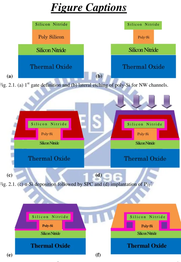
33 Fig. 2.1. (a) 1st gate definition. (b) Lateral etching of poly-Si for NW channels. (c) α-Si
deposition followed by SPC. (d) Implantation of P31 +
. (e) Drive-In at 900oC for 30 min. (f) S/D, NW channels definition and n+ poly-Si for 2nd gate……..…... Fig. 2.2. (a) Layout and (b) cross-sectional view of the double-gated device. ……….. 34 Fig. 2.3. TEM image of a fabricated IDG J-less NW device. ……… 34 Fig. 2.4. Settings of the operation modes……….……...... 35
Chapter 3
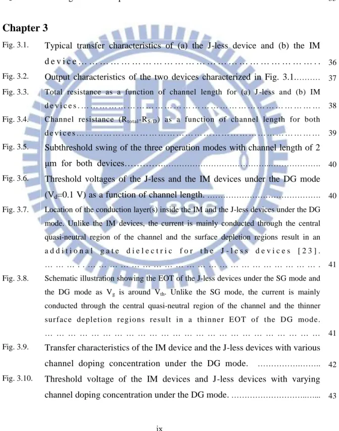
Fig. 3.1. Typical transfer characteristics of (a) the J-less device and (b) the IM
d e v i c e … … … . . 36
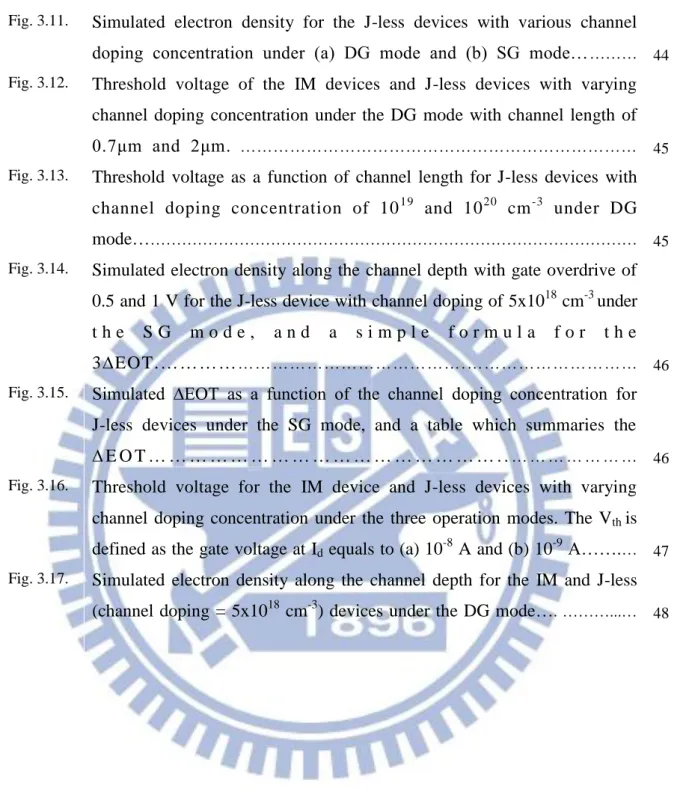
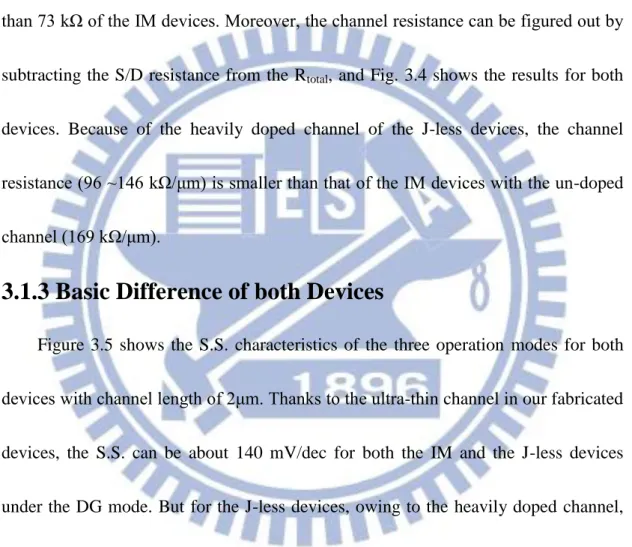
Fig. 3.2. Output characteristics of the two devices characterized in Fig. 3.1.……… 37 Fig. 3.3. Total resistance as a function of channel length for (a) J -less and (b) IM
d e v i c e s . … … … 38 Fig. 3.4. Channel resistance (Rtotal-RS/D) as a function of channel length for both
d e v i c e s … … … 39 Fig. 3.5. Subthreshold swing of the three operation modes with channel length of 2
μm for both devices………….………..………. 40
Fig. 3.6. Threshold voltages of the J-less and the IM devices under the DG mode
(Vd=0.1 V) as a function of channel length. ………. 40
Fig. 3.7. Location of the conduction layer(s) inside the IM and the J-less devices under the DG mode. Unlike the IM devices, the current is mainly conducted through the central quasi-neutral region of the channel and the surface depletion regions result in an a d d i t i o n a l g a t e d i e l e c t r i c f o r t h e J - l e s s d e v i c e s [ 2 3 ] . … … … . . … … … . 41 Fig. 3.8. Schematic illustration showing the EOT of the J-less devices under the SG mode and
the DG mode as Vg is around Vth. Unlike the SG mode, the current is mainly
conducted through the central quasi-neutral region of the channel and the thinner surface depletion regions result in a thinner EOT of the DG mod e. … … … 41 Fig. 3.9. Transfer characteristics of the IM device and the J-less devices with various
channel doping concentration under the DG mode. ……….…….. 42
Fig. 3.10. Threshold voltage of the IM devices and J-less devices with varying
x
Fig. 3.11. Simulated electron density for the J-less devices with various channel
doping concentration under (a) DG mode and (b) SG mode………… 44
Fig. 3.12. Threshold voltage of the IM devices and J-less devices with varying channel doping concentration under the DG mode with channel length of
0.7μm and 2μm. ……… 45
Fig. 3.13. Threshold voltage as a function of channel length for J-less devices with
channel doping concentration of 1019 and 1020 cm-3 under DG
mode……… 45
Fig. 3.14. Simulated electron density along the channel depth with gate overdrive of
0.5 and 1 V for the J-less device with channel doping of 5x1018 cm-3 under
t h e S G m o d e , a n d a s i m p l e f o r m u l a f o r t h e
3∆EOT.……….……… 46
Fig. 3.15. Simulated ∆EOT as a function of the channel doping concentration for
J-less devices under the SG mode, and a table which summaries the
∆ E O T … … … . .… … … 46
Fig. 3.16. Threshold voltage for the IM device and J-less devices with varying
channel doping concentration under the three operation modes. The Vth is
defined as the gate voltage at Id equals to (a) 10-8 A and (b) 10-9 A…….… 47
Fig. 3.17. Simulated electron density along the channel depth for the IM and J-less
1
Chapter 1
Introduction
1.1 Overview
of
Junctionless
Nanowire
Transistors
Nowadays, trends in the microelectronics industry require the structure of smaller and smaller components, and that’s one of the reasons why the field of nanotechnology has been vastly explored and investigated. Over the past decades, the
size of metal-oxide-semiconductor field-effect transistors (MOSFETs) has continually
been shrunk, with the effective channel length now reaching the nano-scale era.
Essentially all the mainstream transistors in mass production are based on the
formation of junctions, and a typical MOS transistor contains two PN junctions to
form the source and drain (S/D), respectively, and in-between the two junctions the
active channel is defined. However, non-planar inversion-mode (IM) devices like
FinFETs encounter difficulties in achieving shallow as well as uniform S/D doping by
using ion implantation on account of shadowing effects caused by the tightened
2
budget and needs the development of costly annealing techniques. That’s one of the
reasons why recently lots of attentions have been paid to the junctionless (J-less)
devices, which feature heavy and homogeneous doping concentration across the S/D
and the channel. In other words, for the J-less devices, the doping concentration in the
channel is almost on the same order as those in the S/D [2]. Because the gradient of
the doping concentration between the S/D and the channel is close to zero, negligible
diffusion takes place, which can eliminate the need for costly ultrafast annealing
techniques [3]-[5]. Additional significant features of the J-less devices include
reduction of the degradation of mobility from surface scattering and outstanding
performance for RF application.
The concept of the J-less multigated transistors has been demonstrated by J. P.
Colinge et al. in 2009 [2]. For the J-less devices, the operation mechanisms is quite
different from that of conventional IM devices considering the heavy and
homogenous doping concentration through the S /D and the channel [6]-[7]. The
J-less devices can effectively reduce the scattering events occurring at the interface
between the gate insulator and the channel since most of the carriers are away from
the interface [8]. It is contrary to the classical IM devices, and is also conducive to
promoting the field-effect mobility of J-less devices. To fabricate a functional J-less
3
allow full depletion of carriers in the channel by the gate so the device can be
effectively turned off. On the other hand, the semiconductor also needs to be heavily
doped to achieve a high on-current. It is essential to consider the above constraints
when designing and fabricating the J-less devices [9].
1.2 Overview of Memory Devices
Over the past two decades, due to the constant reduction in cost and increase in
memory density, the market of memory devices has been growing aggressively. Of all
the memory devices, non-volatile semiconductor memory (NVSM) is indispensable
for portable electronic products since it can retain stored data even if the power is
switched off. From 1967 to 2012, the NVSM has emerged from a floating-gate
concept to the prime technology driver of the electronics industry all around the world.
The floating-gate NVSM was invented by D. Kahng and S. M. Sze in 1967 [10]. And
one of the most important inventions in NVSMs is Flash memory, which possesses
many advantages such as non-volatile, high density, good durability and low power
consumption. However, great obstacles like short-channel effects (SCEs) and
decreased number of stored charges are lying ahead and speculatively scaling of
planar NAND flash technology would stop at around the 10 nm node [11].
4
this device manufacturable with very low thermal budget. Nowadays, several kinds of
J-less Flash memory devices with well-behaved memory characteristics have been
investigated because they possess abundant advantages such as programming/erasing
efficiency, endurance, data retention, and program disturb properties [12]-[13]. In
terms of NAND Flash memory application, one unique and significant advantage of
J-less NW transistors is the superior low series resistance due to the heavy and
homogenous doping concentration through the S/D and the channel. Moreover, a
novel 2-level stacked J-less gate-all-around (GAA) SONOS memory fabricated on
vertical-SiNW platform has been proposed recently [14]. Without forming junctions
on vertical-wires, the stacking process complexity/cost is greatly reduced with
promise towards density improvement. Therefore, the stackable vertical-SiNW J-less
SONOS with high performance is considered as a promising candidate for future
ultra-high density application.
Moreover, the J-less transistors are also suitable to be applied to DRAM
technology. Recently, DARM cells with size down to nanometer level face several
problems, including SCEs, complex process of the storage capacitors, and junction
formation, etc. It is demonstrated that the 1-T DRAM using floating-body effects has
been introduced to vanquish the problem of capacitor formation and can reduce both
5
multiple-gated (MuG) MOSFET becomes an ideal choice for 1T-DRAM with many
advantages such as very low leakage current and a low turn-on voltage due to the lack
of PN junctions [16].
1.3 Motivation
As the devices are scaled down to such an aggressive nanometer regime,
multi-gated field-effect transistors (MuGFETs) are one of the most promising
candidates for future CMOS technologies due to their improved SCEs. Because of the
adoption of the multi-gated configuration, better controllability of channel potential
and a larger driving current can be acquires as compared to classical planar
technologies [17]. In the MuGFETs, NW channels are often employed. An NW is
defined as a stripe-shaped material with a diameter or feature size smaller than 100
nm. NWs can achieve a very large surface-to-volume ratio considering their tiny size
and thus their electrical properties are very sensitive to the surface condition, one of
the reasons for the sprouting research activities conducting on the applications of
NW-based devices in recent years [18].
In order to efficiently shut down the off-state leakage current conducting through
the heavily doped channel in the J-less transistors, the adoption of a MuG
6
previously introduced an independent double-gate (IDG) poly-Si NW transistor with
rectangular-shaped and thin (~ 20 nm) NW channels [19]. Such an IDG scheme
provides more flexibility in device operation by the aid of the two independently
controllable gates, and also has indeed demonstrated the features of high on/off
current ratio and low sub-threshold swing (S.S.) [20].
In this study, we fabricated, measured, and analyzed N-type J-less IDG NW
devices with high doping concentration in the channel. A brief comparison in
conduction mechanisms between the devices with conventional ones with undoped
channels is also made in this work.
1.4 Thesis Organization
In Chapter 2, we present the fabrication of the N-type J-less IDG NW devices by
briefly illustrating and describing the basic process flow. The measurement setups are
also presented in this chapter.
In Chapter 3, we present and discuss the electrical characteristics of the
fabricated devices, which include the on-current, S.S., Vth (threshold voltage) and
SCEs. The results of the two single-gated (SG) modes and the double-gated (DG)
mode are discussed respectively. Also, we compare the electrical characteristics with
7
Finally, we summarize the major findings and conclusions from our
8
Chapter 2
Device Fabrication and Measurement
Setup
2.1 Device Fabrication and Process Flow
Figures 2.1((a) ~ (f)) show the process flow of the device fabrication. Figure 2.2(a)
presents a top view of the completed device, and the schematic illustrations in Fig.
2.1(a) ~ (f) correspond to the cross-sectional images after each step along the cutline
a-b in Fig. 2.2(a).
The fabrication started on Si wafers capped with a 1000 nm-thick thermal oxide.
First, a stack consisted of SiN (60 nm)/ in-situ doped n+ poly-Si (100 nm)/SiN (50
nm) was deposited. After an anisotropic patterning of top SiN/ poly-Si (Fig. 2.1(a)), a
chemical plasma etching with high selectivity to SiN was used for lateral etching of
the poly-Si (Fig. 2.1(b)) to form nanometer-level cavities at the two sides of the stack.
Note that the remaining n+ poly-Si serves the role as the first gate of the completed
device. Then a 15-nm-thick TEOS oxide and a 100-nm-thick amorphous-Si (a-Si)
were deposited to fill the nanometer-level cavities. The a-Si was subsequently
9
2.1(c)). Subsequently an implant using P31+ at the doses of 5 × 1013 cm-2 ~1 × 10¹⁵
cm-2 (Fig. 2.1(d)) was performed, and then the samples were annealed in nitrogen
ambient at 900oC for 30 minutes for driving the dopants into the NW channels (Fig.
2.1(e)).
To reduce S/D resistances, an additional S/D doping was performed by
implanting P31+ at a dose of 5 × 1015 cm-2. Then we defined the channel and S/D
regions by reactive plasma etching, and the materials for forming the 2nd gate
structure including a 15-nm-thick TEOS oxide and a 100-nm-thick in-situ doped n+
poly-Si were deposited as the following step. The n+ poly-Si was subsequently
patterned to serve as the 2nd gate electrode (Fig. 2.1(f)). The device was completed
after standard metallization steps. For the purpose of comparison, inversion mode (IM)
devices with undoped channels were also fabricated with the same process flow for
J-less devices except that the channel doping (Fig. 2.1(d)) was omitted.
2.2 Images of Fabricated Devices
The layout of the IDG device is shown in Fig. 2.2(a). Fig. 2.2(b) shows the
cross-sectional view of the completed device along cutline ( ) in Fig. 2.2(a), with the
channel width and thickness as specified. It can be seen that the 1st gate is surrounded
10
During the fabrication, the formation of nanometer-level cavities using plasma
lateral etching shown in Fig. 2.1(b) is critical to the final nanowire channels, it is
therefore mandatory to check the shape and dimension of the fabricated NW channels
to observe the actual geometry of those cavities. The cross-sectional transmission
electron microscope (TEM) image for a fabricated independent double-gate device is
shown in Fig. 2.3, from which a rectangular NW channel can be observed, and the
thickness is about 16 nm.
In our study, considering that the texture and grain size of the fabricated NW
channels might possess some physical differences if different thermal budget
associated with the process steps was exerted, the same drive-in steps for driving the
dopants into the NW channels were preformed for both devices, either with additional
channel implant or not. Different splits of devices with the same thermal budget help
us compare their transfer characteristics objectively. The electrical characteristics of
the fabricated devices including both J-less and the IM devices are presented and
discussed in Chapter 3.
2.3 Measurement Setup
Electrical transfer characteristics of the fabricated devices reported in this thesis
11
contained in an automated measurement set up, and the equipment integrated in the
system is controlled by the interactive characterization software (ICS) program. In
addition, the measurement temperature was maintained at room temperature of about
25oC.
In our experiment, threshold voltage (Vth) was defined as the value of Vg when Id
was equal to under Vd of 0.1V, where W and L are the channel width and
the channel length, respectively. For the channel width W, the value was estimated
from the TEM images shown in Fig. 2.3. Also the subthreshold swing (S.S.) was
calculated by the following equation:
, (Eq. 2-1)
and for both the J-less and IM devices, the average value in the subthreshold swing is
extracted. Drain induced barrier lowering (DIBL) occurs in a short-channel IM device
that the barrier along the channel for the carriers from the source to surmount is
obviously modulated by the drain bias. In our study, the DIBL is defined as the
difference in Vth when the drain voltage is increased from 0.1 V to 1.0 V
(DIBL=Vth(Vd=0.1 V)-Vth(Vd=1 V)). It should be noted that the meaning of the
“DIBL” parameters measured with the above scheme need to be carefully addressed in the J-less devices considering the difference in operation principles as compared
12
Settings of the operation modes are listed in Fig. 2.4. SG-1 and SG-2 modes
denote the scheme when either the 1st or 2nd gate, respectively, serves as the driving
gate while the other gate electrode is grounded. In DG mode, both gates are connected
13
Chapter 3
Results and Discussion
3.1 Basic Electrical Characteristics
3.1.1 Transfer Curves
Figures 3.1(a) and 3.1(b) show the transfer curves of the J-less and IM devices,
respectively. In Fig. 3.1(b), due to the existence of un-gated regions in the operation
of SG-1 mode [21], the electrical performance of the SG-1 mode for the IM device is
basically worse than that of the SG-2 mode. This issue is efficiently ameliorated when
adopting the J-less scheme as shown in Fig. 3.1(a). This is because the high doping
concentration in the channel of the J-less device tends to eliminate the impacts of the
un-gated regions stated above. In Fig. 3.1, moreover, the J-less transistor displays
more negative Vth values as compared with the IM one, owing to the adoption of the
same doping type with the S/D and the heavily doped channels (channel doping is
estimated to be around 1x1020 cm-3). In addition, because of the ultra-thin channel
(see Fig. 2.3), the J-less device can still be effectively turned off in all operation
modes despite the very high doping concentration contained in the channel. The
14
With the two types of devices, it should be noted that there are some differences
in the conduction mechanisms. For the IM devices, the current mainly conducts
through the inversion layer formed near the interface between the channel and the
gate dielectric. However, it can be observed that the curves of the J-less devices
conspicuously shift to the left side (with more negative value of Vth), showing the
normally-on characteristics in Fig. 3.1(a). Unlike conventional IM devices that the on
current conduction is mainly restricted in the inversion layer close to the
channel/oxide interface, in J-less devices the major conduction is through the
quasi-neutral region inside the channel. For our fabricated N-type J-less devices, if the
gate bias is not sufficiently negative to effectively deplete the free carriers in the
ultra-thin channel, a high leakage current conducting through the inner quasi-neutral
region will remain. In this regard, DG mode [22] is more efficient since it depletes the
channel from the two sides. When it comes to gate coupling effect, as long as the
channel fin thickness is sufficiently thin, the device can be turned off effectively with
the adoption of DG configuration, even though the channel is heavily doped. For the
IM devices, the DG mode can strongly improve the gate controllability to form the
inversion layer and hence turn the devices on more effectively, and also enhance the
electrical performance obviously. For the J-less devices, the DG mode can use the two
15
effectively, leading to a smaller S.S. and a larger Vth than those in the SG modes.
In Figs. 3.1(a) and 3.1(b) we can also compare the S.S. characteristics under
three operation modes for the two types of devices. For the IM devices, the SG-1
mode shows the worst S.S. among the three modes. This is because of the existence of
un-gated regions as operated under the SG-1 mode as mentioned before. Nevertheless,
for the J-less devices, the high doping concentration in the channel tends to reduce the
impacts from the un-gated regions stated above. Therefore, the gate controllability of
the SG-1 mode is improved for the J-less devices, which is less affected by the
un-gated regions. Ion of the SG-1 mode is also obviously improved and becomes
comparable to those of the other two modes.
3.1.2 Output Characteristics
Figure 3.2 shows the significant performance enhancement made by the J-less
device over the IM one. For the J-less devices, the on-state current conduction occurs
essentially through the whole channel layer rather than the regions close to the
channel surface as the IM devices do [22]. As can be seen in the figure, the J-less
device can provide about 333% enhancement of saturation current at Vg-Vth = 3 V and
Vd =5 V over the IM one.
When it comes to the S/D resistance, it can be extracted from the Id-Vd curves of
16
the total resistance ( ) as a function of the channel length of both devices.
Here we can extract the S/D resistance from the intercept of the y-axis of the plots.
Owing to the extra implantation which can reduce the S/D resistance of the J-less
devices, the S/D resistance of the J-less devices is about 69 kΩ, just a little smaller than 73 kΩ of the IM devices. Moreover, the channel resistance can be figured out by
subtracting the S/D resistance from the Rtotal, and Fig. 3.4 shows the results for both
devices. Because of the heavily doped channel of the J-less devices, the channel resistance (96 ~146 kΩ/μm) is smaller than that of the IM devices with the un-doped channel (169 kΩ/μm).
3.1.3 Basic Difference of both Devices
Figure 3.5 shows the S.S. characteristics of the three operation modes for both devices with channel length of 2μm. Thanks to the ultra-thin channel in our fabricated devices, the S.S. can be about 140 mV/dec for both the IM and the J-less devices
under the DG mode. But for the J-less devices, owing to the heavily doped channel,
the S.S. under the SG-1 mode and SG-2 mode is worse than that under the DG mode.
It is interesting to see that, if we compare the S.S. under the SG-2 mode of the J-less
devices with that of the IM devices, the S.S. under the SG-2 mode of the J-less
devices are much more worse than that of the IM devices. This indicates the present
17
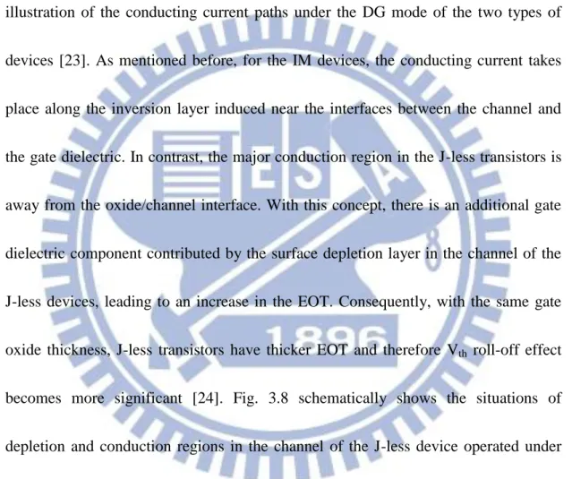
Figure 3.6 compares the Vth roll-off effect of the fabricated J-less and IM devices.
It can be seen that the J-less transistors perform worse than the IM counterparts. Such
a phenomenon can be expounded from the concept of the difference in the effective
oxide thickness (EOT) between the two types of devices. Fig. 3.7 is the schematic
illustration of the conducting current paths under the DG mode of the two types of
devices [23]. As mentioned before, for the IM devices, the conducting current takes
place along the inversion layer induced near the interfaces between the channel and
the gate dielectric. In contrast, the major conduction region in the J-less transistors is
away from the oxide/channel interface. With this concept, there is an additional gate
dielectric component contributed by the surface depletion layer in the channel of the
J-less devices, leading to an increase in the EOT. Consequently, with the same gate
oxide thickness, J-less transistors have thicker EOT and therefore Vth roll-off effect
becomes more significant [24]. Fig. 3.8 schematically shows the situations of
depletion and conduction regions in the channel of the J-less device operated under
SG or SG mode at Vg ~Vth. Since Vth is determined with the constant current scheme,
thickness of the conduction (quasi-neural) region for the two modes should be
comparable. Thus for the SG mode it needs a thicker depletion region (at the
driving-gate side) than the DG modes to achieve the same current conduction at Vg
18
controllability under the SG mode owing to the thicker EOT, resulting in the more
negative Vth over that of the DG mode (Fig. 3.1). The thinner EOT for the DG mode
also explains the S.S. improvement with the DG mode of operation shown in Fig. 3.5.
3.2 Electrical Characteristics
3.2.1 Gate Controllability
Figure 3.9 shows the transfer curves of the IM device and the J-less devices with
various channel doping concentration under the DG mode with channel length of 0.7
μm. It should be noticed that the Vth of the J-less devices becomes more negative as
the channel doping concentration increases. Such a phenomenon indicates that the
higher channel doping concentration the J-less devices have, the harder the J-less
devices can be effectively turned off at Vg = 0. In other words, for the J-less devices, a
more negative gate bias is necessary to deplete the channel and shut off the off-state
leakage current with the increasing channel doping concentration. Moreover, for the
J-less devices with higher channel doping concentration, the On/Off current ratio can
still reach 106~107 which is comparable to that of the IM devices (Off current here is
defined as the minimum of the drain current).
Figure 3.10 shows the Vth characteristics as a function of channel doping
19
specific condition were measured from 10 devices with channel length of 0.4 μm. As
mentioned above, the Vth characteristics become more and more negative as the
channel doping concentration of the J-less devices increases. Moreover, the Vth
fluctuation also gets much larger with the increasing channel doping concentration, in
contrast to the results the IM devices exhibit. This is because the conduction
mechanisms for the J-less devices are distinctly different from those of the IM ones.
For the J-less scheme, the carriers are mainly concentrated in the channel center while
the channel surface is depleted [23]. The channel depletion layer would serve as an
extra gate dielectric layer and aggravate the gate controllability and Vth fluctuation.
More details and analysis will be discussed later.
Here we can use the TCAD simulation to analyze the differences in the
conduction mechanisms between the two types of devices. The simulation is based on
the assumption that the structures are with uniform doping concentration throughout
the channel and, for simplicity, the S/D series resistance is ignored for the J-less
devices [23]. The channel doping element is phosphorous at carrier concentrations of
5×1018 cm-3, 8×1018 cm-3, and 1×1019 cm-3. The channel thickness is 16 nm while the
gate oxide thickness is 15 nm. Moreover, the work-function of the gate electrode is
assumed to be 4.17 eV, and here we ignore the quantum effects in order to simplify
20
nA. Figs. 3.11(a) and (b) show the simulation results of the electron density along the
channel depth for the J-less devices with various channel doping concentration under
the DG and SG modes, respectively. As the gate overdrive equals 1 V, Fig. 3.11(a)
exhibits that the active electrons are concentrated in the central Si channel, and the
carrier concentration is more tightly distributed with the increasing channel doping
concentration. It means that with a higher channel doping concentration, the J-less
devices can offer more carriers at the same gate overdrive.
As mentioned before, the J-less devices exhibit the unique conduction
mechanism with conducting current flowing mainly through the channel body rather
than at the oxide/silicon interface, which is in strong contrast to that of the IM devices.
Moreover, Figs. 3.11(a) and (b) show distinct differences between the DG mode and
the SG one. In Fig. 3.11(b), it can be noticed that the peak of carrier density is moving
toward the interface with decreasing channel doping concentration under the same
gate overdrive. This is reasonable since under the DG mode the channel is depleted
from the two opposite sides of the channel and the side depletion regions tend to
widen and approach the channel center as the device is turned off, while under the SG
mode the depletion region is modulated by the driving gate bias from only one side of
the channel, resulting in the asymmetrical carrier distribution. For the SG mode with
21
significant.
The Vth as a function of channel doping concentration under the DG mode is
given in Fig. 3.12 for devices with channel length of 2 and 0.7 μm. It can be seen that,
with channel length shortened from 2 to 0.7 μm, Vth drop is more significant for the
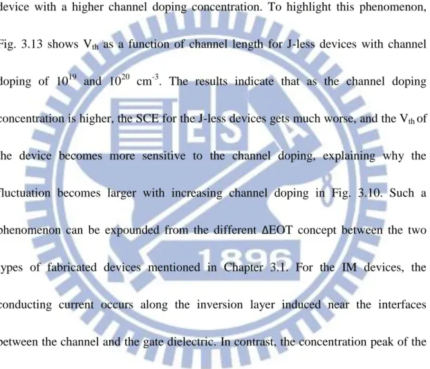
device with a higher channel doping concentration. To highlight this phenomenon,
Fig. 3.13 shows Vth as a function of channel length for J-less devices with channel
doping of 1019 and 1020 cm-3. The results indicate that as the channel doping
concentration is higher, the SCE for the J-less devices gets much worse, and the Vth of
the device becomes more sensitive to the channel doping, explaining why the
fluctuation becomes larger with increasing channel doping in Fig. 3.10. Such a
phenomenon can be expounded from the different ∆EOT concept between the two
types of fabricated devices mentioned in Chapter 3.1. For the IM devices, the
conducting current occurs along the inversion layer induced near the interfaces
between the channel and the gate dielectric. In contrast, the concentration peak of the
conduction carriers of J-less transistors is away from the interface and is located at the
center of the Si channel, as shown in Fig. 3.11(a). In this figure the electron density is
simulated as a function of Si channel depth with different channel doping
concentrations under the gate overdrive of 1 V under DG mode. The simulated
22
3.11(b) in which we can see that the peak carrier concentration varies with channel
doping concentration. Here, for simplicity, we define the extra EOT contributed by
the Si depletion layer as the average location of the electrons with respect to the Si
channel surface of the driving gate side, and can be calculated with the formula:
,
(Eq. 3.1)where Ne(x) is the number of active electrons as a function of location and x is the
location of the electrons with respect to the Si channel surface. Following the formula,
we can quantitatively acquire the contribution of the Si depletion layer to the EOT
which is related to the channel doping concentration, as shown in Fig. 3.11(b).
Fig. 3.14 shows the electron density as a function of depth of Si channel with the
channel doping concentration equaling 5×10¹⁸ (cm-3) under the SG mode with gate
overdrive of 1 and 0.5 V. In this picture, we can observe that not only the height of
peak of the carrier density but also its location depend on the gate overdrive condition
as operated under SG mode. Here we define the displacement of the peak of the
carrier density with gate overdrive varies from 1V to 0.5 V as ∆EOT, i.e.,
23
By the way, because of the differences of dielectric constant between the Si and SiO2,
the EOT is equal to one-third of the thickness of Si (or TSi 3EOT ). And in Fig.
3.16, we also take the consideration mentioned above into account.
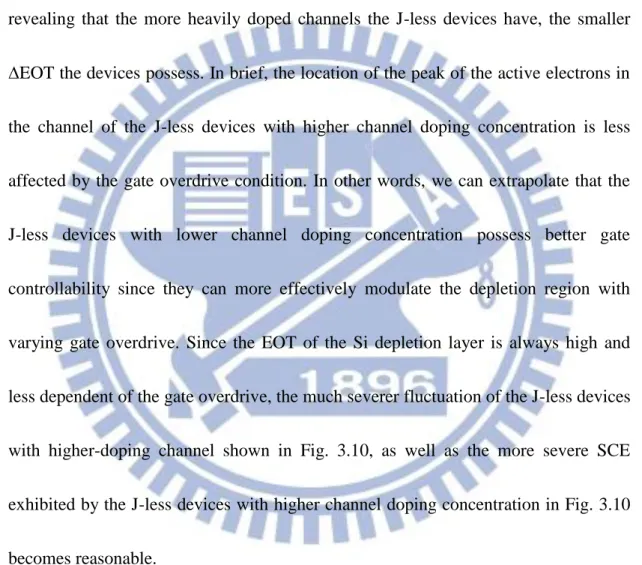
Fig. 3.15 demonstrates the ∆EOT as a function of channel doping concentration,
revealing that the more heavily doped channels the J-less devices have, the smaller
∆EOT the devices possess. In brief, the location of the peak of the active electrons in
the channel of the J-less devices with higher channel doping concentration is less
affected by the gate overdrive condition. In other words, we can extrapolate that the
J-less devices with lower channel doping concentration possess better gate
controllability since they can more effectively modulate the depletion region with
varying gate overdrive. Since the EOT of the Si depletion layer is always high and
less dependent of the gate overdrive, the much severer fluctuation of the J-less devices
with higher-doping channel shown in Fig. 3.10, as well as the more severe SCE
exhibited by the J-less devices with higher channel doping concentration in Fig. 3.10
becomes reasonable.
3.2.2 Variation of Different Channel Doping Concentration
Figures 3.16(a) and (b) show the Vth as a function of channel doping
24
of 2 μm. In Fig. 3.16(a) the magnitude of the current used to determine Vth is 10-8 A,
and changed to 10-9 A in Fig. 3.16(b). Obviously the definition of Vth would affect the
results, but generally the trends observed in the two figures are similar. That is, the
Vth of DG mode for the IM device is the smallest among the three modes but
gradually the differences in Vth value among different modes become smaller as the
doping concentration increases and eventually the Vth of DG mode becomes the
largest as the channel doping is sufficiently large. Occurrence of the crossing point
depends on the criterion for judging the Vth, indicting the impact of the artificial
definition of Vth. As mentioned in Chapter 3.1, due to the unique conduction
mechanism of the J-less devices, the conducting current flow mainly through the
channel body rather than at the oxide/silicon interface. Also, utilizing the DG
structure for the J-less devices allows the simultaneous use of the two gates to deplete
the channel and therefore turn the devices off more effectively, leading to a larger Vth
than those in the SG modes. On the other hand, for the IM devices the operation
depends on the formation of an inversion layer by the applied gate bias, rather than
the depletion of the channel.
According to [25], the author claimed that the driving current of the J-less
devices with higher doping concentration (>1019 cm-3) is almost contributed by the
25
dominated by the bulk current but still partially affected by the current formed near
the interface between the channel and the gate dielectric. However, unlike the IM and
accumulation-mode devices which rely on an inversion or accumulation layer induced
at the channel surface for conduction, the on-state current conduction of the J-less
devices occurs essentially through the whole channel.
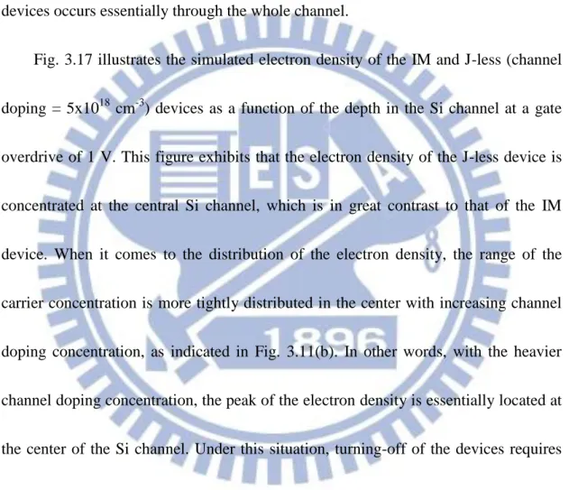
Fig. 3.17 illustrates the simulated electron density of the IM and J-less (channel
doping = 5x1018 cm-3) devices as a function of the depth in the Si channel at a gate
overdrive of 1 V. This figure exhibits that the electron density of the J-less device is
concentrated at the central Si channel, which is in great contrast to that of the IM
device. When it comes to the distribution of the electron density, the range of the
carrier concentration is more tightly distributed in the center with increasing channel
doping concentration, as indicated in Fig. 3.11(b). In other words, with the heavier
channel doping concentration, the peak of the electron density is essentially located at
the center of the Si channel. Under this situation, turning-off of the devices requires
an ultra-thin channel so that the channel can be effectively depleted. As mentioned
before, the gate controllability is worse for the SG mode as compared with that of the
DG mode, especially for the SG-1 mode. Therefore, as the channel doping is
sufficiently high, the J-less devices show Vth characteristics (DG > SG-2 >SG-1)
26
Chapter 4
Conclusion
In this work, we have successfully fabricated and characterized a novel n-type
J-less poly-Si NW transistors featuring an independent double-gated configuration.
Because of the ultra-thin channel (about 16 nm), the J-less device can be effectively
turned off in all operation modes despite the very high doping concentration contained
in the channel. Moreover, as compared with the IM counterparts, some intriguing
characteristics are revealed. For the IM devices, the current mainly conducts through
the inversion layer formed near the interface between the channel and the gate
dielectric. However, unlike the conventional IM devices that the on current
conduction is mainly restricted in the inversion layer close to the channel/oxide
interface, in J-less devices the major conduction is through the quasi-neutral region
inside the channel. Therefore, as the J-less devices are on, the carriers flow mainly
through the whole Si channel, thus the current level is significantly larger than that of
the IM ones. From the TCAD simulation results, distribution of the carriers in the
channel and the operation mechanisms of the two types of devices are analyzed.
27
turned on, the quasi-neutral region of the J-less device gradually expands from the
channel center to the interfaces with increasing gate overdrive. For our fabricated
n-type J-less devices, if the gate bias is not sufficiently negative to effectively deplete
the free carriers in the ultra-thin channel, a high leakage current conducting through
the inner quasi-neutral region will remain. In this regard, DG mode is more efficient
since it depletes the channel from the two sides.
When it comes to the Vth characteristics, due to the additional EOT contributed
by the surface Si depletion region, the J-less devices exhibit worse SCEs than the IM
devices like more severe Vth roll-off. Also, the J-less devices have poorer gate
controllability under the SG mode owing to the thicker EOT, resulting in the more
negative Vth over that of the DG mode. On the other hand, the higher channel doping
concentration the J-less devices have, the harder the J-less devices can be effectively
turned off at Vg = 0. Moreover, as the channel doping concentration is higher, the
SCE for the J-less devices gets much worse, and the Vth of the device becomes more
sensitive to the channel doping. Using the TCAD simulation, we can extrapolate that
the J-less devices with lower channel doping concentration possess better gate
controllability since they can more effectively modulate the depletion region with
varying gate overdrive.
28
J-less device is concentrated at the central Si channel, which is in great contrast to that
of the IM device. In other words, with the heavier channel doping concentration, the
peak of the electron density is essentially located at the center of the Si channel. Thus,
turning-off of the devices requires an ultra-thin channel so that the channel can be
effectively depleted. Finally, as the channel doping is sufficiently high, the J-less
devices show Vth characteristics (DG > SG-2 >SG-1) opposite to those observed for
29
References
[1] D. J. Frank, R. H. Dennard, E. Nowak, P. M. Solomon, Y. Taur, and H.-S. P. Wong, “Device scaling limits of Si MOSFETs and their application dependencies,”
Proc. IEEE, vol. 89, no. 3, pp. 259–288, Mar. 2001.
[2] C.-W. Lee, A. Afzalian, N. D. Akhavan, R. Yan, I. Ferain, and J. P. Colinge, “Junctionless multigate field-effect transistor,” Appl. Phys. Lett., vol. 94, p. 053511, 2009.
[3] A. Kranti, R. Yan, C. W. Lee, I. Ferain, R. Yu, N. D. Akhavan, P. Razavi, and J. P. Colinge, “Junctionless nanowire transistor (JNT): Properties and design guidelines,” Proc. Euro. Solid-State Device Res. Conf. (ESSDERC), 2010, pp. 357–360.
[4] C. Y. Chen, J. T. Lin, M. H. Chiang, and K. Kim, “High-performance ultra-low
power junctionless nanowire FET on SOI substrate in subthreshold logic application,”
Proc. SOI Conf., 2010, pp. 1–2.
[5] J. P. Colinge, C. W. Lee, I. Ferain, N. D. Akhavan, R. Yan, P. Razavi, R. Yu, A. N. Nazarov, and R. T. Doria, “Reduced electric field in junctionless transistors,” Appl.
Phys. Lett., vol. 96, p. 073510, 2009.
30
P. Razavi, B. O’Neill, A. Blake, M. White, A.-M. Kelleher, B. Mc-Carthy, and R. Murphy, “Nanowire transistors without junctions,” Nature Nanotechnol., vol. 5, pp. 225–229, 2010.
[7] C. W. Lee, A. Borne, I. Ferain, A. Afzalian, R. Yan, N. D. Akhavan, P. Razavi, and J. P. Colinge, “High temperature performance of silicon junctionless MOSFETs,”
IEEE Trans. Electron Devices, vol. 53, no. 3, pp. 620–625, Mar. 2010.
[8] E. Gnani, A. Gnudi, S. Reggiani, G. Baccarani, “Physical model of the
Junctionless UTB SOI-FET,” IEEE Trans. Electron Devices, pp.941-948, 2012.
[9] E. Gnani, A. Gnudi, S. Reggiani, G. Baccarani, “Numerical investigation on the
junctionless nanowire FET,” ULIS Int. Conf., 2011.
[10] D. Kahng, S.M. Sze, “A floating gate and its application to memory devices,”
Bell Syst. Tech. J., 46, 1967.
[11] K. Kim, “From the future Si technology perspective: Challenges and opportunities”, IEDM Tech. Dig., pp 1-9, 2010.
[12] H. T. Lue, E. K. Lai, Y. H. Hsiao, S. P. Hong, M. T. Wu, F. H. Hsu, N. Z. Lien,
S. Y. Wang, L. W. Yang, T. Yang, K. C. Chen, K. Y. Hsieh, R. Liu, and C.-Y. Lu, “A
novel junction-free BE-SONOS NAND flash,” VLSI Symp. Tech. Dig., pp. 140-141,
2008.
31
“Nonvolatile memory by all-around-gate junctionless transistor composed of silicon nanowire on bulk substrate,” IEEE Electron Device Lett., vol. 32, no. 5, pp. 1388-1396, 2011.
[14] Y. Sun, H. Y. Yu, N. Singh, K. C. Leong, E. Quek, G. Q. Lo, G, D. L. Kwong, “Demonstration of memory string with stacked junction-less SONOS realized on vertical silicon nanowire,” IEDM Tech. Dig, 9.7.1-9.7.4, 2011.
[15] S. Okhonin, M. Nagoga, J. M. Sallese, P. Fazan, “A capacitor-less SOI
1T-DRAM concept,” Proc. Int. SOI conf., pp. 153-154, 2001.
[16] R. Yan, I. Ferain, A. Kranti, N. D. Akhvan, P. Razavi, R. Yu, J. P. Colinge,
"Nanowire zero-capacitor DRAM transistors with and without junctions,” IEEE
Nanotechnology Conf., pp.242-245, 2010.
[17] E. J. Nowak, R. H. Dennard, P. M. Solomon, A. Bryant, O. H. Dokumaci, A. Kumar, X. Wang, J. B. Johnson, and M. V. Fischetti., “Silicon CMOS devices beyond scaling,” IBM J. Res. Develop., vol. 50, no. 4/5, pp. 339-361, 2006.
[18] E. Gnani, A. Gnudi, S. Reggiani, G. Baccarani, “Theory of the junctionless
nanowire FET,” IEEE Trans. Electron Devices, pp.2903-2910, 2011.
[19] W. C. Chen, H. C. Lin, Y. C. Chang, C. D. Lin and T. Y. Huang, “In situ doped
source/drain for performance enhancement of double-gated poly-Si nanowire transistors,” IEEE Trans. Electron Devices, vol. 57, no. 7, pp.1608-1615, 2010.
32
[20] H. C. Lin, W. C. Chen, C. D. Lin and T. Y. Huang, “Performance enhancement
in double-gated poly-Si nanowire transistors with reduced nanowire channel
thickness,” IEEE Electron Device Lett., vol. 30, no. 6, pp. 644-646, 2009.
[21] W. C. Chen, C. D. Lin, H. C. Lin and T. Y. Huang, “A novel double-gated nanowire TFT and investigation of its size dependency,” VLSI-TSA. Int. Symp., pp. 121-122, 2009.
[22] W. Chaisantikulwat, M. Mouis, G. Ghibaudo, S. Cristoloveanu, J.Widiez, M. Vinet, and S. Deleonibus, “Experimental evidence of mobility enhancement in short-channel ultra-thin body double-gate MOSFETs by magnetoresistance technique,” Solid State Electron., vol. 51, no. 11/12, pp. 1494–1499, Nov./Dec. 2007. [23] J. P. Wu, “Fabrication and Characterization of P-Type Accumulation-Mode Independent Double-Gated Poly-Si Nanowire Transistors”, Master thesis, Institute of
Electronics, National Chiao Tung University, p. 49, Mar. 2011.
[24] J. P. Colinge, C. W. Lee, I. Ferain, N D. Akhavan, R. Yan, P. Razavi, R. Yu, A. N. Nazarov and R. T. Doria, “Reduced electric field in junctionless transistors,” Appl.
Phys. Lett., vol. 96, no. 7, p. 073510, Feb. 2010.
[25] J. P. Colinge, “Junctionless transistors”, Silicon Nanoelectronics Workshop, pp.69-70, June 12-13, 2011.
33 Poly-Si
Thermal Oxide
Silicon Nitride S i l i c o n N i t r i d eFigure Captions
(a) (b)Fig. 2.1. (a) 1st gate definition and (b) lateral etching of poly-Si for NW channels.
(c) (d)
Fig. 2.1. (c) α-Si deposition followed by SPC and (d) implantation of P31+
(e) (f)
Fig. 2.1. (e) Drive-in at 900oC for 30 min and (f) S/D, NW channels definition and n+
poly-Si for 2nd gate.
Thermal Oxide
Silicon Nitride
Poly Silicon S i l ic o n Ni tr id eThermal Oxide
Silicon Nitride
S i l i c o n N i t r i d e Poly-SiThermal Oxide
Silicon Nitride Poly-Si S i l i c o n N i t r i d e S i l i c o n N i t r i d eThermal Oxide
Silicon Nitride Poly-SiThermal Oxide
Silicon Nitride Poly-Si S i l i c o n N i t r i d e34
(a) (b)
Fig. 2.2. (a) Layout and (b) cross-sectional view of the double-gated device.
Fig. 2.3. TEM image of a fabricated IDG J-less NW device.
Channel Length b a 1st Gate 2nd Gate Source Gate Drain Gate 1st Gate
Thermal Oxide
Silicon Nitride S i l i c o n N i t r i d e Channel Thickness 1st Gate Oxide Channel Width 2nd Gate Oxide 2nd Gate35
36 Vg (V) -3 -2 -1 0 1 2 3 4 I d ( A) 10-15 10-14 10-13 10-12 10-11 10-10 10-9 10-8 10-7 10-6 DG Mode SG-1 Mode SG-2 Mode IM Device Lc=2m Vd=0.1 V Tox=15 nm
Fig. 3.1. Typical transfer characteristics of (a) the J-less device and (b) the IM device.
(a) (b) Vg (V) -3 -2 -1 0 1 2 3 4 5 I d ( A) 10-15 10-14 10-13 10-12 10-11 10-10 10-9 10-8 10-7 10-6 DG Mode SG-1 Mode SG-2 Mode J-less device (Nc=1E20 cm-3) Lc=2m Vd=0.1 V Tox=15 nm
37 Drain Voltage (V) 0 1 2 3 4 5 Drive Current (A) 0 1x10⁻⁶ 2x10⁻⁶ 3x10⁻⁶ 4x10⁻⁶ 5x10⁻⁶ J-less device IM Device V g-Vth=0~3 V Step=1 V L c=2 m DG Mode
~333%
38
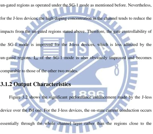
Fig. 3.3 Total resistance as a function of channel length for (a) J-less and (b) IM devices.
Channel Length(
m)
0.0 0.5 1.0 1.5 2.0 2.5Tot
al Resis
tan
ce(
M
)
0.0 0.1 0.2 0.3 0.4 0.5 0.6 0.7 Vd=0.2 V Vd=0.3 V Vd=0.4 V J-less Devices(Channel doping =1E20cm-3)
Vg-Vth=3 V DG Mode RS/D ~ 15 k
Channel Length(
m)
0.0 0.5 1.0 1.5 2.0 2.5Tot
al Resis
tan
ce(
M
)
0.0 0.2 0.4 0.6 0.8 Vd=0.2 V Vd=0.3 V Vd=0.4 V IM Devices Vg-Vth=3 V DG Mode RS/D ~ 25 k39
Fig. 3.4 Channel resistance (Rtotal-RS/D) as a function of channel length for both devices.
Channel Length(m)
0.0 0.5 1.0 1.5 2.0 2.5Chan
nel Res
ista
nce
(M
)
0.0 0.2 0.4 0.6 0.8 Vd=0.2 V Vd=0.3 V Vd=0.4 V J-less Devices Vg-Vth=3 V DG Mode Channel doping =1E20 (cm-3) IM Devices40
IM device J-less device
Subthr
eshol
d Sw
ing
(m
V/dec
)
100 150 200 250 300 350 400 450 500 DG Mode SG-2 Mode SG-1 Mode Vd=0.1 V Tox=15 nm Lchannel= 2 m Channel Length(m) 0.2 0.4 0.6 0.8 1.0 1.2 1.4 1.6 1.8 2.0 2.2 V th (V ) -2.0 -1.5 -1.0 -0.5 0.0 0.5 1.0 1.5 2.0 J-less Device IM Device Vd=0.1 V Tox=15 nm DG ModeFig. 3.6 Threshold voltages of the J-less and the IM devices under the DG mode
(Vd=0.1 V) as a function of channel length.
S.S. IM device J-less device
DG 139(mV/dec) 140(mV/dec)
SG-1 451(mV/dec) 473(mV/dec)
SG-2 198(mV/dec) 437(mV/dec)
Fig. 3.5 Subthreshold swing of the three operation modes with channel length of 2 μm for both devices.
41
Fig. 3.7 Location of the conduction layer(s) inside the IM and the J-less devices under the DG mode. Unlike the IM devices, the current is mainly conducted through the central quasi-neutral region of the channel and the surface depletion regions result in an additional gate dielectric for the J-less devices [23].
<IM device>
<J-less device>
D
S
D
Gate
Gate
Depletion LayerConduction region
Toxe
S
Gate
Gate
Conduction regionToxe
Conduction region
S
D
Gate
Gate
Depletion LayerToxe Conduction region
D
S
Gate
Gate
ToxeFig. 3.8 Schematic illustration showing the EOT of the J-less devices under the SG mode
and the DG mode as Vg is around Vth. Unlike the SG mode, the current is mainly
conducted through the central quasi-neutral region of the channel and the thinner surface depletion regions result in a thinner EOT of the DG mode.
42
Vg (V)
-2 -1 0 1 2I
d(A
)
10-15 10-14 10-13 10-12 10-11 10-10 10-9 10-8 10-7 10-6 10-5 Nc=1e20 (cm-3) Nc=7e19 (cm-3) Nc=4e19 (cm-3) Nc=1e19 (cm-3) Nc=5e18 (cm-3) IM DeviceVd=0.1 V, Tox=15 nm
DG Mode
Lc=0.7
m
Fig. 3.9 Transfer characteristics of the IM device and the J-less devices with various channel doping concentration under the DG mode.
43
Channel Doping Concentration (cm
-3)
IM 5e+18 1e+19 4e+19 1e+20
V
th(V)
-1.5 -1.0 -0.5 0.0 0.5 1.0 1.5Vd=0.1 V, Lc=0.4
m
Tox=15 nm
DG Mode
Fig. 3.10 Threshold voltage of the IM devices and J-less devices with varying channel doping concentration under the DG mode.