國 立 交 通 大 學
電子工程學系 電子研究所碩士班
碩 士 論 文
金屬誘發側向結晶複晶矽 P 型多晶矽薄膜電晶體
的元件特性及熱載子效應研究
A Study on Device Characteristics and Hot-Carrier
Effects of P-Channel Metal-Induced-Lateral Crystallized
Poly-Si Thin-Film Transistors
研 究 生: 林庭輔
指導教授: 黃調元 博士
林鴻志 博士
金屬誘發側向結晶複晶矽 P 型多晶矽薄膜電晶體
的元件特性及熱載子效應研究
A Study on Device Characteristics and Hot-Carrier
Effects of P-Channel Metal-Induced-Lateral Crystallized
Poly-Si Thin-Film Transistors
研 究 生:林庭輔 Student: Tin-Fu Lin 指導教授:黃調元 博士 Advisors: Dr. Tiao-Yuan Huang
林鴻志 博士 Dr. Horng-Chih Lin
國立交通大學
電子工程學系 電子研究所碩士班
碩士論文
A Thesis
Submitted to Department of Electronics Engineering & Institute of Electronics College of Electrical and Computer Engineering
National Chiao-Tung University in Partial Fulfillment of the Requirements
for the Degree of Master in
Electronic Engineering July 2010
Hsinchu, Taiwan, Republic of China
i
金屬誘發側向結晶複晶矽 P 型多晶矽薄膜電晶體
的元件特性及熱載子效應研究
學生:林庭輔 指導教授:林鴻志博士 黃調元博士 國立交通大學 電子工程系 電子研究所碩士班摘 要
在本篇論文中,我們利用一種新穎的測試結構,來分析 P 型金屬誘發側向結 晶複晶矽薄膜電晶體(MILC-TFT)的通道結晶品質、以及可靠度問題。藉由量測 此獨特電晶體的基本電性,我們便可以了解通道中特定位置的結晶品質對電性的 直接關聯。藉由此結構,我們能夠很容易地分析元件的對稱(SSW)、非對稱引洞 (ASW)等組態、以及通道長度(L)對於基本電性的影響,這些不同的引洞位置、 以及不同的通道長度的組合將可能產生較差的薄膜品質,例如在長通道下(L > 5 μm)將有固相結晶(SPC)晶粒的出現,而在某個通道長度的範圍裡(L = 2~5 μm), 對稱引洞元件的通道中間會產生許多缺陷,這些較差的結晶品質將導致元件特性 變差。 另一方面,有了此特殊結構的幫助,我們便能夠深入解析熱載子造成元件局 部地區的衰退。我們發現當元件操作於在較大的閘極與汲極間的壓降時,更多的 電子將會注入閘極氧化層,進而導致元件更快速的衰退。值得一提的是,這些電ii
性的變化顯示出熱載子將會嚴重的損害 MILC-TFT 閘極氧化層,而導致大量的 電子被閘極氧化層捕捉。這傷害於固相結晶薄膜電晶體(SPC-TFT)比較輕微,然 而 SPC-TFT 的主要衰退則是由通道中額外形成的缺陷所引起,此缺陷是由於通 道裡的弱鍵被熱載子打斷而產生的。
iii
A Study on Device Characteristics and Hot-Carrier
Effects of P-Channel Metal-Induced-Lateral Crystallized
Poly-Si Thin-Film Transistors
Student: Tin-Fu Lin Advisors: Dr. Horng-Chih Lin
Dr. Tiao-Yuan Huang
Department of Electronics Engineering and Institute of Electronics National Chiao Tung University, Hsinchu, Taiwan
ABSTRACT
In this study, we have fabricated a novel test structure to analyze the effects of location-dependent film crystallinity and reliability issues in p-channel MILC TFTs. By using this unique structure, impacts of the film crystallinity on device characteristics can be directly analyzed by the measurement of transfer characteristics on the monitor transistors embedded in the test structure. Moreover, it is convenient to address the impacts of asymmetry seeding window (ASW) and symmetry seeding window (SSW) configurations as well as the channel length (L) on device performance. The generation of inferior film crystallinity in the poly-Si, such as the SPC granular structure or defect rich region, is closely related to the seeding window arrangement and the channel dimensions. The SPC granular structure mainly degrades devices characteristics of ASW devices with L > 5 μm, while the impacts of the existence of defect-rich region on SSW devices are peaked at L = 2~5 μm.
iv
With the help of the novel test transistors, the location-dependent damage can be resolved by measuring the degradation of subthreshold characteristics of monitor transistors. We found that major degradation arises from the electron injection in the gate oxide as drain bias is large and the voltage difference between the gate and drain is significant. It is worth to mention that the MILC devices under hot carrier stress suffer more from the electron trapping in the gate insulator. However, the SPC devices are more vulnerable to the generation of additional trap sites in the channel due to the abundance of weak bonds which are easily struck and broken by energetic carriers.
v
Acknowledgement
碩士生涯即將趨向尾聲,於這短短的兩年裡,首先我將對於我的指導教授表 達深摯的謝意,感謝林鴻志老師鉅細靡遺的指導並於實驗上分享許多獨特的見解, 也感謝黃調元老師時時刻刻的叮嚀,並帶領我們由不同的觀點來看待實驗,老師 的學術風範令人敬佩。 當然我也將感謝實驗室裡的學長,感謝林政頤學長(阿毛)幫我解決許多次實 驗的失敗,也感謝蔡子儀學長於 NDL 裡的幫助,使我可以快速的完成實驗,當 然我也將感謝陳威臣學長(大師)多次與我分享他的觀點,使得我可以更了解元件 物理,當然也感謝徐行徽、林哲民(阿民)以及郭嘉豪(maca)給我實驗上的建議。 而與我一起學習的同窗裡,我將感謝簡敏峰時時刻刻給大家壓力,有你在實驗室, 使得我必須加快腳步來完成實驗,當然羅正瑋(真〃白 toro)也感謝你幫我許多忙, 並且一起度過最後的口試,許家維及劉禹伶也感謝你們辦了許多的活動,帶給實 驗室歡笑,陳冠宇謝謝你陪我度過幾次低潮,而陳冠智謝謝你陪我一起學習,有 你們在的實驗室,便溫馨了許多。 當然我也感謝一直聽我訴苦的紅魚、新弟和江培維等大學同學,以及曾經幫 我完成 SEM 圖的阿凱和陳俞中,而一直默默支持我的家人也謝謝你們,有你們 在身旁,我才能勇敢的面對許多事,最後,我也將謝謝那佔去我碩士生涯八成回 憶的 kitty 彣,或許你沒幫我任何事,也阻礙我多次實驗的進行,但我也感謝妳 讓更熟練大學每一學科,並且讓我學習到研究以外更重要的東西,謝謝妳。vi
Contents
Abstract (Chinese)……….. i
Abstract (English)………... iii
Acknowledgement (Chinese)……….. v
Contents ……….. vi
Table Captions ……… viii
Figure Captions ……….. viii
Chapter 1 Introduction………... 1
1.1 Overview of Polycrystalline Silicon Thin Film Transistors………... 1
1.2 Formation of Polycrystalline Silicon………...………... 2
1.2.1 Laser Crystallization………... 2
1.2.2 Metal-Induced Lateral Crystallization (MILC)……….. 3
1.3 The Reliability Issues……… 4
1.3.1 The Process-related Issues……….……… 5
1.3.2 Degradation under Operation……….……….. 5
1.4 Motivation of this Study……….. 6
1.5 Thesis Organization……….………. 7
Chapter 2 Fabrication and Electrical Characteristics of MILC Devices….……….. 8
2.1 Device Fabrication and Operation Principle of HC-TFTs……… 8
2.2 Measurement Setup ……….………. 10
vii
2.4 Effects of Channel Length and Seeding Window Configuration…………..… 13
Chapter 3 Hot Carrier Degradation under Static Stress……….… 17
3.1 Hot Carrier Stress under Mild Stress Bias………. 17
3.2 Hot Carrier Stress under Severe Stress Bias……….. 19
3.3 Hot Carrier Effect in MILC and SPC Devices………... 22
Chapter 4 Conclusion and Future Works………..………... 25
4.1 Conclusion …………..………... 25
4.2 Future Work ………. 27
References…...………. 28
Figures….………. 33
viii
Table Captions
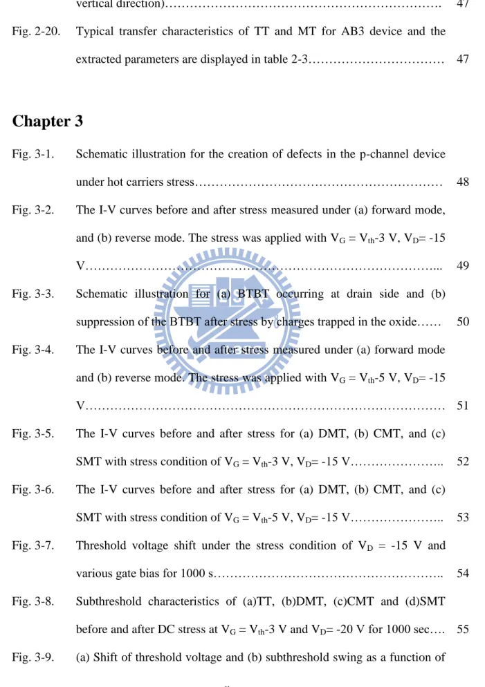
Table 2-1. Dimensions of two types of HC-TFT testers……… 16 Table 2-2. Performance parameters extracted from Fig. 2-8………. 16 Table 2-3. Major parameters extracted from Fig. 2-19……….. 16
Figure Captions
Chapter 1
Fig. 1-1. The formation process for MILC [17]……….. 33
Chapter 2
Fig. 2-1. MILC process of -Si with Ni as the seed………... 34 Fig. 2-2. (a) Symmetrical and (b) asymmetrical seeding window arrangements…... 34
Fig. 2-3. Cross-sectional view of poly-TFT device……… 35
Fig. 2-4. SEM top view of a MILC sample. Enlarged views of the sample showing (b) the interface of MIC/MILC and (c) intersection of SPC/MILC………. 35 Fig. 2-5. Top view of HC-TFT device and the various dimension parameters are
displayed in table 2-1……… 37
Fig. 2-6. (a) Test transistor (TT) and (b) monitor transistors (MTs) (the darker
parts) embedded in a HC-TFT……….. 37
Fig. 2-7. HC-TFT test structures with (a) asymmetric seeding window (ASW) and
(b) symmetric seeding window (SSW)……… 38
Fig. 2-8. Comparisons of transfer characteristics between SPC and MILC devices and the performance parameter are summarized in table 2-2………... 38
ix
Fig. 2-9. Forward and reverse transfer characteristics of (a) ASW and (b) SSW
devices……….. 39
Fig. 2-10. Typical transfer characteristics of ASW and SSW devices with channel length of (a) 0.6, (b) 2, and (c) 10 μm……….. 40 Fig. 2-11. The effect of channel length on (a) threshold voltage (Vth) and (b)
subthreshold swing (SS) of ASW and SSW devices……… 42 Fig. 2-12. SEM picture for the region of DMT in an HC-TFT with ASW. (B1 type
with structural parameters listed in Table 2-1)………. 43 Fig. 2-13. SEM picture for the region of CMT in an HC-TFT with ASW (B1 type).
Channel length of this device is 10m, and the region is about 10~11 m
away from the seeding window……… 43
Fig. 2-14. SEM picture for the region of SMT in an HC-TFT with ASW (B1 type). Channel length of this device is 10m, and the region is about 14~15 m
away from the seeding window……… 44
Fig. 2-15. Transfer characteristics of SMT, CMT and DMT in an HC-TFT with
ASW (B1 type)………. 44
Fig. 2-16. Defect-rich region formed in the SSW device (conventional device). Channel length of this device is 10m, and the region is at the central of
channel………... 45
Fig. 2-17. Transfer characteristics of SMT, CMT and DMT in an HC-TFT device
with SSW (B1 type)………. 45
Fig. 2-18. SEM pictures of the poly-Si channel in the middle region of CMT in an HC-TFT with SSW (B1 type). The magnification ratio is (a) 50k X and
(b) 60k X……….. 46
x
along the horizontal direction) and a monitor transistor (MT, along the
vertical direction)………. 47
Fig. 2-20. Typical transfer characteristics of TT and MT for AB3 device and the extracted parameters are displayed in table 2-3……… 47
Chapter 3
Fig. 3-1. Schematic illustration for the creation of defects in the p-channel device
under hot carriers stress……… 48
Fig. 3-2. The I-V curves before and after stress measured under (a) forward mode, and (b) reverse mode. The stress was applied with VG = Vth-3 V, VD= -15
V………... 49
Fig. 3-3. Schematic illustration for (a) BTBT occurring at drain side and (b) suppression of the BTBT after stress by charges trapped in the oxide…… 50 Fig. 3-4. The I-V curves before and after stress measured under (a) forward mode
and (b) reverse mode. The stress was applied with VG = Vth-5 V, VD= -15
V……… 51
Fig. 3-5. The I-V curves before and after stress for (a) DMT, (b) CMT, and (c) SMT with stress condition of VG = Vth-3 V, VD= -15 V……….. 52
Fig. 3-6. The I-V curves before and after stress for (a) DMT, (b) CMT, and (c) SMT with stress condition of VG = Vth-5 V, VD= -15 V……….. 53
Fig. 3-7. Threshold voltage shift under the stress condition of VD = -15 V and
various gate bias for 1000 s……….. 54
Fig. 3-8. Subthreshold characteristics of (a)TT, (b)DMT, (c)CMT and (d)SMT before and after DC stress at VG = Vth-3 V and VD= -20 V for 1000 sec…. 55
xi
stress drain bias under the stress condition of VG = Vth – 3 V for 1000 sec. 56
Fig. 3-10. Subthreshold characteristics before and after DC stress at (a) VG = Vth -
3V, VD= -20 V and (b) VG = Vth-3 V, VD= -15 V for 1000 sec………… 57
Fig. 3-11. Degradation of (a) on-current and (b) subthreshold swing, and (c) shift of threshold voltage under the stress condition of VD = -20 V and various
gate bias for 1000 sec………... 58
Fig. 3-12. Transfer characteristics of the TT with various applied drain bias……….. 59 Fig. 3-13. Schematic illustration for band diagrams at VG = 0 V and VD= -20 V
along (a) vertical direction (located in the drain/gate overlap region of the TT) and along (b) channel direction, respectively, in which the BTB tunneling and FN tunneling processes are described………... 60 Fig. 3-14. Shift of threshold voltage, and (b) degradation of on-current and (c)
subthreshold swing as a function of stress time. The stress condition is VG
= Vth – 3 V and VG = -20 V……….. 61
Fig. 3-15. Subthreshold characteristics of DMT before and after DC stress at VG =
Vth-3 V and VD= -20 V for various time………... 62
Fig. 3-16. Subthreshold characteristics for an SPC test transistor before and after stress measured under (a) forward mode and (b) reverse mode under stress condition of VG = Vth-3 V and VD= -20 V for 1000 sec. [35]……… 63
Fig. 3-17. Subthreshold characteristics of (a) DMT, (b) SMT, and (c) CMT embedded in an SPC test device before and after stress under stress condition of VG = Vth-3 V, VD= -20 V for 1000 sec. [35]……… 64
Fig. 3-18. (a) Shift of threshold voltage, and (b) on-current degradation as a function of stress drain bias for SPC devices under the stress condition of VG =
xii
Fig. 3-19. Schematic illustration for energy distribution of channel carriers in MILC and SPC devices under the same hot carrier stress condition……….. 66 Fig. 3-20. Degradation of on-current as a function of stress drain bias for SPC
devices under the stress condition of VG = Vth – 3 V for 1000 sec……….. 67
Fig. 3-21. Degradation of on-current as a function of stress drain bias for MILC devices under stress condition of VG = Vth – 3 V for 1000 sec……… 67
1
Chapter 1
Introduction
1.1 Overview of Polycrystalline Silicon Thin-Film
Transistors
In the past, the mainstream device technology used in active-matrix liquid-crystal displays (AMLCDs) was amorphous silicon thin-film transistors (α-Si TFTs) due to the advantages of low temperature fabrication process and the compatibility with low-cost glass substrates [1]. However, the low electron field-effect mobility (< 1 cm2V-1s-1) in α-Si TFT limits its further development in driver integrated circuits on the active matrix plate. In this regard, the superior field-effect mobility achievable with low temperature polycrystalline silicon (poly-Si) is seen to be essential to integrating the driving circuits on the same glass substrate for
better performance of system and cost reduction.
With the advantages of higher field-effect mobility [2], a variety of applications of poly-Si TFTs in addition to the AMLCD [3][4]have been widely investigated, such as high-density static random access memories (SRAMs) [5], electrically erasable programmable read-only memories (EEPROMs) [6], sensors [7] and 3-D ICs’ [8]. However, as compared with single-crystalline silicon, poly-Si suffers from structural defects mostly distributed in or near the grain boundaries that act as charge-trapping centers and greatly affect the transport of carriers in the poly-Si TFTs [9]. Accordingly, the electric characteristics in poly-Si thin film transistors will be inferior
2
to single crystalline counterparts. In order to improve the quality of the active layer, several methods such as excimer laser annealing (ELA) [10] and metal-induced lateral crystallization (MILC) [11] have been developed.
1.2 Formation of Polycrystalline Silicon
Among the various techniques for preparing poly-Si, solid-phase crystallization (SPC) and ELA have been the most frequently used. SPC is a most common method to transform α-Si to poly-Si at a temperature (typically 600 ℃) for several hours. However, there are some issues remained. First, the crystallization temperature is a little bit high and approaches the limit that the glass substrate can tolerate. Moreover, the grain size is not large thus the fabricated device characteristics are affected. To address these issues, ELA is proposed and have become an important manufacturing technique for low-temperature poly-Si (LTPS) applications.
1.2.1 Laser Crystallization
The ELA is suitable for low-temperature fabrication process due to the use of excimer laser as a heating source for crystallization. This method uses short-duration pulsed lasers (10-30 ns) operating in the ultraviolet waveband to irradiate the α-Si. Due to the reason that the radiation is strongly absorbed by α-Si and the short pulse time results in small heat diffusion length, partially α-Si will melt [12]. With an appropriate adjustment in process conditions, good quality of active layers with enlarged grains can be obtained. As a result, the field-effect mobility is enhanced as well.
3
drawbacks that need to address. For example, the rather high manufacturing cost, the uniformity of the poly-Si grain size and its impact on the variation of device performance, and the bulges formed at the borders between two grains which degrade the surface roughness and gate dielectric reliability performance [13]. These issues can be relieved with newly developed scheme, i.e., the MILC, which is described below.
1.2.2 Metal-Induced Lateral Crystallization (MILC)
Conventionally, SPC is used to transform α-Si to poly-Si at around 600 ℃ with a considerable process time (up to tens of hours). When some metal species are added into α-Si as catalyst, the crystallization temperature or the process time can be significantly lowered. It is because the metal elements such as Al [14], Pd [15], or Ni [16] can lower the energy barrier of transformation between α-Si and poly-Si by forming a metal silicide, by eutectic alloy formation, or by migration of metal silicide [14]. Such phenomenon is known as metal-induced crystallization (MIC).
In fact, not all metals can act as an appropriate catalyst to form high-quality active layer. For example, Al will form eutectic alloy with intrinsic silicon with serious metal contamination [16], and the crystalline quality with Pd doping is not satisfactory for device applications [15]. In other words, if a metal exhibits characteristics such as high diffusion speed in α-Si, not degrading the quality of active layer, and lowering the crystallization temperature, it will be suitable to being added into α-Si for LTPS preparation. In this study, we use nickel for the experiments since it meets these requirements.
As a silicon layer with an ultra-thin nickel film deposited on its surface experiences a thermal anneal, the octahedral NiSi2 phase, acting as the sites for
4
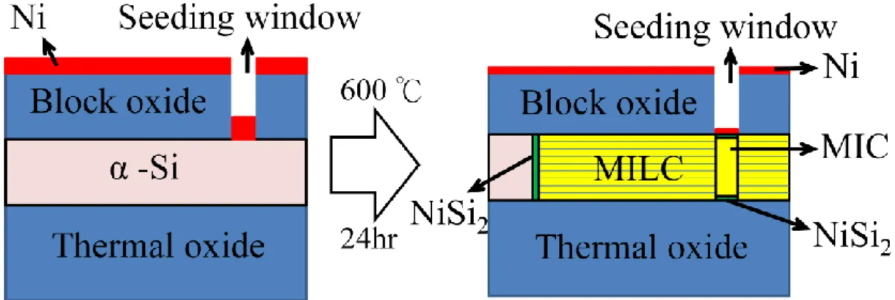
crystallization, is formed in the α-Si matrix. With the presence of nickel silicide, a large number of small and spherical grains grow below the nickel layer by the so called “metal induced crystallization”. Then NiSi2 migrates through whole α-Si, and
the needlelike poly-Si grains are subsequently resulted, as shown in Fig. 1 [17]. Such scheme is called “metal-induced lateral crystallization” (MILC). It develops along the lateral direction of MIC until impediments are generated as SPC grains start to nucleate and grow [13] [14]. In other words, the incubation time of SPC process limits the length of MILC grains. For this reason, it was proposed to use pulsed rapid thermal annealing (RTA) to carry out the MILC process at a higher temperature by taking advantage of the fact that the thermal time for each pulse is too short to trigger the SPC [17].
In comparison with ELA, MILC film has the advantages of smoother surface, better grain uniformity, and lower cost. MILC films also have larger grain size and higher carrier mobility over SPC ones. However, MILC films are highly susceptible to metal contamination, which will lead to severe leakage current. To resolve this problem, some people proposed the use of phosphorous as gettering centers to trap nickel atom and reduce its concentration inside the film, while others used multi-gate structure to improve performance [18].
1.3 The Reliability Issues
The stability of device characteristics under long-term operation is important for circuit applications. In comparison with conventional MOSFETs, the reliability issue will be different in LTPS TFT because of the unique and the intrinsic material properties of crystallized poly-Si.
5
1.3.1 The Process-related Issues
Generally, some reliability issues are related to fabrication processes. First, the gate oxide used in LTPS TFTs is typically deposited at low temperature by CVD methods. The quality of gate oxide, which is deposited by CVD, in LTPS TFT has poorer physical and electrical quality than thermal gate oxide in single-crystal Si MOSFETs. Moreover, mobile ions, Si-OH and/or Si-H bonds, and fixed charges are more likely to show up in gate oxide for LTPS [19-21]. Second, Poly-Si contains many weak strained Si-Si bonds and dangling bonds inside or near the grain boundaries. The dangling bonds act as carrier trapping centers and degrade carrier transport dramatically. During device operation, the strained bonds can be easily broken and become newly created defect inside the channel and result in the change in device characteristics [22].
1.3.2 Degradation under Operation
Degradation in characteristics of solid-state devices under stress tests such as hot-carrier effect [23] and self-heating effect [24] was well-known and widely reported. The degradation caused by hot carriers generated from the high electric field near the drain junction has been widely investigated in MOSFETs. In this condition, carriers in the channel, which are converted to “hot carriers” by gaining energy from high electric field, will cause local damage at the interface between the channel and the gate oxide [25]. In poly-Si TFTs, hot carriers also damage the weak bonds in grain boundary, and create many new defect states to result in serious degradation of device characteristics [23]. Therefore, the degradation mechanisms of poly-Si TFTs strongly depend on the amount of grain boundary in the channel.
6
Another important degradation event induced during device operation is self-heating. Since the glass substrate is a poor thermal-conducting media, heat generated during device operation is difficult to dissipate. As the devices are operated under ON-state with high bias conditions, the device temperature can be raised to a degree that some weak bonds in poly-Si TFT will break. In general, wide-channel TFTs and/or small-size TFTs suffer more seriously from self-heating [24].
1.4 Motivation of this Study
To realize the high-performance characteristics and low-temperature fabrication process for thin film transistors in AMLCD’s application, the MILC process appears to be a viable choice to reach the goals without adding too much production cost [12]. For the purpose of using MILC process, it is important to clarify the relationship between the orientations of needlelike grains and device characteristics, and understand the effects relevant to the metal added. Furthermore, due to the unique granular structure, the reliability issues in MILC devices may differ from SPC devices, so it is also imperative to clarify the degradation mechanisms in MILC. Moreover, the studies on p-channel MILC TFTs are few to this date.
In the past, indeed some research efforts have been devoted to the degradation mechanisms of hot-carrier stress for MILC devices. The results indicated that the damage regions were quite localized in the channel by using simulation or special designs of measurements [23] [26]. However, all of these methods cannot directly resolve the location-dependent damage characteristics. For long-channel devices, the possibility of forming both MILC and SPC granular structures inside the same channel may further complicate the situation.
7
[27] [28] to study the hot-carrier effects of p-channel LTPS TFTs. The unique tester, introduced in Chapter 2, is designed for spatially resolving the non-uniform characteristics along the channel. With such capability, it is employed in this thesis to investigate the hot-carrier degradation caused by either DC (static) or AC (dynamic) stress tests for p-channel LTPS TFTs.
1.5 Thesis Organization
There are four chapters in the thesis. In Chapter 1, the application of LTPS TFTs, three kinds of LTPS preparation techniques, and the associated reliability issues are briefly introduced. In the next chapter, we describe the novel test structure, its fabrication process, and its capability in resolving the location-dependent device characteristics before and after the hot-carrier tests.
In Chapter 3, results of the reliability characterization under DC (static) stress condition are presented and analyzed by using the novel test structure. Major focus is to pinpoint the location where major damage region is induced and identifies its degradation mechanism. A comparison and discussion of the degradation mechanisms between SPC and MILC devices are also given. Finally, we summarize the conclusion and suggest future work in Chapter 4.
8
Chapter 2
Fabrication and Electrical
Characteristics of MILC Devices
2.1 Device Fabrication and Operating Principle of
HC-TFTs
First, six-in. silicon wafers covered with 100nm-thick thermal oxide were used as the starting substrates, followed by deposition of a 100nm-thick α -Si film with low-pressure chemical vapor deposition (LPCVD) at 550 ℃. Then, a 100nm-thick low temperature oxide deposited by plasma enhanced chemical vapor deposition (PECVD) was used as a block layer. After formation of the seeding windows, a thin 5nm Ni layer was deposited by E-gun, followed by 540 ℃ thermal annealing in furnace for the purpose of MILC crystallization, as shown in Fig. 2-1. In this thesis, two splits of seeding window arrangement were exploited, as shown in Fig. 2-2. In one split, the window was opened only at the drain region, denoted as Asymmetric Seeding Window (ASW), while the other one has the windows opened at both source and drain regions, denoted as Symmetric Seeding Window (SSW).
After finishing MILC process, we removed the Ni layer and block oxide by wet etching steps. Then a 30nm-thick PECVD oxide for gate dielectric and a 150nm-thick LPCVD poly-Si gate material were deposited. Next, after accomplishing gate patterning and exposure of the source and drain regions, the source, drain, and gate regions were doped by self-aligned BF2+ implantation at a
9
dose of 5×10¹⁵ /cm2 and energy of 50 keV. Dopant activation was performed at 600 ℃ for 12 hours by furnace, and then a PECVD oxide layer of 200 nm was deposited andused as the passivation layer to prevent the penetration of humidity and impurity. Finally, contact-hole patterning and metallization steps were performed, followed by a sintering treatment at 400 oC for 30 min. Figure 2-3 shows the final cross-section of TFT devices. The SPC device fabrication is similar to MILC device except the crystallization of the active layer: the SPC split skipped the Ni seed deposition and transformed the Si channel layer from α-Si to poly-Si by a thermal treatment done at 600 ℃ for 24 hours in furnace.
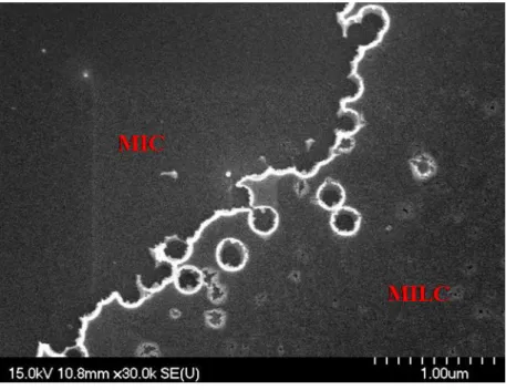
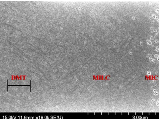
One test wafer was used to analyze the granular texture after MILC process. Prior to taking the SEM pictures, the specimens were soaked in Secco etch for 25 seconds. Some of the results are shown in Figs. 2-4 (a) ~ (b). In Fig.2-4(a), upper left corner shows MIC grains, right lower corner shows SPC grains, and in between is the MILC region which contains needle-like grains. Enlarged views of the regions close to the MIC/MILC and MILC/SPC interfaces are shown in Figs. 2-4(b) and 2-4(c), respectively.
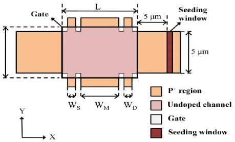
In this thesis, two kinds of devices were characterized for better understanding of the impacts of MILC process on device performance. In addition to the conventional layout schemes shown in Fig. 2-2 which are used for measuring basic characteristics and investigating the effects of channel length, width, as well as the arrangement of the seeding windows, the other type is termed HC-TFT with the layout scheme shown in Fig. 2-5, which is configured with four pairs of p
+
electrodes at the edges of the channel. Major dimensional parameters are listed in Table 2-1. Roles of each components embedded in the test structure can be clearly understood with the help of Figs. 2-6(a) and 2-6(b). In the x- (i.e., horizontal) direction of Fig. 2-6(a), one pair of
10
p+ regions located at the two edge sides of lateral channel in the HC-TFT is called the “test transistor” (TT), which imitates the channel of a conventional device. The other three pairs paralleled in the y-(i.e., vertical) direction construct three transistors called “monitor transistors” (MT), as shown in Fig. 2-6(b), which are capable of analyzing the asymmetrical and location-dependent degradation along the channel of test transistor (TT) caused by the MILC process and the HC stress testing. As can be seen in the figures, the TT and MTs share a common gate electrode lying over the entire channel. Therefore, the localized change along the test transistors, caused by structural issue of needle-like MILC grains in the channel or damage under bias stress, can be characterized by probing the current-voltage (I-V) characteristics of the corresponding MT. In Fig. 2-6(b), according to their position relative to the channel of the test structure, the three MTs are denoted as SMT (i.e., source-side MT), CMT (i.e., central MT), and DMT (i.e., drain-side MT). As aforementioned, the ASW and SSW splits for location of seeding windows are also established in HC-TFTs, as shown in Fig. 2-7(a) and Fig. 2-7(b), respectively.
2.2 Measurement Setup
The subthreshold and output characteristics were measured by a Keithley 4200 semiconductor characterization system with Keithley Interactive Test Environment (KITE) software. During the process of measurement, temperature- regulated hot chuck was maintained at 30 ℃.
The major electrical parameters of devices can be extracted from the measurement of I-V curves. The threshold voltage, denoted as “Vth”,is defined as the
11
width and channel length, respectively. The subthreshold swing, denoted as “SS”, is calculated by the following equation:
SS = . (Eq. 2-1) Moreover, the change of threshold voltage (Δ Vth) and subthreshold swing (Δ SS)
after bias stressing are calculated by the equations: Δ Vth = Vth,stress - Vth,fresh,
Δ SS = SSstress - SSfresh, (Eq. 2-2)
where the notation “fresh” and “stress” refer to the conditions before and after stressing, respectively. The on-current (Ion) is defined as the value ID at VG = -10V.
After stressing, the deviation of on-current is formulated by (ΔIon / Ifresh) × 100%.
Similarly, ΔIon = Ion,stress – Ion,fresh, where Ion,stress is defined as the value at VG= -10+Δ
Vth. Finally, the field-effect mobility (μFE) is estimated by gm,max, which is described
by the following equations.
gm =
,
μFE =
(Eq.2-3)
where Cox is the capacitor of gate insulator.
2.3 Basic Electrical Characteristics
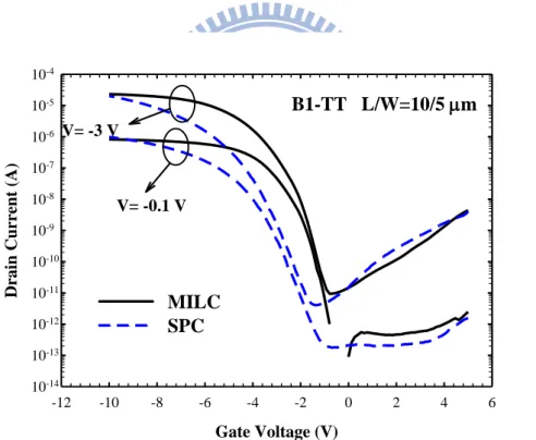
It is well known that the active layer prepared by MILC process takes advantage of needle-like grains directing across the channel from drain to the source, and the reduction in the quantity of trapped centers improves the carrier mobility as well as the device performance [29]. Fig. 2-8 shows the ID-VG curve for MILC and SPC
12
characteristics in terms of higher carrier mobility, lower Vth and SS as compared with
the SPC one. The extracted performance parameters are summarized in Table 2-2. According to the results, it is illustrated that a smaller grain size (in average) and absence of directional arrangement of grains along the channel degrade the performance of SPC devices [30].
It seems that MILC devices have better electrical characteristics than the SPC one. However, one disadvantage in application is the enhancement of leakage current arisen from metal contamination. This condition can be understood in Fig. 2-9(a) by comparing the difference in off-state ID between forward and reverse modes. Here the
“forward mode” denotes the case when the drain bias is applied to the heavily doping region where seeding window is located while the other electrode without seeding window is grounded and serves as the source. For “reverse mode” of operation, the above arrangement is simply interchanged. The leakage current is obviously higher under forward mode in the ASW device, as shown in Fig. 2-9(a). However, such difference is unobserved for the SSW device, whose leakage current is consistent between the two modes, as shown in Fig. 2-9(b). Note the leakage levels in the present case are high and comparable to that of the forward mode exhibited in the ASW device (Fig. 2-9(a)). These high leakage levels can be attributed to the existence of nickel-rich phases near the junction region. The contamination tends to induce additional defect levels inside the channel layer which are responsible for the increased leakage current. These defects act as generation centers and enhance the leakage at low VD via trap-assisted thermal generation process, and the leakage at
high VD via trap-assisted field emission [31] [32]. As a result, the issue of metal
contamination in MILC device must be considered to prevent the undesirable increase of leakage current. In this thesis, the offset region between gate edge and seeding
13
window is set at 5 m. As compared with self-aligned seeding arrangement, such offset can help reduce the number of nickel at the junction of drain [31].
2.4 Effects of Channel Length and Seeding Window
Configuration
As mentioned above, the film crystallinity of a MILC film is location-dependent and related to distance from the seeding window as well as the seeding window arrangement. Certainly such property will draw impacts on device performance and worth investigation.
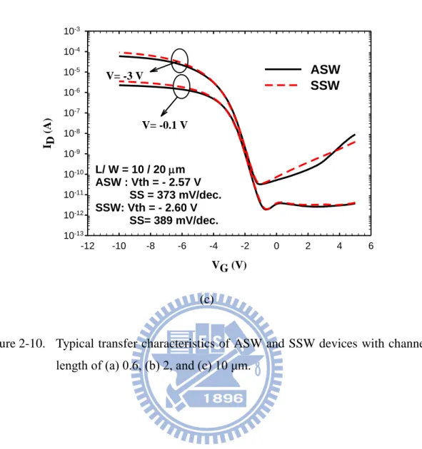
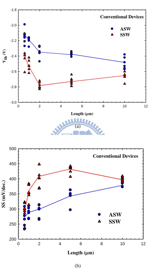
Figures 2-10(a), (b), and (c) show typical transfer curves of SSW and ASW devices with channel length at 0.6, 2, and 10 μ m, respectively. Threshold voltage (Vth) and subthreshold swing (SS) of the two types of device as a function of channel
length (L) are shown in Figs. 2-11(a) and (b), respectively. In Fig. 2-11(a), the ASW devices show Vth roll-off phenomenon, seeming to indicate the occurrence of
short-channel effect. However, the SS shown in Fig. 2-11(b) improves with decreasing channel length, indicating that better film crystallinity in shorter-channel devices also accounts for the Vth reduction as compared with long-channel ones. On
the other hand, the SSW devices generally exhibit worse performance in terms of higher Vth (absolute value) and SS than ASW ones at the same Length. Interestingly,
the difference between the two types of devices is most significant at L of 2 and 5 m, and diminishes as L either decreases or increases.
From the above, it is seen that devices with shorter channel have superior Vth and
SS to long channel ones. Such outcome is believed to arise from the variation in film crystallinity across the channel. To confirm this we performed SEM analysis on a B1 HC-TFTs (see Table 2-1) with ASW to check the film crystallinity in different regions
14
of the channel. Excellent crystalline quality can only be observed in the DMT region which is most close to the MIC area, as shown in Fig.2-12.In this picture the surface looks quite flat that the grain boundaries are hardly resolved.In the range of CMT, the appearance of needle-like grains can be observed in Fig. 2-13, where the grain size is obviously smaller than that in the DMT region. Finally, at the source side, as shown in Fig. 2-14, it is apparent that the grains already become smaller and discrete, a feature associated with the occurrence of the SPC process [32].
The differences in film crystallinity actually reflect on the electrical characteristics of the monitor transistors, as shown in the Fig. 2-15. It is clear that the best performance among three monitor transistors is DMT and the worst one is SMT, confirming the difference in film quality examined with the SEM technique.
In Fig. 2-11, it is observed that the Vth and SS for the SSW devices are inferior to
the ASW ones. This is believed to be related to the intersection of the two MILC fronts growing from the two seeding windows located at source and drain regions. One SEM evidence is given in Fig. 2-16. This picture was taken from an SSW device and a defect-rich region is clearly observed in the middle of the channel. The abundance of defects acting as trap centers will degrade device characteristics [33]. Such defect-rich region draws different impact on devices with various channel length, as shown in Fig. 2-11(b) where the SS for SSW improves with decreasing length. This is mainly attributed to the improved crystallinity as the channel region gets closer to the seeding windows as analyzed in the ASW case. On the other hand, as L is increased from 5 to 10 m, the SSW devices characterized in Figs. 2-11(a) and (b) show slightly decreased Vth and SS and reduce the difference with the ASW ones.As
have been shown in Fig. 14, SPC granular structure is predominant at the central part of the channel for such long-channel devices. This would dilute the impact of the
15
aforementioned defect-rich region on the device performance and explain why the difference between the ASW and SSW devices diminishes.
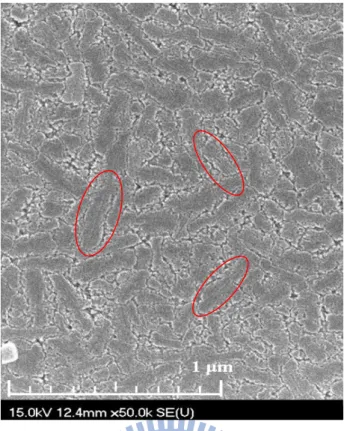
The above inference can be verified from the I-V curves of MTs embedded in an SSW HC-TFT shown in Fig. 2-17 and SEM pictures in Fig. 2-18. The measured results in Fig. 2-17, which has been normalized to the channel width, clarify the much superior performance in DMT and SMT to that of CMT. Figure 2-18(a) shows obvious jagged granular structure resulted in the middle of a CMT due to the confrontation of the two MILC fronts, and it signifies that many grain boundaries have been formed in the neighborhood of jagged structure. An enlarged view illustrated in Fig. 2-18(b) displays that there are many defects and sprawl grains near the jagged structure. Existence of such defect-rich region certainly impacts the device characteristics.
It is also worthy to know the impacts of granular structure of the poly-Si films on device characteristics, such as the lying orientation of needle-like grains as well as the location-dependent film crystallinity,are probed by a special test device shown in Fig. 2-19. In the device, in addition to the TT, an MT is also embedded with its source-to-drain direction vertical to the TT. Typical transfer characteristics are shown in Fig. 2-20, in which the drain current has been normalized to the channel width. It can be observed that the on-current of the TT is higher than that of the MT. The extracted parameters are summarized in Table 2-3. It can be seen that TT exhibits higher on-current and field-effect mobility than the MT. This is primarily attributed to the reduced number of grain boundaries counted from source to drain in the TT than that in the MT, owing to the needle-like grains originating from the seeding window [34].
16
Table 2-1. Dimensions of two types of HC-TFT testers.
Table 2-2. Performance parameters extracted from Fig. 2-8.
Table 2-3. Major parameters extracted from Fig. 2-19.
17
Chapter 3
Hot Carrier Degradation
under Static Stress
In order to study the degradation induced in MILC devices due to hot-carrier effects, various static stress conditions were executed on the HC-TFTs. The change in the characteristics of test transistor and monitor transistors were recorded and analyzed. The difference between MILC and SPC devices were resolved by taking advantage of HC-TFTs.
3.1 Hot Carrier Stress under Mild Stress Bias
Mechanisms of hot-carrier degradation in p-channel MILC devices are similar to other types of poly-Si TFTs with the schematic shown in Fig. 3-1. This figure illustrates that holes obtain energy from the high electric field near the drain junction to form “hot carriers”. As the energy of the hot holes is sufficiently high, impact ionization process may trigger and generate electron-hole pairs. Some of the generated electrons may become energetic and surmount the barrier height at the oxide interface and then inject into gate insulator to form negative oxide trap charges which cause positive shift in threshold voltage. The hot carriers may also release their energy near oxide/channel interface and in the channel, and leave additional defects and interface states therein which will degrade the subthershold swing and mobility.
18
before and after DC stress. The stress testing was done under VD = -15 V and VG = Vth
- 3 V for 1000 s. It can be observed that the only obvious change before and after stress for the I-V curve in Fig. 3-2 (a) is the off current, which is suppressed under the forward mode and becomes independent of the gate bias. Under the reverse mode, the I-V curves before and after stress resembles each other with negligible change. In the figures the fresh device exhibits an off current which increases with increasing difference between the drain voltage and the gate voltage, a feature characteristic of band-to-band tunneling (BTBT) conduction process shown in Fig 3-3(a). In the figure direct BTBT is assumed, in the present case the defects presenting in the poly-Si layer would contribute to the trap-assisted paths and further enhance the conduction. As aforementioned, some electrons would be generated by impact ionization near the drain junction and then got trapped in the gate oxide near the drain junction. The negative charges would raise the local potential, relieve the electric field and suppress the BTBT current, as shown in Fig. 3-3(b). This explains the suppression of off-state current in Fig. 3-2(a) after the stress. For the reverse mode shown in Fig. 3-2(b), the nominal source now is where BTBT is taking place and the current is not affected since negligible electrons are trapped wherein.
In fact, it is hard to obtain sufficient information to resolve the degree of degradation under hot-carrier stress just by analyzing the forward and reverse modes of transfer curves, and also hard to conceive details about the location-dependent damage in the device. For example, Figs. 3-4(a) and (b) show the device characteristics before and after stress with stress condition the same as that of Fig. 3-2 except with a different gate bias VG = Vth - 5 V. The information revealed in the
figures is basically the same as that given in Figs. 3-2(a) and (b) and cannot distinguish the major impact resulting from the use of different gate bias during
19
stressing. However, the monitor transistors contained in the HCTFTs can be used to break such constraint. Fig. 3-5 and Fig. 3-6 show the characteristics of the monitor transistors of the devices characterized in Figs. 3-2 and 3-3, respectively. As can be seen in the figures, the major difference arising from different gate stress voltage is clearly reflected on the characteristics of DMT. Specifically, the lower gate bias (absolute value) under hot carrier stress operation has resulted in a larger shift in the threshold voltage of the DMT shown in Fig. 3-5(a), as compared with that shown in Fig. 3-6(a). Obviously the different outcomes are related to the amount of electrons trapped in the oxide. During the stress with identical VD, (e.g., -15V), an increase in
gate voltage reduces the voltage drop between drain and gate (ie. VD-VG) and
therefore the electric field in the gate oxide therein reduces as well. As a result, the probability of electron injecting into the oxide is slashed and causes smaller shift in the threshold voltage, as shown in Fig. 3-6(a). Such effect associated with stress gate bias can be more clearly understood from the results illustrated in Fig. 3-7. In the figure we can find that the shift in threshold voltage is noticeable only in the DMT and increases with decreasing VG.
3.2 Hot Carrier Stress under Severe Stress Bias
Compared to the mild stress drain voltage investigated in last section, a raised drain voltage will increase not only the lateral electric field to enhance the impact ionization but also the vertical electric field. The latter would result in more electron trapping events as well as more generated interface states. To illustrate such impacts, we stressed the TT with a high VD of -20 V and VG = Vth - 3 V for 1000 s. In this case,
the device characteristics of the TT shown in Fig. 3-8(a) exhibit similar trend revealed in Fig. 3-2(a) and Fig, 3-4(a). However, in Fig. 3-8(b), the I-V curves of the DMT
20
deviate significantly after the stress, while negligible changes are found in the results of CMT and SMT as shown in Fig. 3-8(c) and Fig. 3-8(d), respectively. When a comparison is made between Fig. 3-5(a) and Fig. 3-8(b), it is clear that a larger positive shift in Vth is resulted as the stress drain voltage is increased, arising from the
increase of electron injection in the gate oxide. Figs. 3-9(a) and (b) show the shift in Vth and SS as a function of the stress drain voltage. It can be seen that increasing
electron trapping in the DMT with increasing stress drain voltage stated above is clearly illustrated in Fig. 3-9(a). Another major impact is the increase in SS for the DMT devices, as shown in Fig. 3-9(b). This phenomenon can be better understood with the I-V curves shown in Figs. 3-10(a) and (b),in which the drain currents of the DMTs depicted in Fig. 3-8(b) and Fig. 3-5(a), respectively, are expressed as a function of gate overdrive (VG-Vth). The inferior characteristics arise mainly from the
generation of additional defects in the channel and interface states at oxide/channel interface. With higher stress drain voltage, the resultant damage is stronger in term of worse SS, as evidences in Figs. 3-9(b), 3-10(a), and 3-10(b).
As aforementioned, the raise in stress Vg would alleviate the vertical electric field in the oxide near the drain junction to reduce the amount of trapped electrons. However, such damage is minor as the stress drain voltage is mild and hard to detect with the TT only. It thus needs a high stress drain voltage to resolve the degradation mechanism. Figures 3-11(a), (b) and (c) show the on-current, SS degradation, and Vth
shift, respectively, of TT and MTs contained in this tester as a function of stress VG
with VD = -20 V for 1000 sec. It can be seen that the DMT shows the highest
sensitivity to the applied stress conditions. In Fig. 3-11(c), it is interesting to see that the Vth shift of DMT monotonically increases with decreasing VG, which can be used
21
This is owing to the increase in (VG - VD) as VG becomes smaller, so that the strength
of electric field in the gate oxide of the DMT increases. For VG = 0, the high field
strength would result in significant F-N tunneling process, resulting in significant degradation in SS and Vth shift. However, the SS degradation shown in Fig. 3-11(b)
exhibits a dip at VG = -2.5V. Such trend is different from that shown in Figs. 3-11(a)
and (c). To more clearly understand such disparity, we examine the subthreshod characteristics of the TT device under various VD. We can see that, at VG = 0, a
significant GIDL current which is comparable or even higher than that at VG = -2.5V
is observed. This means that additional carriers are present in the channel during stressing at VG = 0 which may become energetic and result in damage. However, the
damage mechanism is presumably different from that of normal channel hot carrier effects when VG is larger than Vth (absolute value). This explains why the SS
degradation trend shown in Fig. 3-11(b) is different from that of on current degradation and Vth shift.
Band diagrams at VG = 0 along the vertical direction (located in the DMT) and
along channel direction are illustrated in Figs. 3-13(a) and (b), respectively, in which the band-to-band tunneling process is described. That is, due to the strong drain bias, a portion of the electrons generated by BTB tunneling would not only cause impact ionization near the drain junction but also tunnel or surmount the barrier height at the oxide interface and then get trapped in the oxide. On the other hand, most of the electrons would drift along the channel and contribute to the GIDL shown in Fig. 3-12. The voltage drop occurs mainly in the DMT region, and it is believed that these electrons may degrade the channel as they drift through the DMT region. This would result in aggravated SS degradation observed in Fig. 3-11(b)
22
degradation, and SS degradation, respectively, with stress time under stress condition at VG = Vth - 3 V and VD = -20 V. For DMT, the change of Vth (Fig. 3-14(a)) mainly
occurs in the beginning and tends to saturate as the stress time is sufficiently long. This can be more clearly understood with the transfer curves of the DMT shown in Fig. 3-15. Such saturation is reasonable owing to the trapping of the electrons which causes the shift of Vth and consequently a reduction in the vertical electric field in the
oxide. Similar situation also happens to the cases of on-current and SS degradation described in Fig. 3-14(b) and Fig. 3-14(c).
3.3 Hot Carrier Effects in MILC and SPC Devices
As aforementioned, due to the reduced number of grain boundaries presenting along the channel, the MILC devices have superior performance over SPC devices. The hot carrier effects in MILC devices have already been analyzed in Sections 3-1 and 3-2. Finally, in this section, we address the difference in post-stress characteristics between MILC and SPC devices. To make a comparison between MILC and SPC devices with nominally identical structural parameters (e.g., channel length/width, gate oxide thickness), stress condition set at VG = Vth - 3 V, VD = -20 V was used.The
results obtained from the SPC devices were mainly measured by Mr. Chen [35] and, in this thesis, are compared with those for MILC devices displayed at Section 3-2.
Figure 3-16 shows I-V curves under forward mode and reverse mode for a SPC device before and after stress. The only change that can be noticed in TT is the off-current under forward mode, similar to the results of MILC devices presented and discussed in Section 3-1. By using the monitor transistors for a detailed analysis with the results shown in Figs.17(a) ~ (c), it can be observed in Fig. 3-17(a) that the change is very slight in DMT, in strong contrast to the case of MILC device subjected to the
23
same stress condition, as shown in Fig. 3-8(b). On the other hand, Fig. 3-17(b) and Fig. 3-17(c) show negligible change before and after stress in CMT and SMT, respectively. The shift in Vth for the TT and MTs of the SPC devices are shown in Fig.
3-18. Compared with Fig. 3-9(a), the Vth shift in the MILC device is larger than that
in the SPC device, indicating that more electrons are trapped in the gate oxide of MILC devices during stressing.
Since the two devices have the same structural parameters and are subjected to the same stress condition, the above difference is clearly related to the film crystallinity of the active layer. It is well known that a poly-Si film with larger grains will reduce the number of grain boundaries presenting inside the film and lower the probability of carrier scattering [11] [15]. Therefore, the mobility of conductive carriers is improved. Accordingly, the conductive carriers under hot carrier stress are more likely to accumulate their kinetic energy and become “hotter”. Since the SPC poly-Si films are relatively fine granular structure as compared with the MILC ones, the scattering of carriers with the grain boundaries is more significant. As a result, the population of carriers with sufficiently high energy to damage the device in the SPC sample should be much smaller than that in the MICL one. Therefore, the average carrier kinetic energy would be higher for MILC devices, as illustrated in Fig 3-19, and the number of electrons with energy higher than 3.1 eV in MILC devices would be larger than in SPC devices. This can be more clearly understood by comparing the shaded region in Fig 3-19. As a result, the probability of surmounting the energy barrier height (3.1 eV) is larger in the MILC samples, and more electrons will get trapped during stressing, rendering a larger the Vth shift. This explains the discrepancy
observed in Fig. 3-9(a) and Fig. 3-18.
24
weak bonds located near the grain boundaries [36] in the channel. Since these bonds are “weak” (with binding energy < 1 eV), they tend to be struck and broken by hot carriers during stressing. It is thus expected that the SPC devices may seriously suffer from trap generation in the channel and lead to SS and on-current degradation. Figures 3-20 and 3-21 display the degradation of on-current as a function of stress drain bias for SPC and MILC devices, respectively. It can be observed that, not only the DMT, the degradation of TT and CMT in the SPC devices is also obvious. This is in contrast to the results of the MILC device (Fig. 3-21) in which only DMT exhibits dramatic change after the stressing. This result is consistent with the argument that the SPC channel additionally suffers from the trap in the channel. While the small change in TT and CMT with large deviation in DMT for MILC devices is believed to be due to the small damage in channel, but substantial damage at the oxide/channel interface near the drain junction. In sum, the p-channel MILC devices under hot carrier stress mostly suffer from the interface state and trapped electron, which will seriously cause the shift of Vth. While the SPC devices mostly suffer from the trap formation in
25
Chapter 4
Conclusion and Suggested Future work
4.1 Conclusion
In this study, by taking advantage of HC-TFTs to analyze the subthreshohld characteristics of poly-Si TFTs fabricated with MILC scheme, the impacts of the location-dependent film crystallinity of the poly-Si films on device characteristics are carefully studied. Moreover, since this unique test structure is also suitable for spatially resolving the location-dependent damage induced by hot carrier stress, the HC-TFTs have also been successfully used in this study to investigate the local change in internal devices during operation.
Our results show that the MILC devices depict superior device characteristics except for the increased leakage current arisen from metal contamination. We also found that the MILC device characteristics are closely related to the distance of its channel layer to the seeding window. We have proven that the ASW shows superior device characteristics if the channel length is short enough so that the SPC mechanism is not triggered. The inferior subthreshohld characteristics in short-channel SSW devices are due to the defect-rich region in the center of the channel. However, in long-channel devices, the occurrence of SPC granular structure in ASW devices will mitigate the merits of MILC process so the device characteristics become similar to the long-channel SSW devices. Finally, the impacts of defect-rich region and SPC granular structure on device characteristics with various channel length are also analyzed with the help of HC-TFTs, and the results are confirmed by SEM pictures.
26
The hot carrier effects under various stress gate bias and stress drain bias have been studied in Chapter 3. In sum, a larger positive Vth shift and more serious
degradation in SS are resulted as the voltage difference between drain and gate (i.e., VD-VG) is increased, arising from the increase of electron injection in the gate oxide
as well as the generation of defects in the channel or at the oxide/channel interface. For the condition with VG = 0 V, VD = -20 V, a portion of the electrons generated by
BTB tunneling would inject into gate oxide by FN tunneling and then get trapped in the oxide.
The difference of hot carrier effects between SPC and MILC devices was also investigated by HCTFTs. Due to the improved mobility of conduction carriers in MILC devices, the conduction carriers under hot carrier stress are more likely to accumulate their kinetic energy. As a result, the probability of surmounting the energy barrier height (3.1 eV) at the oxide/channel interface is higher in the MILC samples under the same stress condition as compared with the SPC ones, and more electrons will get trapped during stressing, rendering a larger Vth shift. On the other hand, SPC
poly-Si films are relatively fine granular structure in nature as compared with the MILC ones. The larger number of weak bonds in its channel could be easily struck and broken by energetic carriers during stressing and lead to the generation of additional defects. As a result, degradation of SS and on-current is worse in the SPC samples.
27
4.2 Suggested Future Work
Although the effects of ASW and SSW on the MILC devices were already investigated in this study, however, the seeding window size and the channel thickness will also affect the film crystallinity but details about the effects remain unclear. To further improve device performance, these effects should be addressed in the future.
The hot carrier stress under the operation of AC mode (i.e., dynamic) is more complex than DC mode, and it is also worthy to study and understand the difference in this regard between the MILC and SPC devices under AC stress. On the other hand, the negative bias temperature instability (NBTI) is another serious reliability issue for p-channel TFTs [37]. The mixed effect of NBTI and hot-carrier effect should be distinguished and evaluated. HC-TFTs should be a viable vehicle for addressing this issue.
28
References
[1] H.C. Tuan, “Amorphous silicon thin film and its applications to large-area elements,” Mater. Rec. Soc. Ump. Proc., vol. 33, pp. 357-362, 1984.
[2] A. Mimura, N. Konishi, K. Ono, J. I. Ohwada, Y. Hosokawa, Y. A. Ono, T. Suzuki, K. Miyata and H. Kawakami, “High performance low-temperature poly-Si n-channel TFTs for LCD,” IEEE Trans. Electron Devices, vol. 36, pp. 351-359, 1989.
[3] N. Ibaraki, “Low-temperature poly-Si TFT technology,” SID Intl Symp Digest Tech Papers, pp. 172-175, 1999.
[4] Y. Oana, “A 240×360 element active matrix LCD with integrated gate-bus drivers using Poly-Si TFTs,” Proc 4th Intl Display Research Conf, pp. 312-315, 1984.
[5] M. Aoki, T. Hashimoto, T. Yamanaka, and T. Nagano, “Large 1/f noise in polysilicon TFT loads and its effects on the stability of SRAM cells,” Jpn. J. Appl. Phys., vol. 35, pp. 838-841, 1996.
[6] N. D. Young, G. Harkin, R. M. Bunn, D. J. McCulloch, and I. D. French, “The fabrication and characterization of EEPROM arrays on glass using a low temperature poly-Si TFT process,” IEEE Trans. Electron Devices, vol. 43, pp. 1930-1936, 1996.
[7] F. J. Gutierrez, L. Ares, J. I. Robla, M. C. Horrillo, and I. Sayago, “Properties of polycrystalline gas sensors based on DC and AC electrical measurements,” Sensors and Actuators Chemical, vol. 8, pp. 231-235, 1992.
[8] K. Banerjee, S. J. Souri, P. Kapur, and K. C. Saraswat, “3-D ICs: a novel chip design for improving deep-submicrometer interconnect performance and
29
system-on-chip integration,” Proceedings of the IEEE, vol. 89, pp. 602-633, 2001.
[9] John Y. W. Seto, “The electrical properties of polycrystalline silicon films,” J. Appl. Phys., vol. 46, pp. 5247-5254, 1975.
[10] T. Sameshima, M. Hara and S. Usui, “XeCl excimer laser annealing used to fabricate Poly-Si TFT's,” Jpn. J. Appl. Phys., vol. 28, pp. 1789-1793, 1989. [11] S.-W. Lee and S.-K. Joo, “Low temperature poly-Si thin-film transistor
fabrication by metal-induced lateral crystallization,” IEEE Electron Device Lett., vol. 17, pp. 160-162, 1996.
[12] S. D. Brotherton, “Topical review: polycrystalline silicon thin film transistors,” Semicond. Sci. Technol., vol. 10, pp. 721-738, 1995.
[13] A. T. Voutsas, “A new era of crystallization: advances in polysilicon crystallization and crystal engineering,” Applied Surface Science, vol. 208-209, pp. 250-262, 2003.
[14] S. Y. Yoon, S. J. Park, K. H. Kim, and J. Jang, “Metal-induced crystallization of amorphous silicon,” Thin Solid Films vol. 383, pp. 34-38, 2001.
[15] S. W. Lee, Y. C. J. eon, and S. K. Joo, “Pd induced lateral crystallization of amorphous Si thin-films,” Applied Physics Letters, vol. 66, pp. 1671-1673, 1995. [16] H. K. Y. Kawazu, S. Onari and T. Arai, “Low-temperature crystallization of hydrogenated amorphous silicon induced by nickel silicide formation,” Jpn. J. Appl. Phys., vol. 29, pp. 2698-2704, 1990.
[17] C. F. Cheng, T. C. Leung, M. C. Poon, and M. Chan, “Large-grain polysilicon crystallization enhancement using pulsed RTA,” IEEE Electron Device Letters, vol. 25, pp. 553-555, 2004.
30
Chang, “High performance metal induced lateral crystallization polysilicon thin-film transistors with multiple nanowire channels and multiple gates,” IEEE Trans. Nanotechnology, vol. 5, pp. 157-162, 2006.
[19] N. Bhat, M. Cao, and K. C. Saraswat, “Bias temperature instability in hydrogenated thin- film transistor,” IEEE Trans. Electron Devices, vol. 44, pp. 1102-1108, 1997.
[20] N. D. Young and A. Gill, “Water-related instability in TFTs formed using deposited gate oxides,” Semicond. Sci. Technol., vol. 7, pp. 1103-1108, 1992. [21] N. D. Young, A. Gill, and I. R. Clarence, “Mobile ion effects in low-temperature
silicon oxides,” J. Appl. Phys., vol. 66, pp. 187-190, 1989.
[22] F. V. Farmakis and C. A. Dimitriadis, “Effects of hydrogenation on the performance and hot-Carrier endurance of polysilicon thin-film transistors,” IEEE Electron Device Letters, vol. 22, pp. 83-85, 2001.
[23] J. Richard Ayres, Stan D. Brotherton, David J. McCulloch and Michael J. Trainor, “Analysis of drain field and hot carrier stability of poly-Si thin film transistors” Jpn. J. Appl. Phys., vol. 37, pp. 1801-1808, 1998.
[24] S. Inoue, H. Ohshima and T. Shimoda, “Analysis of degradation phenomenon caused by self-heating in low-temperature processed polycrystalline silicon thin film transistors,” Jpn. J. Appl. Phys., vol. 41, pp. 6313-6319, 2002.
[25] A. Schwerin, W. Hansch, and W. Weber, “The relation between oxide charge and the device degradation: A comparison study of n- and p- channel MOSFETs,” IEEE Trans. Electron Devices, vol. 34, no. 12, pp. 2493-2500, 1987
[26] S. K. Joo, S. H. Han, I. S. Kang, “The reduction of the dependence of leakage current on gate bias in metal-induced laterally crystallized p-channel polycrystalline-silicon thin-film transistors by electrical stressing,” IEEE Trans.
31
Electron Devices, vol. 54, pp. 2546-2550, 2007.
[27] H. C. Lin, M. H. Lee, and K. H. Chang, “Spatially resolving the hot carrier degradations of poly-Si thin-film transistors using a novel test structure”, IEEE Electron Device Letters, vol. 27, pp. 561-563, 2006.
[28] M. H. Lee, K. H. Chang, and H. C. Lin, “Spatially and temporally resolving the degradation of n-channel poly-Si thin-film transistor under hot-carrier stressing,” J. Appl. Physics, vol. 101, pp. 054518 1-5, 2007.
[29] G. A. Bhat, Z. Jin, H. S. Kwok, and M. Wong, “Effects of longitudinal grain boundaries on the performance of MILC-TFT’s,” IEEE Electron Device Letters, vol. 20, no. 2, pp. 97-99, 1999.
[30] M. Wang, Z. Meng, and M. Wong, “Anisotropic conduction behavior in metal-induced laterally crystallized polycrystalline silicon thin films,” Applied Physics Letters, vol. 76, p. 448, 2000.
[31] T. H. Ihn, T. K. Kim, B. I. Lee, S. K. Joo, “A study on the leakage current of poly-Si TFTs fabricated by metal induced lateral crystallization,” Microelectronics Reliability, vol. 39, pp. 53-58, 1999.
[32] A. Nakamura, F. Emoto, E. Fujii, A. Yamamoto, Y. Uemoto, K. Senda, and G. Kano, “Analysis of solid phase crystallization in amorphized polycrystalline Si films on quartz substrates,” J. Appl. Phys., vol. 66, pp. 4248-4252, 1989.
[33] G. A. Bhat, H. S. Kwok, M. Wong,” Behavior of the drain leakage current in metal-induced laterally crystallized thin film transistors,” Solid-State Electronics, vol. 44, pp. 1321-1324, 2000.
[34] N. K. Song, M. S. Kim, S. H. Han, Y. S. Kim, and S. K. Joo, “The electrical properties of unidirectional metal-induced lateral crystallized polycrystalline silicon thin-film transistors,” IEEE Trans. on Electron Device, vol. 54, no. 6, pp.
32
1420-1424, 2007.
[35] Cheng-Kin Chan, “A study of p-Channel poly-Si TFT degradation under hot-carrier stress using a novel test structure,” Master Thesis, Department of Electronics Engineering & Institute of Electronics, NCTU 2009.
[36] I. W. Wu, T. Y. Huang, W. B. Jackon, A. G. Lewis, and A. Chiang, “Passivation kinetics of two types of defects in polysilicon TFT by plasma hydrogenation,” IEEE Electron Device Letters, vol. 12, no. 4, pp. 181-183, 1991.
[37] J. M. Martínez, S. Gerardin, E. Amat, R. Rodríguez, and M. Nafría, “Channel-hot-carrier degradation and bias temperature instabilities in CMOS inverters,” IEEE Trans. Electron Devices, vol. 56, no. 9, pp. 2155-2159, 2009.
33