國立交通大學
光電工程研究所
碩士論文
五苯環有機薄膜電晶體的氨氣感測器研究
Development of Highly Sensitive Ammonia Gas
Sensor using Pentacene-Based Organic Thin
Film Transistors
研 究 生: 吳玉玫
指導教授: 冉曉雯 博士
五苯環有機薄膜電晶體的氨氣感測器研究
Development of Highly Sensitive Ammonia Gas Sensor using
Pentacene-Based Organic Thin Film Transistors
研 究 生: 吳玉玫 Student: Yu-Mei WU
指導教授: 冉曉雯 Advisor: Hsiao-Wen ZAN
國立交通大學
光電工程研究所
碩士論文
A Thesis
Submitted to Department of Photonics and Institute of Electro-Optical Engineering College of Electrical Engineering and Computer Science
National Chiao Tung University in partial Fulfillment of the Requirements
for the Degree of Master in Electro-Optical Engineering June 2010 Hsinchu, Taiwan
中華民國九十九年六月
五苯環有機薄膜電晶體的氨氣感測器研究
研究生:吳玉玫 指導教授:冉曉雯 博士
國立交通大學
光電工程研究所碩士班
摘要
近年來有機薄膜電晶體感測器引起了大量的研究,在醫療的肝病檢測上,非 侵入式的氨氣感測器可藉由檢測病人的呼氣氨濃度,取代傳統的血氨濃度檢測。 為了能夠將有機薄膜電晶體真正應用到醫療的氨氣檢測上,我們必須將其對氨氣 的感測能力提升至0.5~5 ppm。 透過五苯環有機薄膜電晶體在不同氨氣濃度下的電性量測分析,如電流、臨 界電壓、載子遷移率、次臨界電壓等參數,形成多參數的氣體感測器,為了能提 升其對氨氣的感測能力,我們透過UV 光改變其 PMMA 介電層的官能基,使元 件對氨氣的反應提升至0.5 ppm。此外,我們也探討了環境中的水氣分子對元件 的影響,以及元件對其他氣體的反應,如氮氣、酒精、二氧化碳、丙酮、甲烷等, 建立其對氣體選擇性。綜合以上的研究,我們可以確立五苯環有機薄膜電晶體在 氨氣感測的可能性,使其更進一步的應用到醫療檢測上。Development of Highly Sensitive Ammonia Gas Sensor using
Pentacene-Based Organic Thin Film Transistors
Student: Yu-Mei WU Advisor: Hsiao-Wen ZAN
Institute of Electro-Optical Engineering
Nation Chiao Tung University, Taiwan
Abstract
Non-invasive ammonia sensors are attractive for the diagnoses of a variety of
chronic diseases such as liver cirrhosis. A low cost pentacene-based organic thin film
transistor (OTFT) fabricated by a novel and simple process was demonstrated to be
highly sensitive and specific for ammonia gas. Measurement parameters of OTFT
device characteristics for ammonia detection were investigated. The significant
variations of the turn-on current, intrinsic mobility, subthreshold swing and threshold
voltage (Vth) were observed. The OTFT device detected low concentration (0.5~5
ppm) ammonia gas at room temperature that can distinguish between healthy person
further enhanced with a simple UV irradiation treatment to modify the functional-end
groups of poly(methyl methacrylate) (PMMA) dielectric layer. Possible interferences
for ammonia detection such as humidity effect, recovery phenomenon, and sensing
selectivity among nitrogen, alcohol, carbon dioxide, acetone, methane and ammonia
were also discussed. We concluded that the proposed pentacene-based OTFT is a
致謝
時光飛逝,轉眼間我就要碩士畢業了,回首碩士班的日子,最感謝的是我的 指導教授-冉曉雯老師帶領我進入半導體物理的知識殿堂,實驗的過程中進一步 地教導我研究的態度,不但培養了我解決問題的能力,也激發了我的潛能,此外, 也謝謝老師願意給我機會、鼓勵我去法國攻讀雙聯學位,使我更能獨當一面,能 更勇敢的迎向未知的挑戰。 我也非常的謝謝實驗室的大家,謝謝國錫、士欽、周董、武衛、蔚宗學長們 在我有問題時都能像你們請教;謝謝文馨、芸嘉、顏志宇、方哥、吳權陵學長姐 們教導我機台操作;更感謝淑玲、小寶、繁琦、歐陽你們陪我度過苦悶的研究生 活,有你們一起熬夜作 run 再晚也不會累,即使低潮也能一起互相加油打氣;還 有 michael、小能、達欣、威豪、王建敏、小哈、羅世益、長紘、小辛,和你們 聊天總是很開心;也很謝謝伍佰幫我喚回記憶、蠶北鼻讓我沒有成為孤單老人、 古明哲口試前的玩具直升機;還有 AOSO 實驗室的大家:真的很強的強哥、大帥 哥恩禎、燈一直被打開的撒撒、做事認真的楊哥、可愛的葉翰政和葉寶貝、同鄉 的 shut down 哥、老實的林洪正、總是很嗨的戴銘志學長、榮總的小白鼠們,謝 謝你們讓我在交大的最後三個月有著快樂的回憶。 此外,也非常感謝一起合作的楊裕雄教授實驗室,謝謝楊老師提供設備以及 對於研究方向的指導,也謝謝羅淵仁學長還有榮總醫院的協助。 最後,謝謝我寶貝父母親對我的栽培和疼愛,也謝謝我男朋友對我的鼓勵與 包容。CONTENTS
Chinese Abstract
i
English Abstract
ii
Acknowledgment
iv
Contents
v
Figure Captions vii
Table Captions ix
Chapter 1: Introduction 1
1.1 Introduction of Organic Thin Film Transistors (OTFTs) 1
1.1.1 Overview of Pentacene-Based Thin Film Transistors 1
1.1.2 Device Structure 2
1.1.3 Organic Semiconductor Material 2
1.1.4 Operating mechanisms of OTFTs 3
1.2 Ammonia Sensor and Their Applications 4
1.2.1 Application of Ammonia Sensors 4
1.2.2 Different Types of Ammonia Sensors 5
1.3 OTFTs Ammonia Gas Sensors 7
1.4 Motivation 8
Figure 10
Chapter 2: Experiment Setup 13
2.1 Fabrication of Organic Thin-Film Transistors 13
2.3 Parameter Extraction 16
2.3.1 Field Effect Mobility 16
2.3.2 Threshold voltage 17
2.3.3 Subthreshold swing 18
Figure 19
Chapter 3: Results and Discussion 20
3.1 Ammonia-sensing phenomenon of standard OTFTs 20
3.1.1 Electrical Properties of Standard OTFTs 20
3.1.2 Gas Diffusion Model 20
3.1.3 Ammonia Concentration Effect 22
3.2 Ammonia-sensing Phenomenon of UV-treated PMMA OTFTs 23
3.2.1 Electrical Properties of UV-treated PMMA OTFTs 23
3.2.2 Sensing phenomenon of UV-treated PMMA OTFTs 25
3.3 Selectivity of Gas Sensing 26
3.4 Phenomenon of Recovery 27
3.5 Influences of Environment Humidity 28
Figure 31
Chapter 4: Conclusion
4 4
References
45Figure Captions
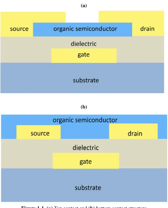
Figure 1-1. (a) Top contact and (b) Bottom contact structure
Figure 1-2. Pentacene molecular structure
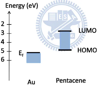
Figure 1-3. Energy scheme of the gold-pentacene interface
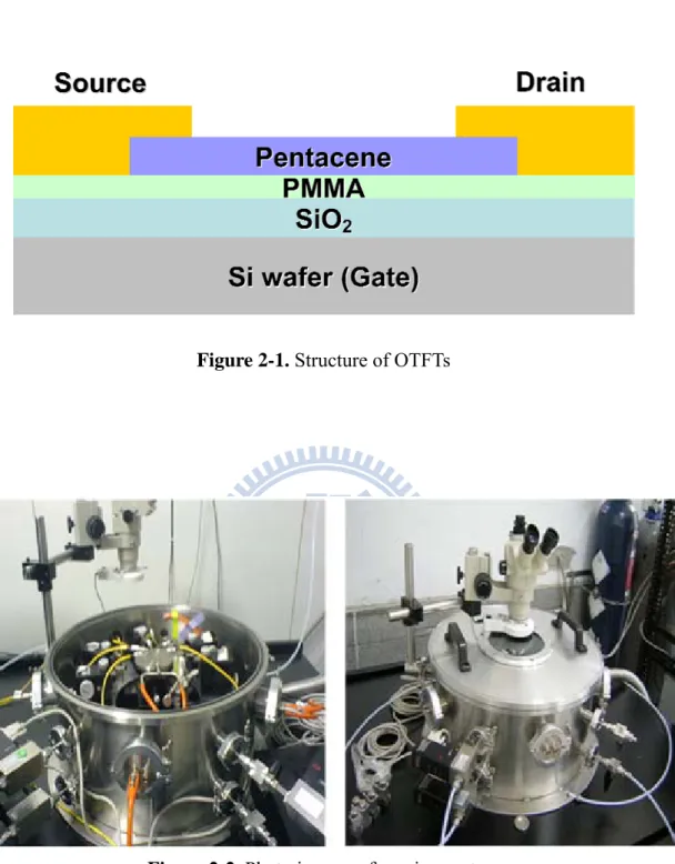
Figure 2-1. Structure of OTFTs
Figure 2-2. Photo images of sensing system
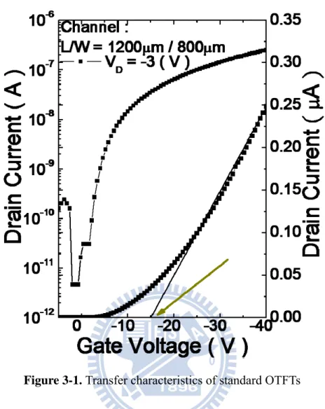
Figure 3-1. Transfer characteristics of standard OTFTs
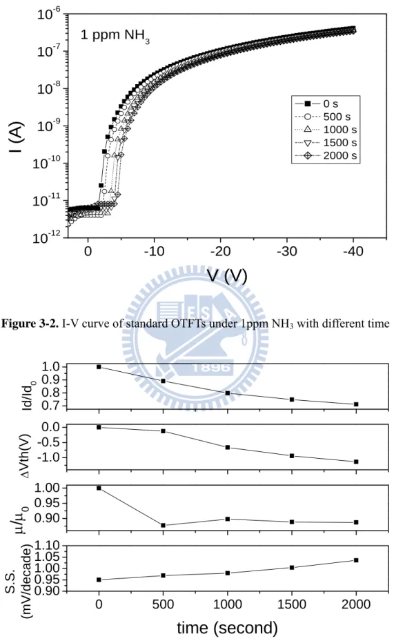
Figure 3-2. I-V curve of standard OTFTs under 1ppm NH3 with different time
Figure 3-3. The parameters variation of OTFTs under 1 ppm NH3 with different time
Figure 3-4. Illustration of scattering effect and traps for gas sensing
Figure 3-5. Illustration of screen effect for gas sensing
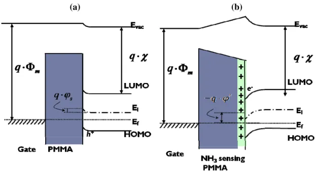
Figure 3-6. Energy band of (a) standard OTFTs and (b) Ammonia sensing PMMA OTFTs
Figure 3-7. (a) Threshold voltage shift and (b) mobility variation versus different ammonia concentration measured in 1000 seconds and 2000 seconds
Figure 3-8. Simulation of PMMA and UV-treated PMMA estimated by Gaussian 03 with ab initio calculation.
Figure 3-10. Energy band of (a) standard OTFTs and (b) UV-treated PMMA OTFTs
Figure 3-11. AFM images of pentacene film deposited on (a) PMMA and (b) UV-treated PMMA
Figure 3-12. (a) Threshold voltage shift (Vth) (b) mobility variation (/0) and (c)
drain current variation (I/I0) versus ammonia concentration in different waiting time
of standard OTFTs and UV-treated PMMA OTFTs
Figure 3-13. Threshold voltage shift (Vth) and mobility variation ((0-)/0)
percentage for standard and UV-treated OTFTs when devices were exposed to
different kinds of gas molecules.
Figure 3-14. Mobility variation versus different time of (a) standard OTFTs and (b) UV-treated PMMA OTFTs under different ammonia concentration from 0 second to
3000 seconds
Figure 3-15. Threshold voltage shift versus different time of (a) standard OTFTs and
(b) UV-treated PMMA OTFTs under different ammonia concentration
Figure 3-16. Threshold voltage shift versus different NH3 concentrations in the dry
ambient (RH=0%) and in the wet ambient (RH=50%) of (a) standard OTFTs and (b)
UV-treated PMMA OTFTs
Figure 3-17. (a) Mobility variation and (b) drain current variation versus different NH3 concentrations in the dry ambient (RH=0%) and in the wet ambient (RH=50%)
of standard OTFTs or UV-treated PMMA OTFTs
Table Captions
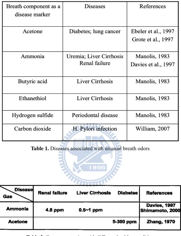
Table 1. Diseases associated with unusual breath odors
Table 2. Gas concentration with different healthy condition
Chapter 1
Introduction
1.1 Introduction of Organic Thin Film Transistors (OTFTs)
1.1.1 An Overview of Pentacene-Based Thin Film Transistors
Organic thin film transistors (OTFTs) based on conjugated polymers, oligomers,
or other molecules have received much attention for more than a decade. Efforts have
also been made to understand the material properties and device physics [1,2,3,4].
Compared to amorphous silicon device, OTFTs have advantages for the low cost,
flexibility, low-temperature, and large area processing, etc. Despite the extensive
research efforts to discover better materials for the active layer of OTFTs, pentacene
is one of the most widely used small molecules for device applications due to its high
field effect mobility and easy film formation properties [1,5,6,7]. Recently,
pentacene-based thin-film transistors (TFTs) are developed for sensors, display
backplane and radio frequency identification devices [8,9,10]. Nevertheless, there are
still several issues to be considered before realizing the applications of pentacene
TFTs: threshold voltage hysteresis, gate voltage stress resistance and the environment-
or ultraviolet (UV) - induced degradation of the pentacene channel [11,12,13,14]. It
1.1.2 Device Structures
In general, OTFTs are made of three parts: an insulator, a thin film of organic
semiconducting material, and three electrodes. Two of the electrodes, the source and
the drain, are in direct contact with the semiconductor to apply a source-drain voltage
and measure the source-drain current that flows through the organic thin film. The
third electrode, the gate, is isolated from the semiconductor by the insulator to
modulate the magnitude of the source-drain current. Because most organic
semiconductors are fragile materials, the deposition of organic semiconductors on the
insulator is much easier than the converse. Thus, the majority of OTFTs are built with
the bottom-gate architecture, which is divided into two structures: top contact and
bottom contact, in Fig1-1. In the bottom contact structure, contacts are deposited on
the insulator. Thus, the contact resistance in bottom contact is higher than in top
contact.
1.1.3 Organic Semiconductor Material
Organic semiconductors are traditionally classified as polymers or small
molecules. In our study, we chose pentacene as the organic semiconductor material.
show in Fig1-2. It is the p-type material, because holes are easily to transport than
electrons. The principle can be illustrated with Fig1-3, the energy scheme of the
gold-pentacene interface [15]. HOMO presents highest occupied molecular orbital,
and LUMO presents lowest unoccupied molecular orbital. When a positive voltage is
applied to the gate, negative charges are induced in the source. However, the LUMO
level of pentacene is quite far from the Fermi level of gold. It is very hard for the
electrons to inject into the pentacene film. In contrast, when a negative voltage is
applied to the gate, positive charges are induced. Because the HOMO level of
pentacene is close to the Fermi level of gold, holes can easily inject into the
pentacene.
1.1.4 Operation mechanisms of OTFTs
The operation mechanisms of OTFTs are originated from MOSFET. Both OTFTs
and MOSFET have semiconductor layer, insulator layer, and three electrodes. But
traditional MOSFET are operated in the inversion mode, while the OTFTs are
operated in the accumulation mode. Since pentacene is a p-type semiconductor
material, holes are the major transport carriers than electrons. When a negative gate
voltage is applied, the energy band of the pentacene film bends upwards and causes
like a capacitor. Because the conductance of the channel is proportional to the charge,
it is also proportional to the gate voltage. If we apply a source-drain voltage, the
accumulated holes transport from source to drain and result in the source-drain
current.
The operation current of OTFTs can be divided into two regions: linear region
and saturation region. At low source-drain voltage, the current is proportional to both
the gate and drain voltages. When the drain voltage increases to approach the gate
voltage, there is a pinch off of the channel, and the channel current becomes
independent of the drain bias. So, we call it the saturation region.
1.2 Ammonia Sensor and Their Applications
1.2.1 Application of Ammonia Sensors
Ammonia is an importance compound for living system. It can be widely utilized
in many fields, such as chemical industries, fertilizer factories, refrigeration systems,
food processing, fire power plants, and medical diagnosis, etc. For applications above,
the concentration control of ammonia is very important. For example, in chemical
industries, ammonia concentration is related to the quality of fertilizers and frozen
foods. Additionally, ammonia concentration plays a role in medical diagnosis. Tab1 is
diseases. It shows that ammonia is a disease marker for the uremia, liver cirrhosis, and
renal failure. Tab2 is the gas concentration with different healthy condition. The
ammonia concentration is 1~5 ppm for renal failure and 0.5~1 ppm for liver cirrhosis.
The most common method we use for diagnosis is by examining the ammonia
concentration of the blood. Recently, developments of a non-invasive diagnostic
method have received considerable attention. If we can develop a non-invasive,
inexpensive, portable and disposable diagnostic device, patient’s breath can be easily
detect and traced by the gas sensor.
1.2.2 Different Types of Ammonia Sensors
(a) Metal-oxide gas sensors
Some well-known materials for ammonia gas sensing are ZnO [16], iridium
oxide [17], molybdenum oxide [18], polyaniline [19,20,21], polypyrrole [22], Au and
MoO3-modified WO3[23,24], Pt- and SiO2-doped SnO2[25], etc. When the device is
exposed to analytes, the gas removes some of the adsorbed oxygen and modulates the
height of the potential barriers, thus changing the conductivity and creating the sensor
signal. However, various ammonia sensors reported work at high temperature such as
350℃, but it is not convenient to sense at such high temperature. Despite of high
sensors remains limited.
(b) Catalytic ammonia sensors
Catalytic ammonia sensor is based on the catalytic reaction of a metal layer with
ammonia gas. The reaction will cause a change in electrode potential and the charge
carrier concentration which can be quantified by using a field effect device, like a
capacitor or a transistor [26,27]. The detection limit can be 1 ppm.
(c) Conducting polymer gas detectors
Conducting polymer ammonia gas detectors use polymer, like polypyrrole and
polyaniline, to react with ammonia. During the process, ammonia can reversibly
reduce the oxidized form of polymer. Because the reduction of the polymer film
causes a change in the conductivity of material, we can use it to make resistometric or
amperometric ammonia detection [28,29]. However, the irreversible reaction between
ammonia and the polymer causes the sensitivity of the sensor decrease when exposed
to ammonia. The detection limit is about 1 ppm.
(d) Optical gas analyzers
which uses coloration reaction of ammonia with phenol and hypochlorite in aqueous
solutions [30,31]. One drawback is the slow kinetics of the reaction. The detection
limit is about 5 uM of ammonia in water or 90 ppb. The second method is optical
absorption ammonia detection [32]. By using a laser and a spectrograph, we can get a
spectrum of the light influenced by the gas composition. Although the method is very
sensitive and selective for ammonia sensing, the equipment is very expensive and it is
not suitable for miniaturized ammonia sensors.
1.3 OTFTs Ammonia Gas Sensors
The research of OTFT sensors started in the late 1980s, just after the first OTFTs
was proposed. Such sensors offer the advantages of simple process, low fabrication
cost, remarkable response repeatability [33] and selectivity [34,35]. Because many
types of organic molecules exhibit sensing behavior based on their chemical
compositions, sensibility and selectivity can be pursued by choosing ad hoc
chemically or biologically functionalized semiconducting polymer active layers for
the use of OTFTs in compact sensing systems or in bio-chips [33,36,37,38]. In
addition, [36,39] provided evidences that the OFET sensor has better performance
than a similar resistor-type sensor in drift, sensitivity, signal-to-noise ratio, response
multi-parameter sensors [40]. By measuring the parameters of field-induced
conductivity, threshold voltage, and field-effect mobility, we can get a fingerprint of
each gas. It makes the transistors to be more selective than conventional
chemiresistors. Besides, the morphology of active layer plays an important role on the
sensibility of OTFT sensors. The device response increases when the grain size is
reduced [41]. The effect of a channel length comparable to the grains size has also
been observed. In order to lower the limit of detection, nanoscale organic transistors
have been explored [42].
So far, the active layer of OTFT sensors include substituted thiophene polymers,
oligomers, naphthalenes, copper-phthalocyanine, pentacene and others. These devices
were exposed to different analytes, such as alcohols, ketones, thiols, nitriles, ester and
ring compounds. However, it does not have much research of ammonia sensors with
OTFTs. Our studies of pentacene-based OTFTs applied on ammonia sensor were the
first.
1.4 Motivation
In order to develop a non-invasive, inexpensive, portable and disposable
diagnostic device, we use pentacene-based OTFT to act as ammonia sensor. It is very
parameters in different ammonia concentrations. Furthermore, to enhance the
response to ammonia gas, we try to modify the sensing surface to obtain different
functional groups which has strong interaction with ammonia gas. Besides, we need to
discuss the recovery phenomenon to know whether it can be reverse or not. The
(a)
(b)
Figure 1-2. Pentacene molecular structure
Table 1. Diseases associated with unusual breath odors
Table 2. Gas concentration with different healthy condition
William, 2007 H. Pylori infection Carbon dioxide Manolis, 1983 Periodontal disease Hydrogen sulfide Manolis, 1983 Liver Cirrhosis Ethanethiol Manolis, 1983 Liver Cirrhosis Butyric acid Manolis, 1983 Davies et al., 1997 Uremia; Liver Cirrhosis
Renal failure Ammonia
Ebeler et al., 1997 Grote et al., 1997 Diabetes; lung cancer
Acetone References Diseases Breath component as a disease marker William, 2007 H. Pylori infection Carbon dioxide Manolis, 1983 Periodontal disease Hydrogen sulfide Manolis, 1983 Liver Cirrhosis Ethanethiol Manolis, 1983 Liver Cirrhosis Butyric acid Manolis, 1983 Davies et al., 1997 Uremia; Liver Cirrhosis
Renal failure Ammonia
Ebeler et al., 1997 Grote et al., 1997 Diabetes; lung cancer
Acetone
References Diseases
Breath component as a disease marker
Chapter 2
Experiment Setup
2.1 Fabrication of Organic Thin-Film Transistors
We chose highly-doped p-type silicon wafers with 100 nm thick silicon oxide as
the substrate. The p-type silicon was used as gate electrode, and the silicon oxide
layer was used as gate insulator. After cleaned with 5min de-ionized water-5min
acetone-5min de-ionized water, the particles and the impurities on the substrate were
removed in order to avoid gate leakage which may cause instability [43].
Then, soluble poly(methyl methacrylate) (PMMA) was spun on the silicon
oxide layer by the spin coater to improve the electric performance and increase the
grain boundaries [44]. The PMMA was obtained from MicroChem. Corp. with a
molecular weight of 95000 and was dissolved in anisole at 10 wt %. The spin speed
was accelerated from 0 to 1000 rpm during the first 10 seconds and further increased
to 7500 rpm during the following 10 seconds. After kept as 7500 rpm for 40 seconds,
the spin speed was decreased from 7500 to 1000 in the following 10 seconds and
further decreased to 0 rpm during 10 seconds. After the process of spin coating, the
PMMA layer was annealed by hot plate with 90℃ for 30 minutes. The capacity of
were then exposed to UV-light, whose wavelength is 175~285 nm and the output
power is 40 mW, for 60 seconds to change the functional group of PMMA.
Following, the pentacene material obtained from Aldrich with 99.9% purity was
evaporated through a shadow mask on the UV treated and non-UV treated
PMMA/SiO2 dielectric layer as the active layer. The deposition was started at the
pressure around 3 10 torr and the temperature was kept at 20℃. The deposition
rate of 1000-Å-thick pentacene was 0.1 Å/sec at the first 100Å and was smoothly
increased to 0.5 Å/sec at the 200Å to the 1000Å. The deposition temperature, the
deposition pressure and the deposition rate are the important parameters to decide the
ordering quality of the organic film [45].
Finally, we used gold as the source and drain electrodes. Due to its similar work
function with pentacene, we can get better injection from gold to pentacene film.
Before gold deposition, we deposited 50-Å-thick nickel through a shadow mask on
the pentacene film as the adhesion layer. Then, we deposited 1000- Å-thick gold on
the samples. The width (W) and length (L) of the device’s channel were 800 μm and
2.2 Gas Sensing System
In this study, we used OTFTs devices to sense five different kinds of gas as
following: ammonia (NH3), methane (CH4), acetone (CH3COCH3), alcohol (C2H5OH)
and carbon dioxide (CO2). To control the environment in the precise condition, we
measured the devices with a semiconductor analyzer (Keithley 4200-SCS) in a sealed
chamber. The inside volume of the chamber is about 42 L and its configuration image
is shown in Fig2-2. After putting the device into the chamber, we vacuumed it to the
pressure of 10 torr and then purged it with high purity nitrogen (99.99% N2) to the
pressure of 1 atm. This process can avoid the influence of moisture and other gases
we did not want to sense. Thus, the data measured in the N2 ambiance was the
standard data. Then, we injected the gas we wanted into the chamber and measured
the device’s characteristic.
The concentration of NH3 was controlled as 0.5, 1, 3 and 5 ppm (mg/L) by a
mass flow controller (MFC). CH4 and CO2 gases were also injected through a MFC
and their concentrations were controlled as 2 ppm. To get CH3COCH3 and C2H5OH
gases, we used a Tedlar bag and put liquid CH3COCH3 and C2H5OH inside. After
liquid CH3COCH3 and C2H5OH evaporated to saturate pressure, we injected the gases
into the chamber with a syringe which can control the concentration as more than 2
To discuss the influence of moisture during the gas sensing process, we also
provided different relative humidity (RH) environment. By using a N2 flow to pump
water, water vapor can be introduced into the chamber. We controlled the RH value as
0% and 50% with different input time and measured the RH with a hygrometer.
2.3 Parameter Extraction
It is also important to analyze the data with a good method. In this section, I introduce
the method we used to extract the three important parameters of the devices from the
electrical characteristics: field effect mobility, threshold voltage, and subthreshold
swing.
2.3.1 Field Effect Mobility
Field effect mobility is an important parameter because it is directly related to the
orientation of the active layer. When other molecular transports into the bulk of the
active layer, the orientation of the active layer will be influenced and the field effect
mobility will also be changed. Because the characteristics of pentacene-based thin
film transistors are similar to conventional MOSFETs, we used the same method to
D OX t cons V G D m V L WC V I g D tan ( ) m o x D g w C V L
, where W is the width, L is the length of the channel, and Cox is the capacitance of
the dielectric layer.
2.3.2 Threshold Voltage
Threshold voltage is also an important parameter because it strongly dependents on
dielectric surface states. When the device was exposed to a gas, which might create
charge sites on the dielectric surface, the threshold voltage shifted. With the drain
current in the linear region:
2
which can be simplify for VD VG VT to
(1)
, we extracted the threshold voltage by finding out the intersection point of the drain
2.3.3 Subthreshold Swing
Subthreshold swing represents how rapidly the device turn on from the off state. It is
related to the interface quality and the defect density of the device. We extract
subthreshold swing with
log
constant
D V D GI
V
SFigure 2-1. Structure of OTFTs
Chapter 3
Result and Discussion
In this chapter, we first discussed the gas-sensing phenomenon of standard OTFTs.
Then, we introduced the UV-treated PMMA method to improve the sensitivity of
OTFTs. Besides, we also discussed the selectivity and the phenomenon of recovery.
Finally, we increased the relative humidity to find out the environment influence of
the water.
3.1 Ammonia-sensing Phenomenon of Standard OTFTs
3.1.1 Electrical Properties of Standard OTFTs
Before exposing the device on the analytic gas, we measured the electrical
characteristics of the device at constant drain bias, V 3 V, and sweeping gate
bias from 5 V to -40 V. With the Fig3-1, we can extract the threshold voltage as -16.4
V, the mobility as 0.3 cm2/Vs, and subthreshold swing as 0.66 V/decade. Those data
was taken as standard one to be compared with other data under gas-sensing.
3.1.2 Gas Diffusion Model
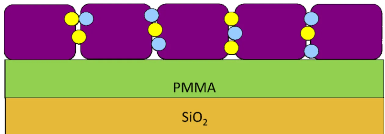
shown in Fig3-3, the variations of the turn-on current, field-effect mobility, and
threshold voltage shift were decreaed while the subthreshold swing was increased.
The turn-on current variation (Id/Id0), according to Eq(1), is affected by both threshold
voltage shift (Vth) and mobility variation (/0), where Id0 and 0 are the initial drain
current and the initial field-effect mobility.
The reason for the decreasing of mobility and threshold voltage is still not very
clear. A possible reason is that positive ammonia ions (NH4+) or polar ammonia
molecular (NH3) penetrated through the grain boundaries into the bulk of pentacene
layer and created scattering centers or traps [47], as Fig3-4. In addition, the polar
molecules may decrease the rate of charge transport in organic materials by increasing
the energetic disorder through charge–dipole interactions [48]. Because the
concentration of ammonia was fixed, the mobility decreased to saturate very soon.
On the other hand, the threshold voltage was decreased gradually. The reason
may be the hole-traps, which were attributed to the NH3 or NH4+ near dielectric
interface and caused lower concentration of gate-induced mobile carriers [49], as
Fig3-5. Therefore, it needs more negative gate voltage to induce holes in the
p-channel, as Fig3-6 Because it needed more time for the formation of the hole-traps
near the interface between pentacene and dielectric layer, the threshold voltage shift
conformed that the density of interface traps between pentacene and dielectric layer
were increased [46].
3.1.3 Ammonia Concentration Effect
To confirm the gas sensing model, we exposed the devices to different ammonia
concentration from 0.5ppm to 5ppm. Fig3-7 (a)(b) shows the threshold voltage shift
and mobility variation versus different ammonia concentration measured in different
time (1000 seconds and 2000 seconds).It clearly shows that the threshold voltage shift
and mobility variation were increased with the increasing of ammonia concentration,
which caused more NH4+ or NH3 penetrate through the grain boundaries of pentacene
film. We can also find that after waiting for 2000 seconds, the threshold voltage shift
more than waiting for 1000 seconds. However, the mobility variation did not change
much between 2000 seconds and 1000 seconds waiting time. The phenomenon
conformed to the gas sensing model we mentioned above.
For application to non-invasive diagnostic sensor for cirrhotic patients, it is
necessary to monitor ammonia concentration at 0.5 ppm or lower so that the breath
samples between healthy person (breath ammonia level: 0.278 ppm) and a patient
(breath ammonia level: 0.745 ppm) can be distinguished [50]. For the patients with
(dangerous) [51]. However, it was hard to distinguish the variation difference
between 0.5 ppm and 1 ppm ammonia with the standard OTFTs. Thus, we needed to
find another way to improve the sensing ability.
3.2 Ammonia-sensing Phenomenon of UV-treated PMMA
OTFTs
To enhance the sensitivity, we used a UV-light irradiation on PMMA to modify
the dipole moment of the dielectric surface [52]. The PMMA functional end-groups
changed from −COOCH3 to −COOOH, which will result in the negative charge sites
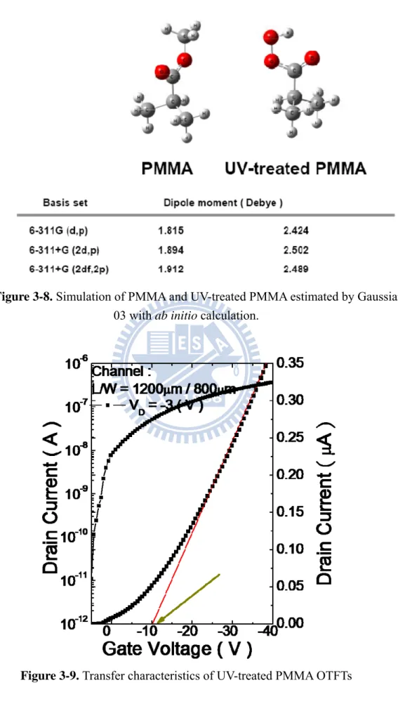
near the PMMA surface. Fig3-8 is the simulation of PMMA and UV-treated PMMA
which were estimated by Gaussian 03 with ab initio calculation. The dipole moment
of standard PMMA and UV-treated PMMA were 1.81~1.91 Debye and 2.42~2.5
Debye, respectively.
3.2.1 Electrical Properties of UV-treated PMMA OTFTs
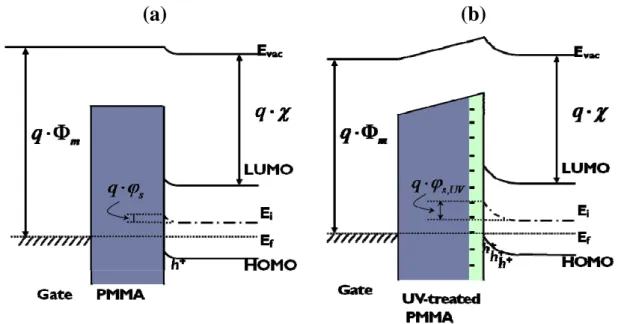
Fig3-9 is the I-V curve of UV-treated device which was measured at constant
drain bias, V 3 V, and sweeping gate bias from 5 V to -40 V. The threshold
voltage we extracted is -11.1 V, mobility is 0.31 cm2/Vs, and subthreshold swing is
turn on and its subthreshold swing was larger. It may due to the change of functional
end-groups (from –CH3 to –COOOH) produced by UV-treatment on PMMA surface,
which will result in the negative charged-states near PMMA surface. With the
comparing of the energy band of standard OTFTs Fig3-10(a) and UV-treated PMMA
OTFTs Fig3-10(b), the negative charge sites, which produced by UV treatment,
caused a surface potential change that induced a bending of the HOMO level at the
interface and increased the carrier density in the channel [53,54,55,56,57]. Thus, it did
not need so much negative gate voltage to induce holes for turn-on. However, the
mobility of both devices was the same. It indicated that the structure of the pentacene
film was not affected by UV treatment. Fig3-11 (a)(b) are the AFM images of
pentacene film deposited on PMMA and UV-treated PMMA, respectively. We can
find that the grains and roughness were almost the same.
To verify the hypothesis, we calculated the number of interface states Nss with
the equation [59],
. . log( )
[
1]
/
total SSC
S S
e
N
kT q
q
where S.S. is the subthreshold swing, e is the Napierian logarithm, k is the
is the absolute temperature.
For standard OTFTs (subthreshold swing = 0.64 V/decade), the number of interface
states were 1.431012 cm-2eV-1; for UV-treated OTFTs (subthreshold swing = 0.68
V/decade), the number of interface states were 1.531012 cm-2eV-1. It was reasonable
to observe that UV-treated device exhibited higher interface state density than that of
standard device.
3.2.2 Sensing Phenomenon of UV-treated PMMA OTFT
We measured the UV-treated PMMA devices at the same condition as standard
devices. After extracting the parameters from I-V curve, we found that the threshold
voltage shifted much, the mobility and drain current also decreased much compared
with standard OTFTs. Fig3-12(a)(b)(c) are the threshold voltage shift, mobility
variation and drain current versus ammonia concentration in different waiting time of
standard OTFTs and UV-treated PMMA OTFTs, respectively. We proposed that UV
radiation increased the dipole moment of dielectric surface and attracted ammonia gas
molecules to accumulate near the dielectric surface. Also, the negative charge sites
which caused by UV treatment enhanced the attraction of positive ammonia ions
standard OTFTs. The variation difference between 0.5 ppm and 1 ppm ammonia can
be large enough to be distinguished. Therefore, UV treatment can enhance the
ammonia sensitivity.
3.3 Selectivity of Gas Sensing
To research and design an ammonia gas sensor, it is very important to confirm
the sensing selectivity. Thus, we exposed the devices to five different kinds of gas that
may exist in human’s breath, including ammonia (1 ppm), methane (2 ppm), acetone
(more than 1 ppm), alcohol (more than 1 ppm) and carbon dioxide (1000 ppm). With
Fig3-13, we can find that at a fixed sensing time (2000 sec), the threshold voltage
shift was not distinct with increased time under the condition of methane (CH4),
acetone (CH3COCH3), alcohol (C2H5OH) and carbon dioxide (CO2). Although the
concentration of ammonia was the lowest, the threshold voltage shift was evident
after 1000 seconds. The variation of mobility under ammonia environment was also
the biggest. With the sensing index, threshold voltage shift and mobility variation, we
can confirm that both standard and UV-treated OTFTs exhibited good selectivity
3.4 Phenomenon of Recovery
In order to verify the sensing mechanism, we discuss the phenomenon of
recovery. At 0 second, both the standard and UV-treated devices were exposed to
nitrogen. Then, during 0 to 3000 seconds, the devices were exposed to 0 ppm
(nitrogen), 1 ppm, 3 ppm, 5ppm ammonia gas individually. After that, during 3000 to
4500 seconds, the ambience was purged with nitrogen.
With Fig3-14 (a)(b), we can find that the mobility of both the standard device
and UV-treated PMMA device had recovery. Although the value could not recover to
the beginning, the phenomenon were immediately when the ammonia was purged out.
The recovery of mobility may due to the decreasing of ammonia which may create
scattering centers or traps[47].
However, with Fig3-15 (a)(b), the threshold voltage shift of both devices did not
have evident recovery. Although the slope of threshold voltage shift was gradual when
the ammonia was purged out, the value could not be increased. The reason may be
that the ammonia molecular NH3 or ammonia ions NH4+ had been trapped on the
interface of the dielectric and pentacene layer. Thus, the reaction could not be
3.5 Influences of Environment Humidity
In order to know the influence of humidity to the sensing model, we changed the
measure environment by increasing the relative humidity (RH) in the chamber. In the
wet nitrogen ambient (RH=50%), comparing with dry nitrogen ambient (RH=0%), we
can find that the threshold voltage of standard device had a negative shift, as
Fig3-16(a). However, in the same condition, the UV-treated PMMA device had a
positive threshold voltage shift, Fig3-16(b). It may due to different functional-end
group of dielectric. The polar -COOOH functional-end group of UV-treated PMMA
can interact with water molecules and create acceptor-like traps [60]. Because extra
holes were induced by trapped electrons, the threshold voltage turned positive [58].
Nevertheless, it is hard for less-polar -COCH3 functional-end group of standard
devices to interact with water molecules. When the polar water molecules diffused
into the interface between dielectric and pentacene layer, it may attribute hole-traps
near dielectric interface and caused lower concentration of gate-induced mobile
carriers. Therefore, it needs more negative gate voltage to induce holes in the
p-channel.
With the increasing of ammonia concentration, both the standard device and
UV-treated PMMA device had negative threshold voltage shift, especially in the wet
opposite for the UV-treated PMMA device, we can confirm that something must
happen in the wet ammonia ambient. The chemical reaction between water and
ammonia,
H O
NH
NH
OH
, may be enhanced due to the increased H2O, which resulted in more NH4+ and less
H2O. Thus, the threshold voltage shifted much to the negative side in wet ammonia
ambient.
From Fig3-17(a), we can find that the mobility variations of both standard
devices and UV-treated PMMA device were decreased more in wet ambient than in
dry ambient. The reduction of carrier mobility was because polar water molecules
residing at grain boundaries interact with carriers [61]. Scattering effect or the field
screening effect may be the mechanism to describe interactions between polar water
molecules and carriers [62]. Because UV-treated PMMA devices have polar surface
which can attract more dipole water, the decreased difference between wet and dry
ambient of UV-treated PMMA devices were more than standard devices.
For the UV-treated PMMA devices, since threshold voltage moved to positive
value in wet nitrogen ambient, there should be an increase of the drain current
variation. However, from Fig3-17(b), the drain current variation of UV- treated device
attributed to a reduction of mobility [58]. But, we can see the influence of threshold
voltage in the difference of decreased current between wet and dry ambient, the
Figure 3-2. I-V curve of standard OTFTs under 1ppm NH3 with different time
Figure 3-3. The parameters variation of OTFTs under 1 ppm NH3 with different time
0 -10 -20 -30 -40 10-12 10-11 10-10 10-9 10-8 10-7 10-6 1 ppm NH 3
I (A
)
V (V)
0 s 500 s 1000 s 1500 s 2000 s 0 500 1000 1500 2000 0.90 0.95 1.00 1.05 1.10 0.90 0.95 1.00 -1.0 -0.5 0.0 0.7 0.8 0.9 1.0 S.S. (m V/decade)time (second)
/
0 Vth(V) Id/Id 0Figure 3-4. Illustration of scattering effect and traps for gas sensing
(a) (b)
Figure 3-6. Energy band of (a) standard OTFTs and (b) Ammonia sensing PMMA OTFTs
(a) (b)
Figure 3-7. (a) Threshold voltage shift and (b) mobility variation versus different ammonia concentration measured in 1000 seconds and 2000 seconds
0 1 2 3 4 5 -5 -4 -3 -2 -1 0 1 Standard Vt h (V) NH 3 concentration (ppm) 0 second 1000 seconds 2000 seconds 0 1 2 3 4 5 0.00 0.25 0.50 0.75 1.00 1.25 Standard / 0 NH 3 concentration (ppm) 0 second 1000 seconds 2000 seconds
Figure 3-8. Simulation of PMMA and UV-treated PMMA estimated by Gaussian 03 with ab initio calculation.
(a) (b)
(a)
(b)
Figure 3-11. AFM images of pentacene film deposited on (a) PMMA and (b) UV-treated PMMA
(a)
(b)
0 1 2 3 4 5 -5 -4 -3 -2 -1 0 1Standard
Vth ( V ) NH3 concentration (ppm) 0 (second) 1000 (second) 2000 (second) 0 1 2 3 4 5 -5 -4 -3 -2 -1 0 1UV-treated
V th (V ) NH3 concentration (ppm) 0 (second) 1000 (second) 2000 (second) 0 1 2 3 4 5 0.00 0.25 0.50 0.75 1.00 1.25Standard
NH 3 concentration (ppm) 0 (second) 1000 (second) 2000 (second) 0 1 2 3 4 5 0.00 0.25 0.50 0.75 1.00 1.25UV-treated
NH3 concentration (ppm) 0 (second) 1000 (second) 2000 (second)(c)
Figure 3-12. (a) Threshold voltage shift (Vth) (b) mobility variation (/0) and
(c) drain current variation (I/I0) versus ammonia concentration in different waiting
time of standard OTFTs and UV-treated PMMA OTFTs
0 1 2 3 4 5 0.00 0.25 0.50 0.75 1.00 1.25
Standard
Id/I d0 NH3 concentration (ppm) 0 (second) 1000 (second) 2000 (second) 0 1 2 3 4 5 0.00 0.25 0.50 0.75 1.00 1.25UV-treated
Id/Id0 NH3 concentration (ppm) 0 (second) 1000 (second) 2000 (second)Figure 3-13. Threshold voltage shift (Vth) and mobility variation ((0-)/0)
percentage for standard and UV-treated OTFTs when devices were exposed to different kinds of gas molecules.
(a) (b)
0
1
2
CH4 CH3COCH3 C2H5OH CO2 NH3|
V
th(V
)|
Standard Devices UV-treated Devices N20
5
10
15
20
25
(
-
)
/
(%
)
Standard Devices UV-treated Devices CH4 CH3COCH3 C2H5OH CO2 NH3 N2Figure 3-14. Mobility variation versus different time of (a) standard OTFTs and (b) UV-treated PMMA OTFTs under different ammonia concentration from 0
second to 3000 seconds
(a) (b)
Figure 3-15. Threshold voltage shift versus different time of (a) standard OTFTs and (b) UV-treated PMMA OTFTs under different ammonia concentration
0 1500 3000 4500 0.4 0.5 0.6 0.7 0.8 0.9 1.0
Standard
/ 0 time (second) 0.5 ppm NH3 1 ppm NH3 3 ppm NH3 5 ppm NH3 0 1500 3000 4500 0.4 0.5 0.6 0.7 0.8 0.9 1.0UV-treated
/ 0 time (second) 0 1500 3000 4500 -5 -4 -3 -2 -1 0Standard
Vth ( V ) time (second) 0.5 ppm NH3 1 ppm NH3 3 ppm NH3 5 ppm NH3 0 1500 3000 4500 -5 -4 -3 -2 -1 0UV-treated
Vth ( V ) time (second)(a) (b)
Figure 3-16. Threshold voltage shift versus different NH3 concentrations in the dry
ambient (RH=0%) and in the wet ambient (RH=50%) of (a) standard OTFTs and (b) UV-treated PMMA OTFTs
0 1 2 3 4 5 -7 -6 -5 -4 -3 -2 -1 0 1
Standard
Vth ( V ) NH3 concentration (ppm) RH = 0% RH = 50% 0 1 2 3 4 5 -7 -6 -5 -4 -3 -2 -1 0 1 Vth (V) NH 3 concentration (ppm) RH = 0% RH = 50%UV-treated
(a)
(b)
Figure 3-17. (a) Mobility variation and (b) drain current variation versus different NH3 concentrations in the dry ambient (RH=0%) and in the wet ambient
(RH=50%) of standard OTFTs or UV-treated PMMA OTFTs
0 1 2 3 4 5 0.00 0.25 0.50 0.75 1.00 1.25
Standard
NH3 concentration (ppm) RH = 0% RH = 50% 0 1 2 3 4 5 0.00 0.25 0.50 0.75 1.00 1.25Standard
Id /I d0 NH3 concentration (ppm) RH = 0% RH = 50% 0 1 2 3 4 5 0.00 0.25 0.50 0.75 1.00 1.25UV-treated
NH 3 concentration (ppm) RH = 0% RH = 50% 0 1 2 3 4 5 0.00 0.25 0.50 0.75 1.00 1.25UV-treated
Id /Id 0 NH 3 concentration (ppm) RH = 0% RH = 50%Chapter 4
Conclusion
A pentacene-based OTFT was shown to be highly sensitive for ammonia sensing
from 0.5 to 5 ppm, a critical range for the diagnosis of patients with chronic liver
diseases and renal failure. This demonstrated that OTFT devices, which can be
fabricated by simple and cheap process and exhibited channel length and width as
large as several hundreds of microns, are useful as non-invasive biomedical sensors.
This is on the contrary to inorganic MOSFET devices that require high fabrication
cost and complicated fabrication process to scale down its dimension to the range of
nanometers to increase the gas sensing sensitivity. The sensitivity and selectivity of
OTFTs as gas sensor can be further improved by the modification of the PMMA
dielectric layer, selecting suitable measuring parameters and providing additional
local electric field. Due to the simple fabrication processes of the devices, OTFTs are
Reference
[1] Y. Y. Lin, D. J. Gundlach, S. F. Nelson, and T. N. Jackson, IEEE Trans. Electron
Devices 44, 1325 (1997)
[2] G. Horowitz, M. E. Hajlaoui, and R. Hajlaoui, J. Appl. Phys. 87, 4456 (2000)
[3] D. Knipp, R. A. Street, A. Volkel, and J. Ho, J. Appl. Phys. 93, 347 (2003)
[4] A. Volkel, R. A. Street, and D. Knipp, Phys. Rev. B 66, 195336 (2002)
[5] G. Horowitz, Adv. Mater. (Weinheim, Ger.) 10, 365 (1998)
[6] H. E. Katz and Z. Bao, J. Phys. Chem. B 104, 671 (2000)
[7] C. D. Dimitrakopoulos, S. Purushothanman, J. Kymissis, A. Callegari, and J. M.
Shaw, Science 283, 822 (1999)
[8] I. Manunza, A. Sulis, and A. Bonfiglio, Appl. Phys. Lett. 89. 143502 (2006)
[9] K. Nomoto, N. Hirai, N. Yoneya, N. Kawashima, M. Noda, M. Wada, and J.
Kasahara, IEEE trans. Electron Devices 52, 1519 (2005)
[10] R. Rotzoll, S. Mohapatra, V. Olariu, R. Wenz, M. Grigas, K. Dimmler, O.
Shchekin, and A. Dodabalapur, Appl. Phys. Lett. 88, 123502 (2006)
[11] Y. H. Noh, S. Y. Park, S,-M. Seo, and H. H. Lee, Org. Electron, 7, 271 (2006)
[12] D. K. Hwang, J. H. Park, J. Lee, J.-M. Choi, J. H. Kim, E. Kim, and S. Im, J.
[13] C. R. Kagan, A. Afzali, and T. O. Graham, Appl. Phys. Lett. 86, 193505 (2005)
[14] W. J. Kim, W. H. Koo, S. J. Jo, C. S. Kim, H. K. Baik, D. K. Hwang, K. Lee, J. H.
Kim, and S. Im, Electrochem. Solid-state Lett. 9, G251 (2006)
[15] A. Kahn, N. Koch, W. Gao, J. Polym. Sci. B, Polym. Phys. 41, 2529-2548 (2003)
[16] G. S. Trivikrama Rao, and D. Tarakarama Rao, Sens. Actuators B 55, 166-169
(1999)
[17] A. Karthigeyan, R. P. Gupta, K. Scharnagl, M. Burgmair, S. K. Sharma, I. Eisele,
Sens. Actuators B 85, 145-153 (2002)
[18] D. Mutschall, K. Holzner, E. Obermeier, Sens. Actuators B 36, 320-324 (1996)
[19] K. P. Kakde, D. J. Shirale, H. J. Kharat, P. D. Gaikwad, P. A. Savale, V. K. Gade,
M. D. Shirsat, Proceedings of NSPTS-11, C 17 1-5 (2006)
[20] A. L. Kukla, Y. M. Shirshov, S. A. Piletsky, Sens. Actuators B 37, 135-140 (1996)
[21] V. V. Chabukswar, S. Pethkar, A. A. Athawale, Sens. Actuators B 77, 657-663
(2001)
[22] G. Lahdesmaki, A. Lewenstam, A. Ivaska, Talanta 43, 125-134 (1996)
[23] X. Wang, N. Miura, N. Yamazoe, Sens. Actuators B 66, 74-76 (2000)
[24] C. N. Xu, N. Miura, Y. Ishida, K. Matuda, N. Yamazoe, Sens. Actuators B 65,
163-165 (2000)
[26] F. Winquist, A. Spetz, I. Lundstrom, Anal. Chim. Acta 164, 127-138 (1984)
[27] I. Lundstrom, A. Spetz, F. Winquist, U. Ackelid, H. Sundgren, Sens. Actuators B
1 (1-6),15-20 (1990)
[28] E. Palmqvist, C. Berggren Kriz, K. Svanberg, M. Khayyami, D. Kriz, Biosens.
Bioelectron. 10, 283-287 (1995)
[29] I. Lahdesmaki, A. Lewenstam, A. Ivaska, Talanta 43, 125-134 (1996)
[30] M. P. E. Berthelot, Repertoire Chimique Appliqueel 284 (1859)
[31] P. L. Saerle, Analyst 109, 549-568 (1984)
[32] G. H. Mount, B. Rumberg, J. Havig, B. Lamb, H. Westberg, D. Yonge, K. Johson,
R. Kincaid, Atmos. Environ. 36 (11), 1799-1810 (2002)
[33] B. Crone, A. Dodabalapur, A. Gelperin, L. Torsi, H. E. Katz, A. J. Lovinger, Z.
Bao, Appl. Phys. Lett. 78, 2229-2231 (2001)
[34] M. C. Tanese, L. Torsi, N. Cioffi, D. Colangiuli, G. M. Farinola, F. Babudri, F.
Naso, M. M. Giangregorio, L. A. Zotti, L. Sabbatini, P. G. Zambonin, Sens. Actuators
B 100, 17-21 (2004)
[35] D. Fine, D. Cauble, T. Jung, H. von Seggern, M. Krische, A. Dodabalapur, APS
Meeting (2003)
[36] T. Someya, H. E. Katz, A. Gelperin, A. J. Lovinger, A. Dodabalapur, Appl. Phys.
[37] L. Torsi, M. C. Tanese, N. Cioffi, M. C. Gallazzi, L. Sabbatini, P. G. Zambonin,
G. Raos, S. V. Meille, M. M. Giangregorio, J. Phys. Chem. B 107, 7589-7594 (2003)
[38] Z. –T. Zhu, J. T. Mason, R. Diechkermann, G. Malliaras, Appl. Phys. Lett. 81,
4643-4645 (2002)
[39] T. Someya, T. Sekitani, S. Iba, Y. Kato, H. Kawaguchi, T. Sakurai, Proc. Natl. Sci.
USA 101, 9966-9970 (2004)
[40] L. Torsi, A. Dodabalapur, L. Sabbatini, P. G. Zambonin, Sens. Actuators B 67,
312-316 (2000)
[41] L. Torsi, A. J. Lovinger, B. Crone, T. Someya, A. Dodabalapur, H. E. Katz, A.
Gelperin, J. Phys. Chem. B 106, 12.563-12.568 (2002)
[42] L. Wang, D. Fine, A. Dodabalapur, Appl. Phys. Lett. 85 (26), 6386-6388 (2004)
[43] M. J. Powell, Appl. Phys. Lett. 43, 597-599 (1983)
[44] H. L. Cheng, Y. S. Mai, W. Y. Chou, and L. R. Chang, Appl. Phys. Lett. 90,
171926 (2007)
[45] C. D. Dimitrakopoulos, A. R. Brown, A. Pomp, J. Appl. Phys. 80, 2501 (1996).
[46] L. Takeya, T. Nishikawa, T. Takenobu, S. Kobayashi, Y. Iwaea, T. Mitani, Appl.
Phys. Lett. 85, 5078 (2004)
[47] D. J. Gundlach, T. N. Jackson, D. G. Schlon, and S. F. Nelson, Appl. Phys.
[48] S. V. Novikov, D. H.Dunlap, V. M. Kenkre, P. E. Parris, and A. V. Vannikov, Phys.
Rev. Lett. 81, 4472 (1998)
[49] K. P. Pernstich, S. Haas, D. Oberhoff, C. Goldmann, D. J. Gundlach, B. Batlogg,
A. N. Rashid, and G. Schitter, J. Appl. Phys. 96. 11 (2004)
[50] C. Shimamoto, I. Hirata, and K. Katsu, Hepato-Gastroenteral, 47, 443 (2000)
[51] A. Manolis, Clin. Chem. 29, 5 (1983)
[52] H. W. Zan and K. H. Yen, Electrochem. Solid-state Lett. 118 H222-H225 (2008)
[53] A. Bolognesi, M. Berliocchi, M. Manenti, A. D. Carlo, P. Lugli, K. Lmimouni, C.
Dufour, IEEE Trans. Electron Device 51, 1997 (2004)
[54] S. Scheinert, G. Paasch, M. Schrodner, H. -K. Roth, S. Sensfuss, Th. Doll, J.
Appl. Phys. 92, 330 (2002)
[55] K. P. Pernstich, S. Haas, D. Oberhoff, C. Goldmann, D. J. Gundlach, B. Batlogg,
A. N. Rashid, G. Schitter, J. Appl. Phys. 96, 6431 (2004)
[56] J. Takeya, T. Nishikawa, T. Takenobu, S. Kobayashi, Y. Iwasa, T. Mitani, C.
Goldmann, C. Krellner, B. Batlogg, Appl. Phys. Lett. 85, 5078 (2004)
[57] Y. S. Yang, S. H. Kim, S. C. Lim, J. -I. Lee, J. H. Lee, L. -M. Do, T. Zyung, Appl.
Phys. Lett. 83, 3939 (2003)
[58] D. Li, E. J. Borkent, R. Nortrup, H. Moon, H. Katz, and Z. Bao, Appl. Phys. Lett.
[59] K. N. U. Narayanan, D. S. Sylvie, J. M. Nunzi, J. Phys. D: Appl. Phys. 38, 1148
(2005)
[60] S. H. Kim, H. Yang, S. Y. Yang, K. Hong, D. Choi, C. Yang, D. S. Chung, and C.
E. Park, Organic electronics 9, 673-677 (2008)
[61] D. H. Dunlap, P. E. Parris, and V. M. Kenkre, Phys. Rev. Lett. 77, 542 (1996)