This content has been downloaded from IOPscience. Please scroll down to see the full text.
Download details:
IP Address: 140.113.38.11
This content was downloaded on 25/04/2014 at 03:17
Please note that terms and conditions apply.
Site-controlled self-assembled InAs quantum dots grown on GaAs substrates
View the table of contents for this issue, or go to the journal homepage for more 2010 Nanotechnology 21 295304
(http://iopscience.iop.org/0957-4484/21/29/295304)
Nanotechnology 21 (2010) 295304 (4pp) doi:10.1088/0957-4484/21/29/295304
Site-controlled self-assembled InAs
quantum dots grown on GaAs substrates
Shih-Yen Lin
1,2,3, Chi-Che Tseng
1, Tung-Hsun Chung
1,
Wen-Hsuan Liao
1, Shu-Han Chen
1and Jen-Inn Chyi
1,41Research Center for Applied Sciences, Academia Sinica, Taipei 11529, Taiwan 2Department of Photonics, National Chiao-Tung University, Hsinchu 30010, Taiwan 3Institute of Optoelectronic Sciences, National Taiwan Ocean University, Keelung 20224,
Taiwan
4Department of Electrical Engineering, National Central University, Jhongli, 32001, Taiwan
E-mail:[email protected]
Received 15 April 2010, in final form 25 May 2010 Published 5 July 2010
Online atstacks.iop.org/Nano/21/295304
Abstract
Atomically-flat surfaces are obtained after thin GaAsSb buffer layer growth on GaAs substrates with regular-distributed nano-holes formed after oxide desorption of the local
atomic-force-microscopy anode oxidation. Different from the samples with GaAsSb buffer layers, increasing surface root-mean-square roughness is observed for the GaAs-buffered samples with increasing GaAs buffer layer thickness. The phenomenon is attributed to the enhanced adatom migration resulting from the incorporation of Sb atoms. By using the substrates with nano-holes after buffer layer growth, site-controlled self-assembled InAs quantum dots (QDs) are observed with the deposition of a below-critical-thickness InAs coverage of 1.3 monolayer (ML).
(Some figures in this article are in colour only in the electronic version)
1. Introduction
A lot of effort has been devoted to the fabrication and device applications of self-assembled quantum-dot (QD) structures in recent years [1–4]. Although defect-free QDs could be easily obtained by molecular beam epitaxy (MBE) in the Stranski–Krastanov (SK) growth mode, position control of each individual QD is always very difficult for this kind of growth mode. To achieve the goal of site-controlled QDs, nano-patterning is always required to localize the In adatom migration such that preferential growth positions would be observed for the self-assembled QDs. Among all the reports, in situ scanning tunneling microscope (STM)— assisted nanolithography has been proved to be one promising approach for this purpose [5–8]. With the multi-chamber system including MBE and STM systems, site-controlled QDs could be obtained by STM-induced nanolithography in the STM chamber and following QD growth in the MBE chamber. The major disadvantage of this approach would be the high cost and low throughput due to the involvement of ultra-high-vacuum systems. Ex situ approaches such as atomic-force microscope (AFM) tip induced nano-oxidation have also been
proposed [9, 10]. Although QD positioning could also be achieved via this approach, an additional atomic hydrogen source is required to remove the nano-oxides such that smooth GaAs surfaces can be obtained after buffer layer growth. The additional hydrogen source in the MBE chamber would complicate the fabrication procedure of the site-controlled QDs. Therefore, if traditional MBE growth procedures such as oxide thermal deoxidation, smooth surfaces after buffer layer growth and free In adatom migration can be adopted to achieve site-controlled self-assembled QDs, the fabrication of such samples could be greatly facilitated. To achieve this goal, alternative choices of buffer layers should be adopted.
In this paper, atomically-flat surfaces are obtained after thin GaAsSb buffer layer growth on GaAs substrates with regular-distributed nano-holes formed after thermal desorption in the MBE chamber of the local AFM anode oxidation. Since fully covering the holes is to be avoided, a thin buffer layer thickness on the order of several tens of nanometers is required. Compared with the GaAsSb-buffered samples, increasing surface root-mean-square (RMS) roughness is observed for the GaAs-buffered samples with increasing GaAs buffer layer thickness. The phenomenon is attributed to the enhanced
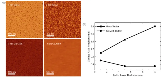
Nanotechnology 21 (2010) 295304 S-Y Lin et al 5 nm GaAsSb 1 nm GaAs 5 nm GaAs 600 nm 600 nm 600 nm 600 nm 1 nm GaAsSb 0 10 0.4 0.8 1.2 1.6 2.0 2.4
Buffer Layer Thickness (nm)
2 4 6 8 GaAs Buffer GaAsSb Buffer Surface RMS Roughness (nm) (a) (b)
Figure 1.(a) The AFM images of the un-patterned regions on the patterned GaAs substrates after 1 and 5 nm GaAs and GaAsSb buffer layer growth and (b) the surface RMS roughness values of the samples after 1, 5 and 10 nm GaAs/GaAsSb buffer layer growth.
adatom migration resulting from the incorporation of Sb atoms. After the GaAsSb buffer layer growth, the surface RMS roughness would remain the same with additional GaAs layer grown on the substrates. By using the substrates with nano-holes after buffer layer growth, site-controlled self-assembled InAs QDs are observed with the deposition of a below-critical-thickness InAs coverage of 1.3 monolayer.
2. Experiments
The AFM local oxidation is performed over (100) oriented semi-insulating GaAs substrates by using a Vecco Innova AFM system. Before performing AFM oxidation, the substrates are dipped in 1.5% NaOH solution and 3.7% HCl solution in sequence. After the procedure, oxides with a separation of 1 µm are prepared on the GaAs substrates by using AFM anode oxidation. The substrates are set to ground, and a negative bias −8 to −10 V is applied to the AFM tip in DC mode. The relative humidity of the atmosphere is kept at 50%. To investigate the influence of oxide size on the adatom migration after buffer layer growth, two sets of samples with average oxide height/diameter 4/150 and 7/180 nm are prepared. After oxidation, the samples are loaded into the MBE chamber. The growth procedure of the samples with GaAsSb buffer layers is as follows: (a) thermal desorption of the surface oxides at 620◦C for 7 min in an As2 background, (b) Sb irradiation on the surfaces at 580◦C
for 15 s in an Sb2/As2 background with the Sb/As beam equivalent pressure (BEP) ratio kept at 0.025 and (c) 1, 5, 10 nm GaAsSb buffer layer growth at 580◦C. For comparison, samples with 1, 5, 10 nm GaAs buffer layers are also grown at 580◦C. For the GaAs growth, the V/III ratio is kept at 31. The Sb composition of the GaAsSb buffer layer is 3%, as determined by high-resolution x-ray diffraction (HRXRD) measurements. The In effusion cell adopted is a standard double-filament effusion cell ABN 135 DF from Riber Corp.
The calibration of the InAs coverage is done by using an in
situ reflection high-electron diffraction system (RHEED) on an
un-patterned GaAs substrate. The transient InAs growth rate is obtained via the formula RInAs = 1.7 monolayer (ML)/(time
duration to observe a spotty RHEED pattern) [11]. The growth temperature for the InAs QDs is 510◦C. On the un-patterned substrate, when the below-critical-thickness 1.3 ML InAs is deposited, streaky RHEED patterns are still observed, which means that under normal growth conditions, no InAs QDs would be observed with 1.3 ML InAs coverage. To investigate the surface morphologies of the samples, AFM measurements are performed by using a Vecco Innova system.
3. Results and discussions
The AFM images of the un-patterned regions on the patterned GaAs substrates after 1 and 5 nm GaAs or GaAsSb buffer layer growth are shown in figure 1(a). As shown in the figure, GaAs grains are observed after 5 nm GaAs deposition, which would result in a rough surface. However, in the case of GaAsSb buffer layers, smooth surfaces are obtained after 5 nm GaAsSb deposition. The results suggest that after 5 nm GaAsSb buffer layer growth, atomically-flat surfaces could be obtained on the patterned GaAs substrates. To further investigate this phenomenon, the surface RMS roughness values of the samples after different buffer layer growth are shown in figure 1(b). The data is extracted from the AFM images of the un-patterned region on the patterned GaAs substrates. As shown in the figure, increasing surface RMS roughness from 1 to 2.4 nm is observed for the samples with GaAs buffer layers from 1 to 10 nm. The results suggest that contamination resulting from the wafer cleaning procedure would limit the Ga adatom migration. This is the main reason why atomic hydrogen treatment is required in previous reports to gain a clean surface [9,10]. In the case of GaAsSb buffer layers, the smoother surfaces of the samples suggest that the 2
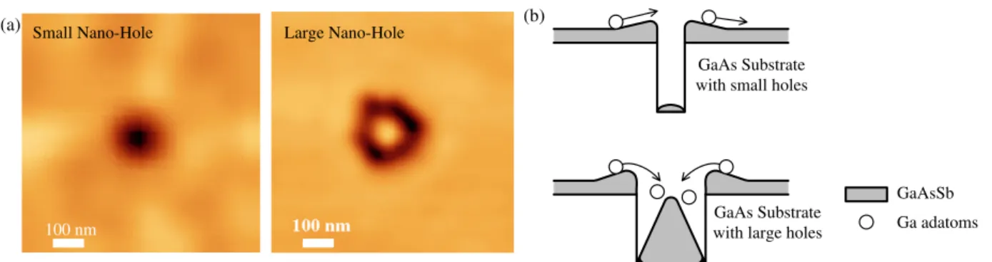
Small Nano-Hole Large Nano-Hole
100 nm
(a) (b)
GaAs Substrate with small holes
GaAsSb Ga adatoms GaAs Substrate
with large holes
Figure 2.(a) The AFM images of the samples with initial oxide height/diameter 4/150 and 7/180 nm after 15 nm GaSb buffer layer growth and (b) a schematic diagram describing the growth dynamics of the GaAsSb buffer layer.
0 0 0.5 0 0.5 1 2 3 4 5 0 1 2 3 4 5 Nano-oxides Site-controlled QDs (µm) (a) (b) GaAs/GaAsSb Buffer InAs
Figure 3.(a) The AFM image of the sample with a structure of 1.3 ML InAs/5 nm GaAs/15 nm GaAsSb and (b) a schematic diagram describing the growth evolution of the site-controlled QDs.
incorporation of Sb has facilitated adatom migration on the pre-patterned substrates [12]. As shown in the figure, an atomically-flat RMS roughness value of 0.3 nm is obtained for the samples with GaAsSb buffers thicker than 5 nm.
With the smooth surfaces obtained after GaAsSb buffer layer growth, the next issue would be the influence of the nano-hole sizes. The AFM images of the samples with initial oxide height/diameter 4/150 and 7/180 nm after 15 nm GaAsSb buffer layer growth are shown in figure 2(a). As shown in the figure, nano-holes are observed for the sample with smaller initial oxide sizes, while pillar structures are observed at the hole centers of the sample with larger initial oxide sizes. The results suggest that although enhanced adatom migration is obtained through the incorporation of Sb atoms into the buffer layers, some of the adatoms would still be trapped in the larger holes such that pillar structures would be observed. To explain the growth dynamics of the buffer layers on the substrates with smaller and larger nano-holes, a schematic diagram is shown in figure2(b). As shown in the figure, when the initial oxide size is smaller, smaller hole depth/diameter are obtained. For such samples, although the Ga adatoms tend to migrate to the holes, the holes are too shallow to trap the adatoms. In this case, most of Ga adatoms would undergo nucleation at the un-patterned regions without fully covering the small holes. However, for the sample with larger initial oxide sizes, a larger portion of the Ga adatoms would be trapped in the larger holes and undergo nucleation. In this case, pillar structures at the hole centers would be observed after buffer layer growth, which is disadvantageous for the site-controlled QD growth. The results
suggest that besides a smooth surface, the size of the nano-oxides is another key issue for the growth of site-controlled QDs.
Although GaAsSb buffer layer growth on patterned GaAs substrates could provide atomically-flat surfaces, it has been reported elsewhere that a higher InAs dot density would be observed on Sb-irradiated GaAs surfaces [12]. This phenomenon is disadvantageous for the fabrication of low-density site-controlled QDs. Therefore, the other thin GaAs layer grown after GaAsSb buffer layer growth would be necessary to replace the GaAsSb surfaces with GaAs surfaces. The AFM image of a sample with the structure of 1.3 ML InAs/5 nm GaAs/15 nm GaAsSb grown on a GaAs substrate with initial oxide height/diameter 4/150 nm and 1 µm separation is shown in figure 3(a). The AFM image of the sample after AFM nano-oxidation is also shown in the figure for comparison. As shown in the figure, site-controlled self-assembled QDs are observed with a 1µm hole separation. To explain the growth dynamics of the InAs QDs, a schematic diagram is shown in figure3(b). Since the InAs coverage is still below the critical thickness for QD formation, the appearance of QDs on the hole locations suggests that the In adatoms would migrate to the holes. In this case, the effective coverage near the holes would exceed a critical thickness such that QD selective growth would occur around the hole location. With increasing In adatom deposition, the small QDs would coalesce such that a single QD would be observed at the hole location. Also observed in the AFM image is the smooth surface of the sample after 5 nm GaAs deposition. The results suggest
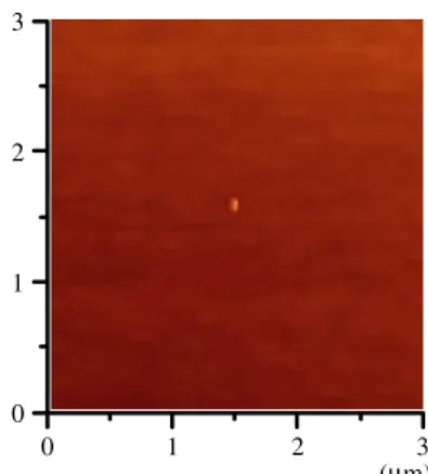
Nanotechnology 21 (2010) 295304 S-Y Lin et al 0 1 2 3 0 1 2 3 (µm)
Figure 4.A 3× 3 µm2AFM image of a single QD grown on a GaAs
substrate with 2µm hole separations. The wafer structure is of 1.3 ML InAs/5 nm GaAs/15 nm GaAsSb.
that after GaAsSb buffer layer growth, atomically-flat surfaces could be maintained even with additional GaAs layer growth.
The other important issue remaining for the site-controlled QD growth is how large the hole separation could be such that no QD formation would be observed on the un-patterned regions. A 3× 3 µm2 AFM image of a single QD grown
on a GaAs substrate with 2 µm hole separation is shown in figure4. The wafer structure of the sample is the same as the one discussed in the last paragraph. The single QD observed in the 3× 3 µm2AFM image suggest that under current growth
conditions, QD selective growth could be achieved with 1– 2µm separation. The results would be an effectively low dot density 1×107cm−2. Even larger separations may be achieved by changing the growth conditions to enhance the migration lengths of the In adatoms.
4. Conclusions
In conclusion, atomically-flat surfaces are obtained after thin GaAsSb buffer layer growth on GaAs substrates with regular-distributed nano-holes formed after oxide desorption in the
MBE chamber of the local AFM anode oxidation. By using substrates with nano-holes after GaAs/GaAsSb buffer layer growth, site-controlled self-assembled InAs QDs are observed with the deposition of a below-critical-thickness InAs coverage of 1.3 ML. An ultra low dot density 1× 107cm−2is observed for the sample. The results of site-controlled self-assembled InAs QDs on GaAs substrates by using traditional MBE growth procedures have facilitated the fabrication of site-controlled QDs, which is advantageous for the development of large-area high-performance single QD devices.
Acknowledgments
This work was supported in part by the National Science Council, Taiwan under grant numbers NSC 98-2221-E-001-001 and NSC 99-2911-I-98-2221-E-001-001-010.
References
[1] Leon R and Fafard S 1998 Phys. Rev. B58R1726
[2] Gong Q, N¨otzel R, Hamhuis G J, Eijkemans T J and Wolter J H 2002 Appl. Phys. Lett.811887
[3] Hsieh T O, Chiu P C, Chyi J I, Chang H S, Chen W Y, Hsu T M and Chang W H 2006 Appl. Phys. Lett.89053110
[4] Lin S Y, Lin W H, Tseng C C, Chao K P and Mai S C 2009
Appl. Phys. Lett.95123504
[5] Hsieh T P, Chyi J I, Chang H S, Chen W Y, Hsu T M and Chang W H 2007 Appl. Phys. Lett.90073105
[6] Kiravittaya S, Benyoucef M, Zapf-Gottwick R, Rastelli A and Schmidt O G 2006 Appl. Phys. Lett.89233102
[7] Kohmoto S, Nakamura H, Ishikawa T and Asakawa K 1999
Appl. Phys. Lett.753488
[8] Yang T, Kohmoto S, Nakamura H and Asakawa K 2003
J. Appl. Phys.931190
[9] Kim J S, Kawabe M and Koguchi N 2006 Appl. Phys. Lett.
88072107
[10] Mart´ın-S´anchez J, Alonso-Gonz´alez P, Herranz J, Gonz´alez Y and Gonz´alez L 2009 Nanotechnology
20125302
[11] Bimberg D, Grundmann M and Ledentsov N 1999
Quantum-Dot Heterostructure (New York: Wiley)
[12] Guimard D, Nishioka M, Tsukamoto M and Arakawa Y 2006
Appl. Phys. Lett.89183124