Single-Mode, High-Speed, and High-Power
Vertical-Cavity Surface-Emitting Lasers
at 850 nm for Short to Medium Reach
(2 km) Optical Interconnects
Jin-Wei Shi, Senior Member, IEEE, Zhi-Rui Wei, Kai-Lun Chi, Jia-Wei Jiang, Jhih-Min Wun, I-Cheng Lu,
Jason (Jyehong) Chen, and Ying-Jay Yang
Abstract—The vertical-cavity surface-emitting lasers (VCSELs)
with high single-mode (narrow linewidth) output power are essen-tial to minimize chromatic dispersion and to further improve the bit-rate distance product in a multimode fiber, which has a signif-icant propagation loss (∼3.5 dB/km) at 850 nm wavelength. Here, we demonstrate the detailed design considerations and fabrica-tion of a single-mode, high-power, and high-speed VCSELs at the 850 nm wavelength with oxide-relief and Zn-diffusion apertures for the application of short (0.3 km) to medium reach (2 km) optical interconnects. By optimizing the relative geometric sizes between two such apertures in our demonstrated 850-nm VCSELs, we can not only attain high single-mode output power (∼6.5 mW), but also with a reasonable threshold current (< 2.0 mA). Furthermore, the spatial hole burning effect induced low-frequency roll off can also be minimized in our optimized structure to obtain a maximum data rate up to 26 Gbit/s. The record-high bit rate-distance products for OM4 MMF transmission under ON–OFF keying (14 Gbit/s× 2.0 km) modulation formats have been successfully demonstrated by the use of our VCSEL.
Index Terms—Semiconductor lasers, vertical-cavity
surface-emitting lasers (VCSELs).
I. INTRODUCTION
T
HE relentless growth of the global internet traffic is now determined by a new wave of traffic growth fueled by lat-est applications targeted at the mobile internet systems, cloud computing, and social networks. Both the number and size of warehouse-scale data centers have been rapidly increased. Note that a warehouse-scale data center could consist of either oneManuscript received June 27, 2013; revised August 27, 2013; accepted September 5, 2013. Date of publication September 9, 2013; date of current version November 27, 2013. This work was sponsored in part by the Ministry of Economic Affairs of Taiwan under Grant 98-EC-17-A-07-S1–001 and in part by the National Science Council of Taiwan under Grant 101–2221-E-009–011-MY3.
J.-W. Shi, Z.-R. Wei, K.-L. Chi, J.-W. Jiang, and J.-M. Wun are with the Department of Electrical Engineering, National Central University, Zhongli 320, Taiwan (e-mail: [email protected]; [email protected]; [email protected]; [email protected]; [email protected]).
I.-C. Lu and J. J. Chen are with the Department of Photonics, National Chiao-Tung University, Hsinchu 300, Taiwan (e-mail: [email protected]; [email protected]).
Y.-J. Yang is with the Department of Electrical Engineering, National Taiwan University, Taipei 106, Taiwan (e-mail: [email protected]).
Color versions of one or more of the figures in this paper are available online at http://ieeexplore.ieee.org.
Digital Object Identifier 10.1109/JLT.2013.2281235
building or multiple buildings so the reach requirements for the data center ranges from 10 m to 2 km [1]–[3]. The active optical cable (AOC), which is mainly composed of vertical-cavity surface-emitting lasers (VCSELs) and multi-mode fibers (MMF), are considered the most promising candidates for high-capacity applications in very short-reach (VSR: < 300 m) fiber communication because of the combination of low-power con-sumption with wide-bandwidth performance [1]–[3]. Currently, the maximum transmission distance of a VCSEL-based AOC at 10-Gbit/sec operation is around 300 m, and is mainly limited by the effective modal bandwidth (EMB) of the standard OM4 MMF (4700 MHz·km) [4].
Various proposals have been recommended to extend the reach to over 2 km. The matured 1300 nm edge-emitting dis-tributed feed-back (DFB) lasers, Si photonic techniques, and single-mode fiber (SMF) as one quick solution [1], [5], [6], [7]. Although the MMF has a higher cabling cost than that of SMF when the transmission distance is over 1 km, nonetheless, the drawbacks of high-power consumption of edge-emitting lasers, small alignment tolerance, and high package cost for SMF-based AOCs still drive research efforts to extend the reach of the low-power consumption VCSEL-based MMF AOC up to several km [2]. One of the most straightforward ways to fur-ther narrow down the laser linewidth, minimize the chromatic dispersion in MMF, increase the bit-rate transmission distance product, and reduce the power consumption is to ultimately re-duce the diameter of the oxide current-confined aperture of the VCSEL [8], [9]. However, the minimum feature size of the ox-ide diameter is usually limited to 2 μm. A further downscale in size would lead to a large device resistance and would also make it difficult to be realized due to the uniformity issue of the oxi-dation process across the whole chip or wafer. 20(25) Gbit/s error-free transmissions through OM4 MMF as long as 1.1 (1) km obtained using this miniaturized VCSEL has been re-ported [9]–[11]. Nevertheless, the limited (quasi) single-mode output power (<2 mW) of these miniaturized VCSELs [8]–[11] may limit the further increase in maximum transmission distance up to > 2 km due to a significant transmission loss (3.5 dB/km) of 850 nm wavelength in the OM4 fiber [4]. We can thus un-derstand that it is very important to obtain a VCSEL with high single-mode output power, high modulation speed, low-power consumption, and extremely small linewidth performance. Such a device would let the VCSEL-based MMF AOC compete with
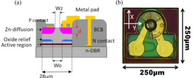
Fig. 1. (a) A conceptual cross-sectional view and (b) top-view of the demon-strated device.
the 1.3 μm DFB-based SMF AOC for the medium reach (2 km) optical interconnect market. Several methods, such as surface relief structures [12], [13], triangular holey structures [14], and antiresonant reflecting optical waveguide structures [15], have been utilized to fabricate VCSELs with a relatively large active diameter, a (near) single-mode, and high-output optical power performance. However, not all the reported single-mode and power VCSEL structures may be suitable for the high-speed applications. In this paper, we demonstrate the detail design considerations and fabrication of a novel single-mode output power and high-speed VCSEL operating at the 850 nm wavelength with oxide-relief and Zn-diffusion [16] structures to overcome the aforementioned limitations of VCSELs for the bit-rate transmission distance product. By optimizing the rela-tive sizes between the oxide-relief and Zn-diffusion apertures, a reasonable threshold current (< 2.0 mA), excellent side-mode suppression ratio (SMSR> 30 dB; from threshold to satura-tion), narrow spectral width (<0.08 nm; under large signal modulation), and high maximum single-mode power (6.7 mW) can be achieved. Furthermore, the spatial hole burning effect induced low-frequency roll off, which is usually observed in the electrical-to-optical (E–O) response of high-power (quasi-) single-mode 850 nm VCSELs [17]–[20], can be minimized. By use of our demonstrated device, record-high bit rate-distance products under ON–OFF keying (OOK) (14 Gbit/sec× 2.0 km) for OM4 MMF error-free transmission have been successfully demonstrated.
II. DEVICESTRUCTURE ANDFABRICATION
Fig. 1(a) and (b) shows the conceptual cross sectional and top views of the demonstrated device, respectively. As shown in Fig. 1(a), there are three key parameters; WZ, WO, and d,
which determine the mode characteristics of the device. Here, WZ and WOrepresent the diameter of the Zn-diffusion aperture
and oxide-confined aperture, respectively; d is the Zn-diffusion depth. In order to attain stable single-mode performance under the whole range of bias currents and eliminate the spatial hole burning effect, the relative sizes of these three parameters must be carefully optimized, which will be discussed later. Table I includes the detail geometric structure of the five devices (A to E) studied in this paper, which were fabricated from the same 850 VCSEL epitaxial wafer but diced with different five pieces for each device structure during processing. Our epi-layer
Fig. 2. (a) SEM image of the DBR structure with the oxide current-confined layer before and after performing the oxide-relief process. (b) SEM image of DBR layers after performing the Zn-diffusion process.
structure, purchased from IQE (IEGENS-7–20), is composed of three GaAs (60 ˚A)/Al0.3Ga0.7As (80 ˚A)
multiple-quantum-wells (MQWs) with a central wavelength at 835 nm and 1.5λ (wavelength) cavity length sandwiched between a 30-pair n-type and a 20-pair p-type Al0.9Ga0.1As/ Al0.12Ga0.88As
distributed-Bragg-reflector (DBR) layers with an Al0.98Ga0.02As layer
(30 nm thickness) just above the MQWs for oxidation. The whole structure is grown on an n+ GaAs substrate. For details
of the device fabrication processes, please refer to our previous work [16], [17]. As shown in Fig. 1(a), all five devices have the same single mesa structure with a 28 μm active diameter. The oxide-relief process was used to selectively remove the AlxO1−x
current confined layer. Due to the fact that the refractive index of air is much smaller than that of the AlxO1−xlayer (1 versus
1.6 [21]), there is a further reduction in the parasitic capacitance of the oxide-relief device [16]. Fig. 2(a) shows the scanning electron microscopic (SEM) picture of our oxide aperture be-fore and after the oxide relief process. As can be seen, after the relief process the oxide current confined layers and the edge of DBR layers with high Al concentration, which were oxidized during the oxidation process, were etched away.
Compared with the typical oxide-confined VCSEL, the addi-tional Zn-diffusion aperture in our structure allows us to real-ize mode control. The lasing phenomenon is suppressed in the Zn-diffused DBR region. The threshold gain becomes higher
Fig. 3. Characteristics of the optical output power (L) and voltage (V ) versus biasing current (I ) of devices A (Wz/Wo/d = 5/5.5/1 μm) and B (Wz/Wo/d =
5/5.5/1 μm).
due to the increase in free-carrier absorption loss and reduc-tion in reflectivity after the diffusion (DBR disordering) pro-cess [16], [17]. Fig. 2(b) shows an SEM cross-sectional view of the DBR region. Here, we adopt high quality Si3N4 as the
diffusion mask. The diffusion time and temperature is 30 min and 650◦C, respectively. As can be seen, there is a significant difference in the DBR layers with and without a Si3N4covering.
In the region without the Si3N4 covering, the phenomenon of
disordering is very clear and the depth in the lateral and per-pendicular directions is around 1.1 and 2.2 μm, respectively. As shown in Fig. 1(a), the fabricated device has a 28 μm diameter single active mesa on the n-type DBR layers. The top-view [see Fig. 1(b)] of the fabricated device shows the integrated slot line pads for on-wafer high-speed measurement.
III. MEASUREMENTRESULTS FOROXIDE-RELIEF AND
NONRELIEFDEVICES
As discussed previously, the oxide-relief process can reduce the parasitic capacitance of VCSELs and further enhance their speed performance. However, the relief process results in a more significant index contrast in the current-confined regime. This might induce more optical transverse modes in the cavity and make the single-mode performance become more difficult. In order to investigate this effect, two kinds of device structure with (A) and without (B) oxide-relief processes were fabricated. These two devices have the same WZ, WO, and d of 5, 5.5, and
1.0 μm, respectively. Fig. 3 shows the measured power (voltage) versus current (L – I and V – I) curves of devices A (A1 and A2) and B (B1 and B2). The devices A1 (B1) and A2 (B2) represent a VCSEL with the same structure as device A (B) but are different devices on the same chip. In fact, the L – I and V – I performances are measured for each device structure (A and B). What we show here is the typical device L – I performance for structures A and B. The values of their differential resistance measured under a moderate bias current (6 mA) are also specified in this figure. As can be seen, the relief structure (device A) usually has slightly better L – I and V – I performances than the nonrelief structure (device B). Such result might be attributable to the oxide-relief process which can partially eliminate the defect states which exist at the interface between the current-confined oxide layers and semiconductor epitaxial layers. Slight improvements in the
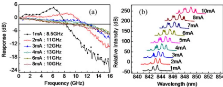
Fig. 4. Measured E – O frequency responses (a) and output optical spectra (b) of device A (Wz/Wo/d = 5/5.5/1 μm) under different bias currents.
Fig. 5. Measured E – O frequency responses (a) and output optical spectra (b) of device B (Wz/Wo/d = 5/5.5/1 μm) under different bias currents.
V – I performance, current injection efficiency into the active
layers, differential quantum efficiency, and output optical power can thus be observed in device A with the oxide-relief structure. Figs. 4 and 5 show the measured E–O frequency responses and optical spectra for devices A and B, respectively. The high-speed E–O performance of the fabricated devices was measured by a lightwave component analyzer, which was composed of a network analyzer (Anritsu 37397 C) and a calibrated 25GHz photoreceiver module (New focus 1481-S). We can clearly see that the optical mode spectra under different bias currents are very similar for the both devices, and due to the implementation of the Zn-diffusion process for optical mode control, both the devices exhibit quasi-single-mode behavior under the low bias current (< 3 mA) regime. Here, quasi-single-mode means that there are only two significant optical modes on the spectrum but the value of their SMSR is not as high as that of a single-mode VCSEL (SMSR > 30 dB). Compared with that of a typical multimode 850 nm VCSEL, this performance would benefit the transmission performance [9]–[11], [16] due to the narrower spectral width.
In addition, we can clearly see that device A has a slightly larger degree of red-shift in the measured spectra under a high bias current (10 mA). This phenomenon might be attributable to the different thermal expansion coefficient for the air gap and AlOx current confined region in devices A and B. After
per-forming the oxide-relief process, the DBR region can be treated as a cantilever structure, which should be more sensitive to the thermal expansion phenomenon than the nonrelief structure. A slightly larger degree of red-shift can thus be measured for de-vice A. In addition, in our case, such a phenomenon should not imply that the junction temperature (thermal impedance) in device A is higher than that of B. This is because that the
Fig. 6. Measured optical spectra (a) and L – I curve (b) of the reference device with a large difference in the sizes of WZ/WO/d (5.5/17/2 μm).
high-power performance of device A is even superior to that of B, as illustrated in Fig. 3.
According to the optical spectra measurement results, we can thus conclude that our oxide-relief process does not have a serious influence on the behavior of the optical modes, which can be attributed to the position of the oxide layer at the standing wave null in the DBR layers [20].
Furthermore, compared with device B, device A has a larger maximum 3-dB E–O bandwidth (12 versus 11 GHz) and a larger E–O bandwidth under (9 versus 8 GHz) and the same bias cur-rent, as low as 1 mA. This bandwidth improvement effect can be attributed to the reduction of the parasitic capacitance [16]. These dynamic and static measurement results clearly indicate that our oxide-relief process will not degrade the dc character-istics, which include L – I, V – I, and the output optical spectra of VCSELs and can significantly further improve the speed per-formance of the device.
IV. MEASUREMENTRESULTS OF THESINGLE-MODEDEVICE
In order to further extend the maximum transmission dis-tance in the OM4 fiber, a further optimization in the geometric sizes (Wz, Wo, and d) of device A to let it have single-mode
performance is highly desired. The key to achieve single-mode performance is to suppress the optical transverse modes inside the gain region (current-confined region) of the VCSEL cavity by the use of Zn-diffusion aperture, which can not only re-duce the reflectivity of DBR layers but also increase the free carrier absorption loss in the Zn-diffused area. Based on these points, we can expect that in order to have single-mode perfor-mance, we must let WO > WZ, which results in the significant
Zn-diffusion induced loss in the current-confined regime. In ad-dition, the size of WZ is also a criterion for the single-mode
performance. According to our previous work [17], the size of optical confined aperture (WZ) in our adopted epi-layer
struc-ture (IEGENS-7–20) must be smaller than 6.5 μm to ensure single-mode operation at 850 nm.
Fig. 6(a) shows the measured optical spectra under different bias currents of VCSEL with geometric size of WO = 17 μm,
WZ = 5.5 μm, and d = 2 μm. The oxide-relief process has also
been performed on this device. Fig. 6(b) shows the correspond-ing L – I curve for this VCSEL. As can be seen, a scorrespond-ingle-mode performance with SMSR far over 30 dB can be achieved un-der the full range of bias current. We can thus unun-derstand that the criterion of WO > WZ for single-mode performance would
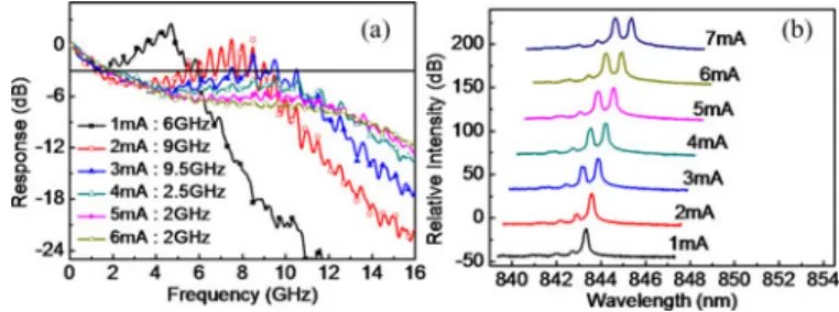
Fig. 7. Measured E–O frequency responses (a) and output optical spectra (b) of device C (Wz/Wo/d = 5/6.5/1 μm) under different bias currents.
Fig. 8. Measured L – I/V – I curves (a) and output optical spectra (b) of the single-mode device D (Wz/Wo/d = 6/8.5/2 μm) under different bias currents. result in serious intracavity loss (αi) and strongly suppress the
higher optical transverse modes which have an intensity peak in the peripheral region of the emission aperture (region with Zn-diffusion). However, such a large αi would induce a large
threshold current as large as 17 mA and a limited maximum output power, which limits its high-speed application for the optical interconnect.
Furthermore, the (quasi-) single-mode 850 nm VCSEL usu-ally suffers from the problem of low-frequency roll off in the E–O frequency response [17]–[20], which would degrade the eye-pattern quality during data transmission [17], [18]. Fig. 7(a) and (b) shows the measured E–O frequency responses and op-tical spectra under different bias currents for device C. The WZ, WO, and d of this device are 5, 6.5, and 1 μm, respectively,
and the oxide-relief process has also been performed. The ex-hibited L – I curves are similar to those for device A, as shown in Fig. 3. We can clearly see that when the bias current is less than 2 mA, the device exhibits single-mode behavior, accompa-nied by a serious low-frequency roll off in the measured E–O response, as expected. Under a 6 mA bias current, the 3 dB bandwidth degrades to only 2 GHz. According to the reported theoretical work [19], in order to minimize such phenomenon, a larger size of optical aperture (WZ) than that of current-confined
aperture (WO) is preferred. However, this condition is in
con-flict with our criterion of single-mode performance as discussed. Here, we adopt a different approach, which is to let the sizes of both the optical cavity (WZ) and current-confined aperture be
as large as possible and follow the criterion of single-mode per-formance (WZ < WO). We can expect the spatial hole burning
effect to be minimized due to the enlargement of cavity sizes and the reduction in carrier/photon density.
Figs. 8 and 9 show the measured L – I/V – I characteristics and optical spectra under different bias currents of devices D and E, respectively. Their geometric sizes (WO, WZ, and d)
Fig. 9. Measured L – I/V – I curves (a) and output optical spectra (b) of the single-mode device E (Wz/Wo/d = 5.5/8/2 μm) under different bias currents.
Fig. 10. Measured E–O frequency responses of devices D (Wz/Wo/d =
6/8.5/2 μm) (a) and E (Wz/Wo/d = 5.5/8/2 μm) (b) under different bias
currents
are specified in the two figure captions. The values of their differential resistance measured under a moderate bias current (6 mA) are also specified on these two figures. Different L – I and V – I curves represent the measurement results for different devices (D or E) fabricated on the same chips. The variation in device performance is mainly due to the processing issues or the nonuniformity in the VCSEL epi-wafer. Nevertheless, the yield for single-mode performance (SMSR > 30 dB) in the whole chip is very high (> 90%). As can be seen, these devices can sustain single-mode performance with a∼30 dB SMSR under the full range of bias current and have a reasonable threshold current at around 1.5 to 2.5 mA. The spectral width is measured by Advantest Q8384 optical spectrum analyzer with a smallest resolution of 0.01 nm. The measurement results for both of our proposed single mode VSCELs (D and E) is the same and as narrow as 0.08 nm (18.2 GHz spectral width), which is insensitive to the variation in bias currents. A sub-mA threshold current (∼0.5 mA) with excellent single-mode high-power performance (∼7 mW) has been demonstrated in our previous work [17] by further downscaling the size of WO and
WZ to < 6 and∼4 μm, respectively. However, such minimized
size of optical cavity would suffer from serious low-frequency roll off in the E–O response (when the bias current is >2 mA) due to its high photon density-induced spatial hole burning effect [17]–[19]. Fig. 10(a) and (b) shows the measured typical E–O frequency responses of devices D and E, respectively. We can clearly see that compared with device C, the low-frequency roll off effect has been greatly minimized in both devices (D and E). In addition, there are clear ripples (ringing) in the measured E–O frequency responses of these two single-mode VCSELs (devices D and E).
Such a result is in conflict with the smooth E – O responses (ripple free) of multimode devices (A and B), shown in Figs. 4 and 5. The observed ringing can be attributed to the
opti-Fig. 11. Measured far-field patterns of device D (Wz/Wo/d = 6/8.5/2 μm)
in the x- (a) and y- (b) directions under different bias currents.
Fig. 12. Measured back-to-back eye-patterns of devices A (Wz/Wo/d =
5/5.5/1 μm) and B (Wz/Wo/d = 5/5.5/1 μm) under 15 Gbit/s operation and
different bias currents.
cal feedback effect, which should be more pronounced in the single-mode device than the multimode device, due to its much longer coherent length (time) [22]. In order to suppress the feedback effect, an optical isolator is usually integrated with the single-mode laser during the high-speed measurement and data transmission [23].
Compared with device E, the roll off phenomenon in device D is less significant due to the larger size of the oxide (Wo) and
Zn-diffusion (Wz) apertures. The large active volume of device
D for single-mode performance also implies a narrow far-field divergence angle. Fig. 11(a) and (b) shows the measured far field patterns for device D in the x- and y-directions, respectively. These two directions are specified on Fig. 1(b). We can clearly see that the measured full-width half maximum of the divergence angle is as narrow as 6◦under the full range of bias current.
This value is narrower than that of our reported (6 versus 8◦) single-mode VCSEL with a smaller diameter of optical aperture (WZ: 4.5 versus 6.0 μm) [17].
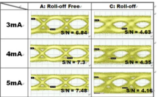
For the eye-pattern measurement, we used a 25 GHz pho-toreceiver module (New focus 1481-S) connected with a wide-band (100 kHz to 65 GHz) radio frequency amplifier (Centellax, UA0L65VM) to serve as our photoreceiver. Fig. 12 shows the measured back-to-back and error-free eye-patterns of devices A and B under different bias currents at the same data rate as 15 Gbit/s. We can clearly see that the measured eye-patterns of de-vice A have a shorter rise/fall time and a higher signal-to-noise (S/N) ratio than those of device B. The superior eye-pattern per-formance of device A compared to device B can be attributed to the better speed performance of device A as discussed in Figs. 4 and 5. The low-frequency roll off phenomenon also has a seri-ous influence on the measured eye-patterns. Fig. 13 shows the
Fig. 13. Measured back-to-back eye-patterns of devices A (Wz/Wo/d =
5/5.5/1 μm) and C (Wz/Wo/d = 5/6.5/1 μm) under 12.5 Gbit/s operation and
different bias currents.
Fig. 14. (a) Measured values of –log (BER) of device A (Wz/Wo/d =
5/5.5/1 μm) through 0.8 km OM4 fiber transmission at 15 Gbit/s and under dif-ferent bias currents. The inset shows the corresponding error-free eye-pattern. (b) Measured error-free eye-pattern of device C (Wz/Wo/d = 5/6.5/1 μm)
through 0.3 km OM4 fiber transmission at 15 Gbit/s operations and under 4 mA bias current.
measured back-to-back and error-free eye-patterns of device A (roll off free) and C (roll off) under different bias currents at the same data rate of 12.5 Gbit/s. We can clearly see that the mea-sured eye-patterns of device A have a much higher S/N ratio than that of device C. Furthermore, in contrast to device A, the S/N ratio of device C degrades with the increase of bias current. This result is mainly due to the observation that the low-frequency roll off phenomenon becomes more serious with the increase of bias current, as seen in Fig. 7. Based on this measurement result, we can thus conclude that the roll off phenomenon in the E – O response of VCSEL would seriously degrade its trans-mission performance.
Fig. 14(a) shows the measured –log [bit-error-rate (BER)] of device A under different bias currents obtained using an OM4 fiber with a maximum error-free transmission length (0.8 km) at 15 Gbit/s. Here, error free is defined as BER< 1× 10⁻¹². The inset shows the corresponding error-free eye-patterns. As can be seen, there is a BER floor (1× 10⁻¹²) in our measured BER curve, which originated from the satiability of our measure-ment system. During measuremeasure-ment, in order to get the values of BER as low as 1× 10⁻¹², a careful and stable optical align-ment over several minutes for error counting is necessary. Such alignment would not only determine the number of launched optical modes into the OM4 fiber but also the influence on the optical feedback effect. Any vibration of the instrument during error counting, such as the lens fiber, would lead to a serious in-crease in the BER value. It thus becomes a limitation in our BER
Fig. 15. (a) Measured values of –log (BER) of device D (Wz/Wo/d =
6/8.5/2 μm) through 2.0 km OM4 fiber transmission at 14 Gbit/s and under dif-ferent bias currents. The inset shows the corresponding error-free eye-pattern. (b) Measured back-to-back error-free eye-pattern of device D (Wz/Wo/d =
6/8.5/2 μm) with maximum data rate operation (26 Gbit/s).
values (floor). There are several possible ways to further improve the BER performance, such as more robust device packaging, selection of the optical mode for excitations [24], and integra-tion of the optical isolator with laser [23]. Fig. 14(b) shows the measured error-free eye-pattern of device C after the maximum length (0.3 km) of OM4 fiber transmission at the same data rate as 15 Gbit/s. We can clearly see that although device C has a narrower spectral width under low bias current than that of device A, it has a much poorer transmission performance (0.3 versus 0.8 km) due to the low-frequency roll off phenomenon. According to these measurement results, we can conclude that the high-power single-mode (narrow spectral width) output and roll off free performances are both important issues to further extend the bit-rate distance product of transmission. Fig. 15(a) shows the measured –log (BER) and the measured optical power at the receiver end versus bias current of device D after OM4 fiber transmission. The values of power shown on the figure in-clude the coupling loss between the VCSEL and OM4 fiber and 2 km fiber propagation loss (∼7 dB) at 850 nm wavelength. As can be seen, due to the excellent single-mode and high-power performance of our device, it can offer a large (∼10 dB) power budget at the receiver-end, which usually has a sensitivity of around −10 dBm, to mitigate the power penalty induced by fiber transmission (loss and dispersion). The insets show the corresponding error-free eye-patterns under the operation con-ditions with the lowest bias current (power consumption) for 14 Gbit/s operations. Fig. 15(b) shows the back-to-back error-free transmission result of device D at maximum data rate of 26 Gbit/s. Thanks to the excellent single-mode and roll off free performances of device D, record-high bit-rate distance product (14 Gbit/s× 2.0 km) through standard OM4 fiber by using OOK modulation scheme at 850 nm wavelength has been successfully demonstrated. In order to further determine the theoretical max-imum bit-rate distance product of our system and exact values of EMB of fiber used in our transmission experiment, a differential mode delay measurement [25] is necessary. This will be left for the future work.
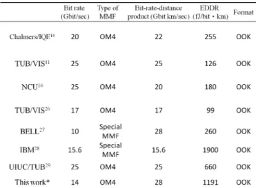
Table II shows the benchmark of bit-rate distance products and energy-to-data distance ratio (EDDR) [fJ/(bit.km)] [16], [26] by use of high-speed 850 nm VCSEL and OOK modula-tion format with error-free performance through MMF reported by different research groups [9]–[11], [16], [26]–[29]. For a detailed definition of EDDR, refer to [16] and [26]. We can
TABLE II
COMPARISON OFBIT-RATE-DISTANCEPRODUCT ANDPOWERCONSUMPTION OFMMF TRANSMISSIONBYUSING850NMVCSELS
clearly see that to further reduce the required driving current for error-free operation of our demonstrated single-mode VCSEL is an important next step to reduce the power consumption while maintaining such high bandwidth-distance product. This might be achieved by the integration of an additional optical isola-tor with our single-mode laser to suppress the optical feedback effect induced power penalty [23].
V. CONCLUSION
In conclusion, we demonstrate a novel VCSEL structure with high-speed and high single-mode power performance for medium-reach (2 km) data transmission through standard OM4 MMFs. By using the Zn-diffusion and oxide-relief techniques in our demonstrated VCSEL, we can manipulate the number of optical modes and enhance the device modulation speed, respectively. Furthermore, the demonstrated oxide-relief pro-cess can even improve the V – I and L – I performances as compared to those of nonrelief device without inducing optical higher order modes. By optimizing the relative sizes between Zn-diffusion and oxide-relief apertures, the 850 nm VCSEL with high single-mode output power and low-frequency roll off free performances under the full range of bias current has been demonstrated. The record-high error-free bit-rate distance prod-uct performance over a standard OM4 fiber by use of the OOK modulation format can be achieved by the use of our demon-strated device.
REFERENCES
[1] M. A. Taubenblatt, “Optical interconnects for high-performance comput-ing,” J. Lightw. Technol., vol. 30, no. 4, pp. 448–458, Feb. 2012. [2] D. Bimberg, “Green data and computer communication,” presented at
IEEE Photonic Soc. Meeting, Arlington, VA, USA, Oct. 2011, Paper TuN3.
[3] K. Kurata, “High-Speed optical transceiver and systems for optical inter-connects,” presented at Opt. Fiber Commun., San Diego, CA, USA, Mar. 2010, Paper OThS3.
[4] D. Molin, L.-A. de Montmorillon, and P. Sillard, “Low bending sensitivity of regular OM3/OM4 fibers in 10 GbE applications,” presented at Opt. Fiber Commun., San Diego, CA, USA, Mar. 2010, Paper JThA55.
[5] W. Kobayashi, T. Tadokoro, T. Fujisawa, N. Fujiwara, T. Yamanaka, and F. Kano, “40-Gbps direct modulation of 1.3-μm InGaAlAs DFB laser in compact To-CAN package,” presented at Opt. Fiber Commun., Los Angeles, CA, USA, Mar. 2011, Paper OWD2.
[6] Y. Lee, D. Kawamura, T. Takai, K. Kogo, K. Adachi, T. Sugawara, N. Chujo, Y. Matsuoka, S. Hamamura, K. Yamazaki, Y. Ishigami, T. Takemoto, F. Yuki, H. Yamashita, and S. Tsuji, “25-Gb/s 100-m MMF transmission using a prototype 1.3-μm-Range CMOS-Based transceiver for optical interconnections,” IEEE Photon. Technol. Lett., vol. 24, no. 6, pp. 467–469, Mar. 2012.
[7] A. Mekis, S. Abdalla, D. Foltz, S. Gloeckner, S. Hovey, S. Jackson, Y. Liang, M. Mack, G. Masini, M. Peterson, T. Pinguet, S. Sahni, M. Sharp, P. Sun, D. Tan, L. Verslegers, B. P. Welch, K. Yokoyama, S. Yu, and P. M. De Dobbelaere, “A CMOS photonics platform for High-Speed Op-tical Interconnects,” presented at IEEE Photonic Soc. Meeting, San Fran-cisco, CA, USA, Sep. 2012, Paper TuQ2.
[8] P. Moser, W. Hofmann, P. Wolf, J. A. Lott, G. Larisch, A. Payusov, N. N. Ledentsov, and D. Bimberg, “81 fJ/bit energy-to-data ratio of 850 nm vertical-cavity surface-emitting lasers for optical interconnects,” Appl.
Phys. Lett., vol. 98, no. 23, p. 231106, Jun. 2011.
[9] P. Moser, J. A. Lott, P. Wolf, G. Larisch, A. Payusov, N. N. Ledentsov, and D. Bimberg, “Energy-Efficient oxide-confined 850-nm VCSELs for long-distance multimode fiber optical interconnects,” IEEE J. Sel.
Topics Quantum Electron., vol. 19, no. 2, Article 7900406, Mar./Apr.
2013.
[10] R. Safaisini, K. Szczerba, E. Haglund, P. Westbergh, J. S. Gustavsson, A. Larsson, and P. A. Andrekson, “20 Gbit/sec error-free operation of 850 nm oxide-confined VCSELs beyond 1 km of multimode fibre,”
Elec-tron. Lett., vol. 48, no. 19, pp. 1225–1227, Sep. 2012.
[11] P. Moser, P. Wolf, G. Larisch, H. Li, J.A. Lott, and D. Bimberg, “Energy efficient 850 nm VCSELs for error-free 30 Gb/s operation across 500 m of multimode optical fiber with 85 fJ of dissipated energy per bit,” in
Proc. IEEE Opt. Interconnects Conf., Coronado, CA, USA, May 2013,
pp. 13–14.
[12] ˚A. Haglund, J. S. Gustavsson, P. Modh, and A. Larsson, “Dynamic mode stability analysis of surface relief VCSELs under strong RF modulation,”
IEEE Photon. Technol. Lett., vol. 17, no. 8, pp. 1602–1604, Aug. 2005.
[13] E. Haglund, A. Haglund, P. Westbergh, J. S. Gustavsson, B. Kogel, and A. Larsson, “25 Gbit/s transmission over 500 m multimode fibre using 850 nm VCSEL with integrated mode filter,” Electron. Lett., vol. 48, no. 9, pp. 517–519, Apr. 2012.
[14] A. Furukawa, S. Sasaki, M. Hoshi, A. Matsuzono, K. Moritoh, and T. Baba, “High-power single-mode vertical-cavity surface-emitting lasers with tri-angular holey structure,” Appl. Phys. Lett., vol. 85, pp. 5161–5163, Nov. 2004.
[15] D. Zhou and L. J. Mawst, “High-power single-mode antiresonant reflect-ing optical waveguide-type vertical-cavity surface-emittreflect-ing lasers,” IEEE
J. Quantum Electron., vol. 38, no. 12, pp. 1599–1606, Dec. 2002.
[16] J.-W. Shi, J.-C. Yan, J.-M. Wun, J. J. Chen, and Y.-J. Yang, “Oxide-Relief and Zn-Diffusion 850 nm vertical-cavity surface-emitting lasers with extremely low energy-to-data-rate ratios for 40 Gbit/sec operations,”
IEEE J. Sel. Topics Quantum Electron., vol. 19, Article 7900208, Mar./Apr.
2013.
[17] J.-W. Shi, C.-C. Chen, Y.-S. Wu, S.-H. Guol, and Y.-J. Yang, “High-Power and high-speed Zn-diffusion single fundamental-mode vertical-cavity surface-emitting lasers at 850 nm wavelength,” IEEE Photon.
Tech-nol. Lett., vol. 20, no. 13, pp. 1121–1123, Jul. 2008.
[18] J. S. Gustavsson, ˚A. Haglund, J. Bengtsson, P. Modh, and A. Larsson, “Dy-namic behavior of fundamental-mode stabilized VCSELs using shallow surface relief,” IEEE J. Quantum Electron., vol. 40, no. 6, pp. 607–619, Jun. 2004.
[19] Y. Liu, W.-C. Ng, B. Klein, and K. Hess, “Effects of the spatial nonunifor-mity of optical transverse modes on the modulation response of vertical-cavity surface-emitting lasers,” IEEE J. Quantum Electron., vol. 39, no. 1, pp. 99–108, Jan. 2003.
[20] P. Westbergh, R. Safaisini, E. Haglund, J. S. Gustavsson, A. Larsson, M. Geen, R. Lawrence, and A Joel, “High-Speed oxide confined 850-nm VCSELs operating error-free at 40 Gb/s up to 85◦C,” IEEE Photon.
Technol. Lett., vol. 25, no. 8, pp. 768–771, Apr. 2013.
[21] A. Fiore, V. Berger, E. Rosencher, P. Bravetti, and J. Nagle, “Phase matching using an isotropic nonlinear optical material,” Nature, vol. 391, pp. 463–466, Jan. 1998.
[22] P. Bala Subrahmanyam, Y. Zhou, L. Chrostowski, and C. J. Chang-Hasnain, “VCSEL tolerance to optical feedback,” Electron. Lett., vol. 41, no. 21, pp. 1178–1179, Oct. 2005.
Commun., vol. 25, pp. 226–229, Dec. 2004.
[26] P. Moser, J. A. Lott, P. Wolf, G. Larisch, A. Payusov, N. N. Ledentsov, W. Hofmann, and D. Bimberg, “99 fJ/(bit.km) energy to data-distance ratio at 17 Gb/s across 1 km of multimode optical fiber with 850-nm single-mode VCSELs,” IEEE Photon. Technol. Lett., vol. 24, no. 1, pp. 19–21, Jan. 2012.
[27] G. Giaretta, R. Michalzik, and A. J. Ritger, “Long distance (2.8 km), short wavelength (0.85 μm) data transmission at 10 Gb/sec over new generation high bandwidth multimode fiber,” in Proc. Conf. Lasers Electro-Opt. OSA
Tech. Dig., San Francisco, CA, USA, May 2000, pp. 683–684.
[28] P. Pepeljugoski, D. Kuchta, Y. Kwark, P. Pleunis, and G. Kuyt, “15.6-Gb/s transmission over 1 km of next generation multimode fiber,” IEEE
Photon. Technol. Lett., vol. 14, no. 5, pp. 717–719, May 2002.
[29] M. P. Tan, J. A. Lott, S. T. M. Fryslie, N. N. Ledentsov, D. Bimberg, and K. D. Choquette, “25 Gb/s Transmission over 1-km OM4 multimode fiber using a single mode photonic crystal VCSEL,” presented at Proc. Conf. Lasers Electro-Opt. OSA Tech. Dig., San Jose, CA, USA, Jun. 2013, Paper CTu3L.3.
Jin-Wei Shi was born in Kaohsiung, Taiwan on January 22, 1976. He received
the B.S. degree in Electrical Engineering from National Taiwan University, Taipei, Taiwan in 1998 and the Ph.D. in Graduate Institute of Electro-Optical Engineering from National Taiwan University, Taipei, Taiwan in 2002. He was a Visiting Scholar at the University of California, Santa Barbara (UCSB), CA, during 2000 and 2001. In 2002-2003, he served as a post-doc researcher at Electronic Research & Service Organization (ERSO) of Industrial Technol-ogy Research Institute (ITRI). In 2003, he joined the Department of Electrical Engineering, National Central University, Taoyuan, Taiwan, where he is now professor. From 2011/02 to 2012/02, he joins the ECE Dept. of UCSB again as a Visiting Scholar. His current research interests include ultra-high speed/power optoelectronic devices, such as photodetectors, electro-absorption modulator, sub-millimeter wave photonic transmitter, and semiconductor laser. He has au-thored or co-auau-thored more than 100 Journal papers, 190 conference papers and hold 20 patents. He was the invited speaker of 2002 IEEE LEOS, 2005 SPIE Optics East, 2007 Asia-Pacific Microwave Photonic conference (AP-MWP), 2008 Asia Optical Fiber Communication & Optoelectronic Exposition & Con-ference (AOE), 2011 Optical Fiber Communication (OFC), 2012 Plastic Optical Fiber (POF), and 2012 IEEE Photonic Conference (IPC). He served as the tech-nical program committee of OFC 2009-2011, 2012 SSDM, 2012 MWP, and 2013 Asia-Pacific CLEO. He was the recipient of year 2007 Excellence Young Researcher Award from Association of Chinese IEEE and 2010 Da-You Wu Memorial Award
Zhi-Rui Wei has got his Master degree in Department of Electrical Engineering
at National Central University, Taoyuan, Taiwan, at Aug., 2013. His current research interests include high-speed optoelectronic device measurement and high-speed VCSELs and LEDs for the application of optical interconnects.
Jia-Wei Jiang is now working on the Master degree in Department of
Electri-cal Engineering at National Central University, Taoyuan, Taiwan. His current research interests include high-speed optoelectronic device measurement and high-speed VCSELs and LEDs for the application of optical interconnects.
Jhih-Min Wun was born in Taoyuan, Taiwan on Oct. 03, 1988. He is now
working on the PhD degree in Department of Electrical Engineering at National Central University, Taoyuan, Taiwan. His current research interests include high-speed optoelectronic device measurement and high-speed photodiode with sub-THz bandwidth.
I-Cheng Lu is now working on the PhD degree in Institute of Electro-Optical
engineering and department of photonics, Taiwan. His current research interests include fiber communication and high-speed VCSELs and DFBs for the appli-cation of optical interconnects.
Jason (Jyehong) Chen received his BS and MS degree in Electrical Engineering
from National Taiwan University, Taiwan, in 1988 and 1990 respectively and the Ph.D. degree in Electrical Engineering and Computer Science from University of Maryland Baltimore County, Maryland, USA, in 1998.
He joined JDSU in 1998 as senior engineer and obtained 10 U.S. patents in 2 years. He joined the faculty of National Chiao-Tung University, Taiwan, 2003, where he is currently a professor in the Institute of Electro-Optical engineering and department of photonics. Prof. Chen published more than 100 papers on international journals and conferences. His research interests focus on hybrid access network, long reach passive optical network and optical interconnects.
Ying-Jay Yang was born in I-Lan, Taiwan, in 1952. He received the B.S.
degree in electrical engineering from National Taiwan University in 1974, the M.S. degree and the Ph.D. degree in electrical engineering from North Carolina State University, in 1982 and 1987 respectively. During his Ph.D. work he invented the first quantum well Transverse Junction Stripe (TJS) lasers and also the first CW operation strained-layer TJS lasers. From 1987 to 1989 he was an engineer at Hewlett Packard, working on the development of 1.3 um InGaAsP LEDs for FDDI. From 1989 to 1993 he joined Lockheed Palo Alto Research Laboratory as a research scientist. He worked on the vertical-cavity surface emitting lasers (SELs), invented the first single transverse mode SELs and the first optoelectronic integration circuits (OEICs) with a SEL and a FET. Since February 1993 he joined the Department of Electrical Engineer, National Taiwan University, where he is now a professor. His current research areas are semiconductor materials, and devices including lasers, modulators, quantum devices, and OEICs.