國
立
交
通
大
學
電子工程學系 電子研究所
博 士 論 文
低溫合成之奈米碳管與薄膜側向場發射子之
場發射特性研究
Study on the Field Emission Characteristics of
Low-Temperature-Synthesized Carbon Nanotubes and Thin Film Edge
Field Emitters
研 究 生:林高照
指導教授:鄭晃忠 教授
低溫合成之奈米碳管與薄膜側向場發射子之
場發射特性研究
Study on the Field Emission Characteristics of
Low-Temperature-Synthesized Carbon Nanotubes and Thin Film Edge
Field Emitters
研 究 生:林高照 Student:Kao-Chao Lin
指導教授:鄭晃忠 Advisor:Huang-Chung Cheng
國 立 交 通 大 學
電子工程學系 電子研究所
博 士 論 文
A DissertationSubmitted to Department of Electronics Engineering and Institute of Electronics
College of Electrical and Computer Engineering National Chiao Tung University
in partial Fulfillment of the Requirements for the Degree of
Doctor of Philosophy in
Electronics Engineering
July 2008
Hsinchu, Taiwan, Republic of China
低溫合成之奈米碳管與薄膜側向場發射子之
場發射特性研究
研究生:林高照 指導教授:鄭晃忠 博士
國立交通大學電子工程學系暨電子研究所博士班
摘要
在本論文中,我們主要研究標的為場發射材料與場發射元件的低溫製作方法 與其場發射特性研究。為了可以均勻且低成本的將奈米碳管應用於場發射顯示器 上,熱化學氣相沈積比起其他方法具有簡單且低成本的優勢,因此被認為是最有 潛力的碳管成長方法之一。藉由多層結構催化金屬的使用,我們可利用熱化學氣 相沈積在低溫下於玻璃基板上合成奈米碳管。多層結構催化金屬的組成包含支撐 層、中間層與催化金屬,其中支撐層可以有效幫助催化金屬均勻分散避免其聚合 成過大的粒子,而中間層除了幫助催化金屬保持均勻分散外還可以促進碳原子的 析出進而形成石墨層結構,由實驗結果可以發現,當中間層材料為鉻與鈦時,奈 米碳管的型態是最佳的,同時其表現出絕佳的場發射特性:當所施加的電場強度 為 6 V/µm 時,其場發射電流密度分別可達到 18.24 與 28.60 mA/cm2,遠超過應 用上所需的數值。除此之外,碳管的場發射特性與外觀也會受到製程條件的影 響,如反應氣體流量。藉由逐步改變與控制製程氣體的流量比例,我們得到一組 最佳的成長參數,當製程氣體乙烯、氫氣與氮氣分別為 125、10 與 1000 sccm 時, 奈米碳管具有最好的電性表現:。實驗結果也說明場發射特性與碳管的結晶性有相當程度的關係,隨碳管結晶性增加其場發射電流的穩定性也跟著增加。同時, 碳管成長的活化能圖說明多層結構催化金屬具有較低的成長活化能,因此相較於 其他催化金屬可以有效於低溫下催化碳管成長。 接下來,為有效改善電子束發散的現象,我們提出一基於低溫成長奈米碳管 的自聚焦場發射元件,此一元件結構不需要額外的聚焦閘極而是採用將電極設計 成一雙條狀電極且平行於場發射區域旁,不同於傳統元件結構具有被閘極包圍的 場發射區域,自聚焦閘極結構因為條狀電極只鄰近單一邊的碳管,因此會造成異 於傳統的非對稱的場發射區,結合此兩個非對稱場發射區域,場發射電子將於陽 極板上形成一重疊的顯示區塊。從實驗結果來看,此一新穎閘極結構可以有效控 制電子束軌跡且於陽極板上形成較小的發光區。模擬結果說明相較於傳統沒有聚 焦結構的元件,當採用自聚焦閘極結構時陽極板上的場發射區域可由 622 微米縮 小至 232 微米,同時實際螢光版上的發亮區域也顯示出相同的實驗結果,因此證 明自對焦閘極結構可簡單且有效地控制電子束於陽極板上的大小。 最後,我們提出兩種形成次微米間距的方法並將其應用於製作具有低超作電 壓的薄膜側向場發射子。元件可藉由薄膜沈積與濕式蝕刻完成,且電極間距可由 蝕刻時間來控制,次微米間距形成於射極與集極間,當其間距為 200 奈米時,元 件的啟始場發射電壓可以降低到 48 伏特。此外,為了進一步更可靠地製作此一 次微米間距,我們提出一類平面側向場發射元件結構,此元件的電極間距可以藉 由薄膜的厚度來調變,不同的膜厚將形成不同的間距大小。另外,經由一形成製 程改變場發射子的表面型態,形成較高的表面粗糙度,元件的場發射特性可明顯 的改善。當控制電極間距此一膜層的厚度為 200 奈米時,經過形成製程處理的元 件,其場發射啟始電壓值可降低到 9 伏特。
Study on the Field Emission Characteristics of
Low-Temperature-Synthesized Carbon
Nanotubes and Thin Film Edge Field Emitters
Student: Kao-Chao Lin Advisor: Dr. Huang-Chung Cheng
Department of Electronics Engineering & Institute of Electronics
College of Electrical Engineering and Computer Science
National Chiao Tung University
ABSTRACT
In this thesis, low-temperature synthesis processes of emitter materials and devices as well as their field emission characteristics were investigated. For their application in field emission displays, carbon nanotubes (CNTs) should be employed uniformly on glass substrates in order to reduce the manufacture cost. Thermal chemical vapor deposition (t-CVD) had the merits of simplicity and cost efficiency in fabrication and large scalability as compared with other techniques. Therefore, it seemed to be a potential method for synthesizing nanotubes on glass substrates. Multilayer catalysts utilized in thermal CVD systems showed a remarkable catalytic ability for growth of CNTs at low temperatures. The multilayer catalysts were composed of supporting layer, interlayer, and catalytic metal. A supporting layer had the functionality in uniformly distribution of catalytic nanoparticles, meanwhile preventing their agglomeration. Besides improving the uniformity of catalytic particles, interlayers were able to enhance the precipitation of carbon atoms, thus
resulting in the formation of graphite sheets. According to the results of experiment, while the interlayers were chromium (Cr) and titanium (Ti), carbon nanotubes showed the better morphologies and field emission performances: field emission current density of 18.24 and 28.60 mA/cm2 for Cr and Ti, respectively, at the electric field of 6 V/µm. Moreover, field emission characteristics of nanotubes can be improved by optimizing the synthesis conditions, i.e. reaction gas flow rates. According to the results of experiments, an optimal synthesis condition formed of reaction gases was 125, 10, and 1000 sccm for C2H4, H2, and N2, respectively. The morphology and field
emission performance also showed a significant relationship corresponding to the crystallinity of nanotubed analyzed by Raman Spectra. A high stability of emission current was correlative with a better crystallinity. The growth activation energy calculated based on the dependence of nanotube length versus temperature revealed the fact that CNTs synthesized with a multilayer catalyst displayed a lower value than single or binary catalysts.
Next, a CNT-based device with a self-focusing gate structure was proposed to obviate the issue of electron beam divergence. Without additional focusing electrodes, the self-focusing gate structure employed a pair of gate electrodes parallel with the vicinity of emitters, which resulted in an asymmetric emission area as compared with the conventional gate structure. Therefore, electrons emitted from the emitters gave rise to an overlapping region on the anode plate so that a reduction of spot size had been achieved. According to the simulation results and luminescent images, this self-focusing gate structure had a well controllability on the trajectory of electrons, and therefore showed a smaller luminescent spot size than the conventional one. Because of the overlapping of electron beams, the luminescent spot sizes could be remarkably reduced to 232 µm in x direction as compared with 622 µm for the conventional gate structure which had a serious issue of beam divergence. As a result,
the self-focusing gate structure manufactured with a simple process can produce well-focused electron beams for the application in FEDs.
Finally, two simple techniques of creating sub-micron gaps were proposed for thin film edge emitters in order to realize the feasibility in low-voltage operation and simplicity in fabrication. A lateral field emitter was manufactured by thin film deposition and wet etching processes. The spacing was determined by the lateral etching distance formed during etching stage. By controlling the duration of etching, the distances between emitters and collectors were well defined in submicron ranges. Device performance showed a low turn-on voltage of 48 V at an emission current of 100 nA as the emitter-collector spacing was 200 nm. In addition, for creation of submicron gaps in a more robust way, a novel quasi-planar thin film field emitter was proposed and fabricated utilizing the similar idea. The spacing between the emitter and collector could be well controlled via the thickness of Cr layers, which created submicron gap. A forming process caused an increased surface roughness of emitters and resulted in a higher field enhancement factor, which showed better field emission characteristics. The quasi-planar field emission diode with the first Cr layer of 200 showed a low turn-on voltage of 9 V at the current level of 100 nA.
誌 謝
首先要感謝在國立交通大學以來所有教導過我的老師,尤其是我的指導教授 鄭晃忠博士。鄭教授對研究的積極專注以及實事求是的態度,深深影響著學生。 謝謝他在學術研究和為人處世方面的指導與鼓勵,才能使我順利地完成博士學 位。也感謝在百忙之中抽空參加我論文口試的委員們,有了委員們專業的建議與 熱心的指導,才能使我的論文更加地完整。 其次,我要感謝在奈米電子與顯示技術實驗室(NEDT Lab.)所有曾經相遇 的夥伴們。感謝國基、全平與鼎國學長於實驗上的指導與建議;也感謝一起奮鬥 的瑞霖學弟,幫我分擔不少事情;感謝宗穎學弟、翰忠學弟、耀星學弟、俠威學 弟、育瑛學妹、建穎學弟,有你們的協助實驗研究才得以順利進行;同時,也要 感謝耀仁學弟、鈞凱學弟、佩琪學妹、君翰學弟、加聰學弟、英彰學弟、萬霖學 弟與筠珊學妹等同組成員給予的建言與協助。 也感謝國瑞學長、志良學長、春乾同學與學弟妹們包含:柏廷、大傳、逸哲、 柏宇、育如、可玉、瑛君、旭信、凱方、祐祈、政欽、仕偉、序恆、偉凱以及其 他人等等,有你們在實驗與生活上的鼓勵和協助,漫長的求學生涯才顯得多采多 姿。 另外,我還要感謝交通大學奈米中心(NFC)與國家奈米元件實驗室(NDL) 提供完善的實驗設備,尤其要感謝所有交大奈米中心的技術人員們,特別是徐秀 巒小姐、黃月美小姐、陳聯珠小姐、范秀蘭小姐、鄭淑娟小姐、倪月珍小姐、陳 明麗小姐、陳月婷小姐、彭兆光先生、胡進章先生以及林聖欽先生在技術上的協 助,並在實驗設備及維護上給予最大的支持與配合,使我的研究得以順利完成。 以及行政人員劉曉玲小姐與何惟梅小姐在行政事物上的協助。 最後,要特別感謝我的最愛的家人們,林春義先生與劉桃女士以及雅卿、雅 淑,自我出生以來這些年來對我全力的支持與照顧,讓我於求學歷程中心無旁 騖,專心於學術研究上,能有今日學業上的成果。謹以此論文獻給我最愛的家人 與朋友們。Contents
Abstract (in Chinese)...i
Abstract (in English)...iii
Acknowledgments (in Chinese)...v
Contents...vii
Table Lists...xi
Figure Captions...xii
Chapter 1 Introduction
1.1 Overview of Vacuum Microelectronics………..1
1.2 Theory of Field Emission………3
1.3 Application of Vacuum Microelectronics………6
1.4 Field Emission Displays………..7
1.4.1 Technologies of Field Emission Displays………9
1.4.1.1 Cathode Structures………10
1.4.1.1.1 Spindt-Type Field Emitters……….10
1.4.1.1.2 Silicon Tip Field Emitters………11
1.4.1.1.3 MIM……….11
1.4.1.1.4 BSD……….12
1.4.1.1.5 Ferroelectric Emitters………..13
1.4.1.1.6 Planar (Lateral) Field Emitters………13
SCE………..14
Thin Film Edge Emitters………..15
1.4.1.2.1 Diamond and DLC……….15
1.4.1.2.2 Carbon Nanotubes………..16
1.5 Motivation………..18
1.6 Thesis Organization………20
Chapter 2 Investigation of Carbon Nanotubes Synthesized
at Low Temperatures Using Multi-layered Catalytic Films
2.1 Introduction………22
2.2 Experimental Procedures………25
2.2.1 Sample Fabrication………..25
2.2.2 Material Analysis……….26
2.3 Morphologies and Field Emission Characteristics of CNTs………..26
2.3.1 Effect of Supporting Layer……….26
2.3.2 Effect of Interlayer………..28
2.4 Growth Mechanism………31
2.5 Summary………32
Chapter 3 Improvements of Morphologies and Field
Emission Characteristics for Carbon Nanotubes by
Modifying the Gas Flow Rate Ratios
3.1 Introduction………..34
3.2 Experimental Procedures………..36
3.2.1 Sample Fabrication………36
3.3 Morphologies and Field Emission Characteristics of CNTs……….38
3.3.1 Effect of H
2………..38
3.3.2 Effect of N
2……….39
3.3.3 Effect of C
2H
4……….40
3.3.4 Effect of Temperature and Activation Energy……….40
3.4 Growth Mechanism………42
3.5 Summary………43
Chapter 4 Fabrication and Characterization of Carbon
Nanotube Field Emission Devices with a Self-Focusing Gate
Structure
4.1 Introduction………44
4.2 Concept of Beam Overlapping………...46
4.3 Experimental Procedures………47
4.3.1 Simulation………47
z Effect of Gate Width……….47
z Effect of Gate Spacing………..48
4.3.2 Device Fabrication and Analysis……….49
4.3.3 Device Performance………51
4.4 Summary………52
Chapter 5 Fabrication and Emission Characteristics of
Chromium Thin Film Edge Emitters
5.1 Introduction………54
5.2 Planar Edge Field Emitter………..56
5.2.1 Sample Fabrication and Analysis………56
5.2.2 Field Emission Characteristics………57
5.3 Quasi-Planar Edge Field Emitters………..58
5.3.1 Sample Fabrication and Analysis………58
5.3.2 Field Emission Characteristics………59
5.4 Summary………60
Chapter 6 Summary and Conclusions
………62
Chapter 7 Future Prospects
………66
References
………...
68
Tables
...
87
Figures
...
94
Vita
...
154
Publication Lists
………..155
Table Lists
Chapter 1
Table 1.1 Comparison between vacuum microelectronics and solid-state electronics………87 Table 1.2 The history of vacuum microelectronics……….88 Table 1.3 The comparison of several flat panel displays………89
Chapter 2
Table 2.1 Field emission characteristics of CNTs synthesized with different catalysts………90 Table 2.2 Field emission characteristics of CNTs synthesized with multilayer catalysts
consisting of different interlayers………90 Table 2.3 Field emission characteristics of CNTs synthesized with multilayer catalysts
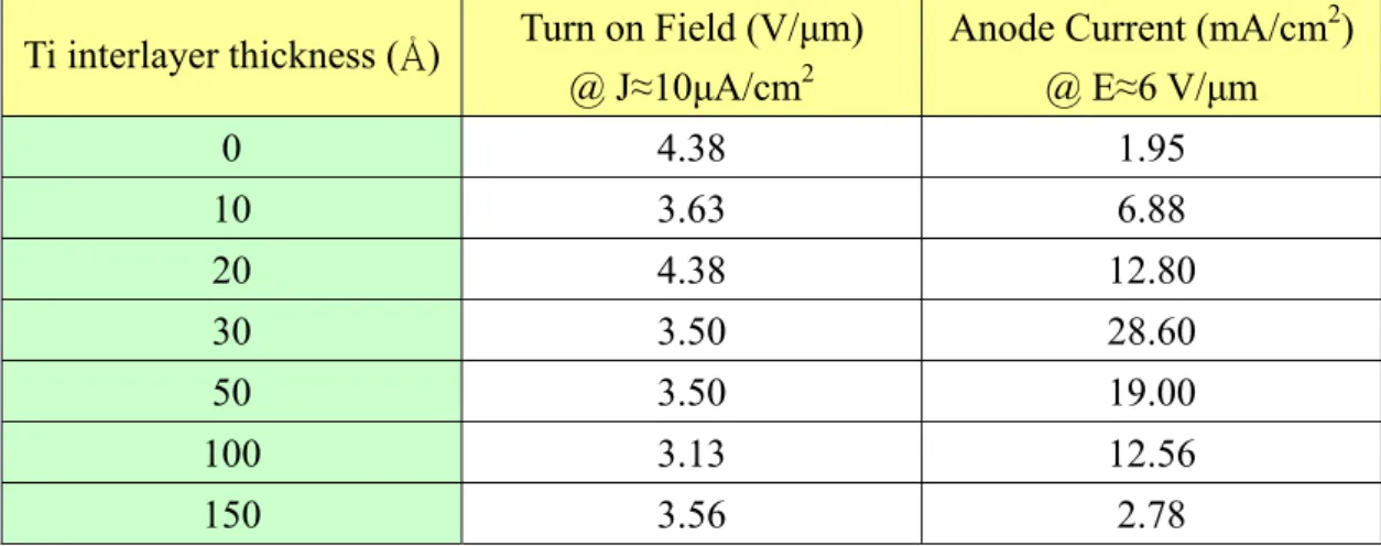
(Co/Cr/Al) consisting of different Cr interlayer thickness………..91 Table 2.4 Field emission characteristics of CNTs synthesized with multilayer catalysts
(Co/Ti/Al) consisting of different Ti interlayer thickness………...91 Table 2.5 Formation heat of metal carbides………92
Chapter 3
Table 3.1 Field emission characteristics of CNTs depending on the H2/N2 flow
ratios………93 Table 3.2 Field emission characteristics of CNTs depending on the N2 flow rates…93
Table 3.3 Field emission characteristics of CNTs depending on the C2H4 flow
Figure Captions
Chapter 1
Figure 1.1 Figure 1.1 The band diagram of the field-emission emitters in the vacuum environment (a) without applied electric field and (b) with applied electric field………94 Figure 1.2 A schematic illustration for the structures of (a) a cathode-ray tube and (b) a field-emission display……….95 Figure 1.3 The device structures of (a) diode-type and (b) triode-type in
field-emission displays. The main differences between the diode-type and the triode-type device structure are the gate electrode around the emitter which can extract electrons from the cathodes at relative low electric field………96 Figure 1.4 The micrographs taken by SEM for (a) Spindt field emitter arrays and (b)
device structure with higher resolution……….97 Figure 1.5 The schematic depiction of (a) the MIM device structure and (b) the
emission mechanism……….98 Figure 1.6 The schematic diagram of (a) the BSD device structure and (b) the
electron emission model………99 Figure 1.7 The schematic illustration of the ferroelectric emission mechanism. The
screening charges are developed to compensate the net charges and a fast reversal of the polarization results a large electric field that ejects the electrons from the negative charged surface………...100 Figure 1.8 The illustration of surface conduction emitters: (a) the device structure
and (b) the mechanism of surface conduction emission………101
Chapter 2
Figure 2.1 High-resolution SEM images of morphologies of catalysts after pretreatment: (a) 20Co, (b) 20Co/20Cr, (c) 20Co/100Al, and (d) 20Co/20Cr/100Al………102 Figure 2.2 High-resolution SEM images of surface morphologies of samples with
different Al supporting layer thickness after pretreatment: (a) 2 nm, (b) 5nm, (c) 10 nm, and (d) 20nm……….103 Figure 2.3 SEM images of surface morphologies of samples with different catalysts
after CNT synthesis process: (a) 20Co, (b) 20Co/20Cr, (c) 20Co/100Al, (d) 20Co/2oCr/20Al, (e) 20Co/20Cr/50Al, (f) 20Co/20Cr/100Al, and (g) 20Co/20Cr/200Al. (The scale bars in the insets represent 1μm)………...………104 Figure 2.4 Field emission characteristics of samples with different catalysts after
CNT synthesis process: (a) J-E curve and (b) FN plot………105 Figure 2.5 XPS analysis of the Al 2p peak for the sample with multilayer catalysts
(20Co/20Cr/100Al)……….106 Figure 2.6 SEM images of surface morphologies of samples with multilayer catalysts
consisting of different interlayer metals: (a) 2 nm W, (b) 2 nm Mo, (c) 2 nm Ta, (d) 2 nm Pt, (e) 2 nm Cr, (f) 2 nm Ti, (g) 2 nm Hf, (h) 2 nm Pd, and (i) 2 nm Cu. (The scale bars in the insets represent 2μm)………..………107 Figure 2.7 Field emission characteristics of samples with multilayer catalysts
consisting of different interlayer metals after CNT synthesis process: (a) J-E curve and (b) FN plot………108
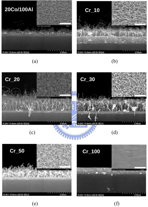
Figure 2.8 SEM images of surface morphologies of samples with multilayer catalysts consisting of different Cr interlayer thickness: (a) 0 nm, (b) 1 nm, (c) 2 nm, (d) 3 nm, (e) 5 nm, and (f) 10 nm. (The scale bars in the insets represent 2μm)………..…109 Figure 2.9 SEM images of surface morphologies of samples with multilayer catalysts
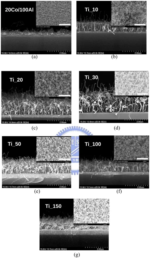
consisting of different Ti interlayer thickness: (a) 0 nm, (b) 1 nm, (c) 2 nm, (d) 3 nm, (e) 5 nm, (f) 10 nm, and (g) 15 nm. (The scale bars in the insets represent 2μm)……….……..110 Figure 2.10 Field emission characteristics of samples with multilayer catalysts
consisting of different Cr interlayer thickness after CNT synthesis process: (a) J-E curve and (b) FN plot………..111 Figure 2.11 Field emission characteristics of samples with multilayer catalysts
consisting of different Ti interlayer thickness after CNT synthesis process: (a) J-E curve and (b) FN plot……….112 Figure 2.12 (a) TEM images of CNTs synthesized with multilayer catalysts
(20Co/30Ti/100Al) consisting of 3 nm Ti interlayer, and (b) the EDS analysis of catalytic particle shown in (a)………..113 Figure 2.13 (a) TEM images of CNTs synthesized with multilayer catalysts
(20Co/30Cr/100Al) consisting of 3 nm Cr interlayer, and (b) the EDS analysis of catalytic particle shown in (a)………..114 Figure 2.14 XPS analysis of samples with multilayer catalysts consisting of (a) Ti
interlayer and (b) Cr interlayer………115 Figure 2.15 Surface energies of elements………...…116 Figure 2.16 Schematic diagrams of morphologies of catalytic nanoparticles formed
due to the difference of surface energies between catalytic thin film and interlayer thin films: (a) surface energy of interlayer thin film smaller than
that of Co, (b) surface energy of interlayer thin film close to that of Co, and (c) surface energy of interlayer thin film larger than that of Co…...117
Chapter 3
Figure 3.1 SEM images of surface morphologies of samples after CNT synthesis process conducted with different H2/N2 flow rate ratios: (a) 0/1000, (b)
10/990, (c) 20/980, and (d) 50/950. (The scale bars in the insets represent 2μm)……….……118 Figure 3.2 (a) J-E field emission characteristics of CNTs synthesized with different
H2 flow rates and (b) the corresponding FN plot………..119
Figure 3.3 (a) Raman analysis of samples after CNT synthesis process conducted with different H2/N2 flow rate ratios and (b) the plot of ID/IG intensity vs.
H2 flow rates………..120
Figure 3.4 SEM images of surface morphologies of samples after CNT synthesis process conducted with different N2 flow rates: (a) 0, (b) 250, (c) 500, (d)
750, (e) 1000, (f) 1250, (g) 1500, (h) 2000, and (i) 5000 sccm. (The scale bars in the insets represent 2μm)……….…121 Figure 3.5 Figure 3.5 (a) J-E field emission characteristics of CNTs synthesized with
different N2 flow rates and (b) the corresponding FN plot………122
Figure 3.6 (a) Raman analysis of samples after CNT synthesis process conducted with different N2 flow rates and (b) the plot of ID/IG intensity vs. N2 flow
rates………123 Figure 3.7 SEM images of surface morphologies of samples after CNT synthesis
process conducted with different C2H4 flow rate ratios: (a) 25, (b) 50, (c)
75, (d) 100, (e) 125, and (f) 138 sccm. (The scale bars in the insets represent 2μm)………..………124
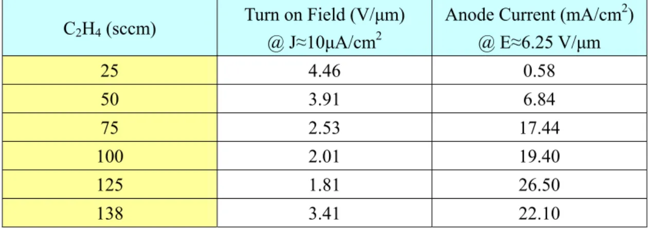
Figure 3.8 (a) J-E field emission characteristics of CNTs synthesized with different C2H4 flow rates and (b) the corresponding FN plot………...125
Figure 3.9 (a) Raman analysis of samples after CNT synthesis process conducted with different C2H4 flow rates and (b) the plot of ID/IG intensity vs. C2H4
flow rates………126 Figure 3.10 SEM images of surface morphologies of samples using multilayer
catalysts (20Co/30Ti/100Al) after CNT synthesis process conducted at different temperatures: (a) 700, (b) 650, (c) 600, (d) 550, (e) 500, (f) 450, (g) 400, and (h) 370℃. (The scale bars in the insets represent 2μm)………..………127 Figure 3.11 SEM images of surface morphologies of samples using single layer
catalyst (20Co) after CNT synthesis process conducted at different temperatures: (a) 700, (b) 650, and (c) 600℃. (The scale bars in the insets represent 2μm)……….129 Figure 3.12 Arrhenius plots for (a) the multilayer catalyst (20Co/30Ti/100Al) and (b)
the single layer catalyst (20Co)………..130
Chapter 4
Figure 4.1 Schematic diagrams showing the concept of beam overlapping………131 Figure 4.2 Schematic of the conventional gate structure: (a) top image and (b)
cross-sectional image……….132 Figure 4.3 The trajectories of electrons emitting from conventional triode devices
with different gate widths: (a) 30, (b) 60, (c) 120, (d) 240, (e) 480, and (f) 960 µm………...133 Figure 4.4 Spot sizes as a function of gate width in the conventional gate
Figure 4.5 Schematic of the focusing gate structure: (a) top image and (b) cross-sectional image……….135 Figure 4.6 The trajectories of electrons emitting from self-focusing gate devices with
different gate spacing: (a) 100, (b) 150, (c) 200, (d) 250, (e) 300, and (f) 350 µm………...136 Figure 4.7 Spot size as a function of gate spacing in the self-focusing gate
structure……….137 Figure 4.8 Schematic drawings for the process flows of the self-focusing gate
devices………138 Figure 4.9 SEM images of the self-focusing gate device: (a) top view and (b)
cross-sectional view………139 Figure 4.10 (a) HRTEM image of nanotubes grown with the multilayer catalyst at
500℃, and the inset is an enlarged partial image of the square region. (b) The correlative Raman spectrum of nanotubes………..……….140 Figure 4.11 (a) Field emission characteristics of conventional and self-focusing gate
devices and the inset shows the corresponding FN plot……….141 Figure 4.12 Photo-luminescent images of (a) the conventional and (b) the
self-focusing gate structure. The squares shown in the images are the corresponding region of CNT emitters of the field emission devices….142
Chapter 5
Figure 5.1 Schematic drawings for the process flows of the planar field emitters………143 Figure 5.2 SEM images of submicron gaps of planar field emitters with spacing of (a)
200 nm, (b) 300 nm, and (c) 500 nm………...144 Figure 5.3 The top-view SEM image of a planar field emitter and the schematic
diagram shown in the inset………..145 Figure 5.4 A schematic diagram of the field emission measurement of a planar field
emission diode……….146 Figure 5.5 (a) Field emission characteristics of planar edge field emission diodes of
different spacing between emitters and collectors and (b) the corresponding FN plot………147 Figure 5.6 Schematic drawings for the fabrication procedures of a quasi-planar field
emission diode……….148 Figure 5.7 (a) The cross-sectional and (b) top-view SEM images of a quasi-planar
field emission diode………149 Figure 5.8 SEM and AFM images showing the surface morphologies of Cr thin film
(a) before and (b) after the forming process, respectively……….150 Figure 5.9 A schematic diagram of the field emission measurement of a quasi-planar
field emission diode………151 Figure 5.10 (a) Field emission characteristics of quasi-planar field emission devices
with and without forming process; (b) the corresponding F-N plot of the formed device………..152 Figure 5.11 The field emission characteristics of quasi-planar devices with different
Chapter 1
Introduction
1.1 Overview of Vacuum Microelectronics
The emergence of vacuum tubes could trace back to the observation of emission current by the research team of Thomas Edison while they conducted the experiment of evacuated light bulb. The phenomenon that the filament in vacuum environment could induce emission current did not attract much attention because of no potential application until the invention of the vacuum tube diode by J. Ambrose Fleming in 1904. Afterward, the triode vacuum tube amplifier invented by Lee De Forest in 1906 launched the electronics industry since it marked the transition of the vacuum tube from a passive to an active device. With the combination of the control grid, the vacuum tube became the key element in the emerging discipline of electronics, especially for the radio stations, and the great quantity of requirement for vacuum tubes emerged in World War 1 owing to the military concern. In 1916, the tetrode, with an additional grid compared to triode, further made the remarkable advancement for the vacuum tube in the use of audio frequency power amplifier. In 1926, the pentrode tube, utilizing a third grid, was designed to overcome the problem of negative resistance characteristics caused by secondary emission from the anode being attracted to the positively charged screen in tetrode. The fact that the suppressor grid provided a means to prevent the secondary emissions from reaching the screen grid allowed the full capabilities of the vacuum tubes to be realized in the application of power amplifier. Despite its numerous applications in research and
communications, the vacuum tube had many drawbacks. It was extremely fragile, had a limited life, was fairly large, and required a lot of power to operate its heating element.
Recent development of vacuum microelectronics started in 1928, when R. H. Fowler and L. W. Nordheim published the theory of field emission, which described the relationship between the emission current density and the applied electric field based on electron tunneling through metal surfaces [1.1]. According to Fowler-Nordeim theory, a highly applied electric field of approximately 103 V/µm is necessary for electrons tunneling through the triangular barrier at the metal surfaces. Therefore, there was no remarkable advance in application until 1968, when C. A. Spindt published the work about a fabrication method to create small dimension metal cones by thin film vacuum deposition techniques [1.2]. Because of the outstanding properties of Spindt cathode, many researchers had devoted to the work on the refinement, characteristics, and applications of the Spindt emitters since the late 1960s.
In 1947, William Shockley, Walter Brattain, and John Bardeen successfully invented the first point-contact bipolar transistor in Bell Lab [1.3]. After that, the concepts of integrated circuits (ICs) subsequently proposed by Jack Kilby worked for Texas Instrument and Robert Noyce worked for Fairchild Semiconductor in 1960s. The invention of solid-state devices and concepts of ICs revealed the unpredictable potentials of solid-state electronics and, therefore, entered a new era [1.4-1.5]. In fact, “vacuum state” devices have potentially a number of outstanding advantages with respect to the presently much popular “solid state” devices, including fast drift velocity and associated transit time, radiation hardness and temperature insensitivity, and higher output power. For example, the saturation drift velocity is limited to less than 3×107 cm/sec in all solid-state devices whereas the saturation electron velocity in
vacuum is limited to 3×1010 cm/sec theoretically and practically to about 6-9×108 cm/sec [1.6]. The faster drift velocity of vacuum devices as compared with the solid-state devices results from less scattering in the channel of vacuum devices. Additionally, because there is no medium in the channel of vacuum devices, temporary and permanent radiation effects should be neglected and the effects of temperature on performance are essentially none exists. The comparisons between vacuum microelectronics and solid state devices are shown in Table 1.1.
Because of the surging worldwide interest in vacuum microelectronics and their applications, the first International Vacuum Microelectronics Conference (IVMC) was held in 1988 for the scopes providing a meeting for researches to gather and exchange information about all aspects of the field, including emission device physics, materials, and fabrication processes, etc. So far, much effort had been put into the work about improving the characteristics of emitters, such as lower operation voltages, higher emission current density, and longer lifetimes. Different cathode materials and device structures also have been proposed for further advancing the technology.
1.2 Theory of Field Emission
In semiconductor physics, the thermionic-field emission and field emission are both important mechanisms for the transport of electrons over the potential barrier between the metal and the semiconductor. In Schottky barriers on highly-doped silicon crystal, the depletion region is so narrow that the electrons can tunnel through the barrier near the top where the barrier is small enough which is called thermionic-field emission. On the other hand, in a degenerate silicon crystal, the electrons can tunnel through the energy barrier even near the Fermi level which is
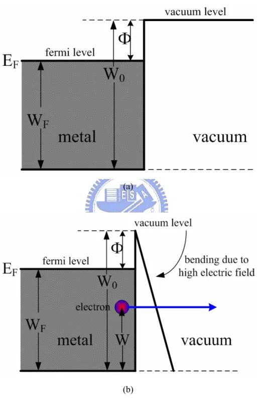
called field emission. It can be found that the tunneling in thermionic-field emission process requires electrons with higher energy than in field emission process. The emission of electrons from a surface of conductive material such as metal or semiconductor into a vacuum environment at an extremely high electric field is also a quantum mechanical tunneling phenomenon. The energy diagram of a metal-vacuum system without external electric field is displayed in Fig. 1.1(a). As shown in Fig. 1.1(b), the vacuum level is bent at extremely high electric field and the energy barrier between the surface of metal and the vacuum become so narrow that the electron can tunnel through it easily, even at very low temperature. Here W0 is the energy
difference between an electron at rest outside the metal and an electron at rest inside the metal, whereas WF is the energy difference between the Fermi level and the
bottom of conduction band. The work function Ф defined as Ф = W0- WF. When an
external electric field is applied, the vacuum level is reduced and the energy barrier at the surface of conductive metal or semiconductor becomes thinner. Then an electron having energy “W” has a finite probability of tunneling through the surface barrier. Fowler and Nordheim derive the famous Fowler-Noedhiem equation (1.1) as below [1.7-1.8]:
( )
( )
⎥⎥⎦ ⎤ ⎢ ⎢ ⎣ ⎡− = E y v b y t aE J 2 3 2 2 exp φ φ (1.1)where J is the current density (A/cm2), E is the applied electric field (V/cm), Φ is the work function (eV), a = 1.56×10⁻⁶, b = -6.831×10⁻⁷, y = 3.7947×10⁻⁴E1/2/Ф, t2(y)≒1.1 and v(y) can be approximated as [1.9]
(
y)
y v( )=cos 0.5π (1.2) or 2 95 . 0 ) (y y v = − (1.3)Substituting relationships of J = I/α and E = βV into Eq. 1.1, where α is the emitting area and β is the local field enhance factor at the emitting surface, following equation can be obtained ⎥ ⎥ ⎦ ⎤ ⎢ ⎢ ⎣ ⎡− = V y bv y t V A I β φ φ αβ 32 2 2 2 ( ) exp ) ( (1.4)
Then take the log. Form of Eq. 1.4
⎟ ⎟ ⎠ ⎞ ⎜ ⎜ ⎝ ⎛ × − ⎥ ⎦ ⎤ ⎢ ⎣ ⎡ × = ⎟ ⎠ ⎞ ⎜ ⎝ ⎛ − V y v y t V I β φ φ αβ ( ) 10 97 . 2 ) ( 10 54 . 1 log log 2 3 7 2 2 6 (1.5)
from Eq. 1.5, the slope of a Fowler-Nordhiem (F-N) plot is given by
) ( 10 97 . 2 2 3 7 β φ × = ≡slopeFN S (1.6)
The parameter β can be evaluated from the slope S of the measured F-N plot if the work function Ф is known
) ( 10 97 . 2 2 3 7 S φ β ≅− × (1.7)
Emission area α can be subsequently extracted from a rearrangement of Eq. 1.5
⎟ ⎟ ⎠ ⎞ ⎜ ⎜ ⎝ ⎛ × ⎟ ⎟ ⎠ ⎞ ⎜ ⎜ ⎝ ⎛ = × ⎟ ⎠ ⎞ ⎜ ⎝ ⎛ = − V V I β φ φ β φ α 2 3 7 2 6 2 10 53 . 6 exp 89 . 9 exp 10 4 . 1 (1.8)
For example, electric field at the surface of a spherical emitter of radius r concentric with a spherical anode (or gate) of radius (r + d) can be represented analytically by ⎟ ⎠ ⎞ ⎜ ⎝ ⎛ + = d d r r V E (1.9)
Though a realistic electric field in the emitter tip is more complicated than the equation above, we can multiple Eq. 1.9 by a geometric factor β’ to approximate the real condition.
⎟ ⎠ ⎞ ⎜ ⎝ ⎛ + = = d d r r V d r F Etip ( , ) β' (1.10)
Where r is the tip radius of emitter, d is the emitter-anode (gate) distance, β’ is a geometric correction factor [1.9], and F(r,d) is a function of r and d.
For a very sharp conical emitter tip, where d>>r, Etip approached to β’(V/r).
Moreover, for r>>d, Etip approaches to β’(V/d) which is the solution for parallel-plate
capacitor and for a diode operation in a small anode-to-cathode spacing.
As the tip radius of the gated field-emission array is very small, Eq. 1.10 can be approximated as: ) ( ' r V Etip =β (1.11)
Combining E=βV and Eq. 1.11, we can obtain the relationship:
) ( ' r V V Etip =β =β and β'=βr (1.12)
The tip radius r is usually in the range from a few nm to 50 nm, corresponding to the parameter β’ ranging from 10-1 to 10-2.
Besides, transconductance gm of a field emission device is defined as the change
in anode current due to a change in gate voltage [1.10].
ve m Vg Ic g ∂ ∂ = (1.13)
Transconductance of a field-emission device is a figure of merit that gives as an indication of the amount of current charge that can be accomplished by a given change in gate voltage. The transconductance can be increased by using multiple tips or by decreasing the cathode-to-gate spacing for a given cathode-to-anode spacing.
In past decades, vacuum electronic devices have been developed by reducing the device scale down to micro-size with the improved manufacturing technologies and equipments. Due to the outstanding properties of vacuum microelectronics, there are several potential applications attracting worldwide attention, including field-emission displays (FEDs) [1.11-1.15], microwave amplifiers and generators [1.16-1.18], ultra-fast switches, intense electron/ion sources [1.19-1.20], electron source of scanning electron microscope (SEM) and e-beam lithography, micro-sensors [1.21-1.22], and devices needed to work in hostile environment. Among these applications, FEDs seem most likely to have substantial commercial impact due to the emerging requirement in flat panel display industry.
1.4 Field Emission Displays
Owing to the requirement of displays with excellent image qualities and large image size, the development of flat-panel displays (FPDs) is one of the most important industries in the world now. Based on the operation physics of display devices, the flat panel displays generally can be categorized into two types: self-emissive and non-emissive types. The non-emissive type can not produce luminous light by itself, which should combine with other lighting elements for displaying images, such as active matrix-liquid crystal displays (AMLCD) which need a back light module. In contrast, the self-emissive type can produce graphic vision by itself, and there are many technologies announced worldwide, including plasma display panel (PDP), organic light Emission display (OLED), light emission diode (LED), polymer light emitting diode (PLED), electro-luminescence display (EL display), vacuum fluorescent display (VFD), Flat cathode-ray tube (CRT), and field
emission display (FED). Among these display technologies, FEDs were considered to be one of the most promising technologies that will be the major display technique in the near future due to its outstanding performance.
The idea of the field-emission display was first proposed and described in U.S. patent 3,500,102 issued in 1970 by Crost, Shoulders, and Zinn. However, the first monochrome prototype was demonstrated in Japan Display until 1986 by a group from LETI [1.23] and the first color display (6 inch) was demonstrated in 1993 by Pixel/LETI [1.24]. To know the history of field-emission displays better, more relative events of field-emission displays were listed in Table 1.2.
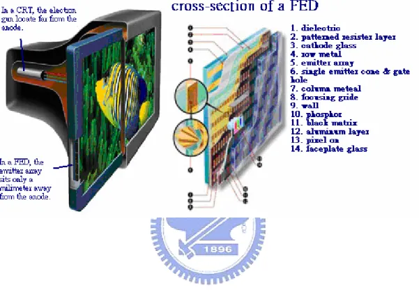
The operation of FED is similar to that of CRT, in which phosphor is excited by a stream of electrons traveling through a vacuum. In contrast with CRT which employed electron guns, FED is matrix-addressed by an array of emitters where electrons emitted to a phosphor anode plate that is located in close proximity (0.2-2 mm) to the cathode plate. It can provide an image with high resolution and avoid the distortion of image caused by external electric or magnetic field. The figures of field-emission displays and traditional CRTs shown in Fig. 1.2 illustrate the differences between these two displays schematically. The advantages of field-emission displays over other flat panel displays are higher brightness, better viewing angle, lower power consumption, less radiation, and larger operating range of temperature. The comparison of the characteristics for several flat-panel displays is listed in Table 1.3.
Generally, the field-emission displays could be classified into two main categories based on the operation configuration: diode and triode structures. As shown in Fig. 1.3(a), the field emission current is emitted from the cathode to the anode in the diode configuration, and the emission current is controlled by the voltage applied on the anode electrode. It has the merit of simple structure as compared with the
triode structure. However, the driving voltage required to show a grayscale is high so that it is costly and complex for the design of driving circuit. By comparison, the triode configuration, shown in Fig. 1.3(b), utilizes an extraction gate proximity to the emitter array so as to extract electrons from the cathode with a relative lower driving voltage. The emission current density from the cathodes to the anode is controlled by the voltage biased to the gate electrode. The electrons on the tip of emitters are extracted by the electric field induced from the gate voltage and parts of them are attracted by the electric field induced from the anode voltage. In the triode configuration, a much lower driving voltage is required to realize a grayscale than the diode structure. In addition, the field emission device with a triode structure has the merits of luminous efficiency, emission stability, and uniformity over large areas compared with diode one [1.25].
1.4.1 Technologies of Field Emission Displays
Fundamentally, FEDs are constructed by using three elemental technologies: micro-fabrication technology for the emitter arrays, optoelectronic technology for the anode plates, and vacuum technology for the packaging. Among these technologies, the performance of FEDs is determined by the technology of the cathode plates by which the electrons are generated. So far, researchers have put their attention to the development of new cathode structures for more robust in manufacture and application, such as Spindt-type field emitters, silicon tip field emitters, metal-insulator-metal (MIM), ballistic-electron surface-emitting device (BSD), ferroelectric emitters, and planar field emitters including surface conduction electron emitter (SCE) and edge field emitters. Besides, new cathode materials, such as diamond, diamond-like carbon, and carbon nanotubes, had been intensively studied for their potential as attractive electron sources. Many companies like Samsung of
Korea, ITRI of Taiwan, NEC of Japan, etc. have taken a lot of resources to research and develop the technology of field-emission display, and many amazing achievements had been announced in publications.
1.4.1.1 Cathode Structures
1.4.1.1.1 Spindt-Type Field Emitters
The original idea for the development of microfabricated field emitter array (FEA) came from Ken Shoulders and Dubley Buck at Massachusetts Institute of Technology (MIT) in the 1950s [1.26] but it was realized 40 years later beyond the reach of technology. The basic concepts were brought by Shoulders to the Stanford Research Institute (SRI) to develop the microfabricated vacuum integrated circuits [1.27] and he also proposed a thin display tube base on matrix-addressed arrays of microfabricated field emitters, the field-emission displays (FEDs) [1.28]. As part of Shoulder’s program, Capp Spindt proposed a smart method to form the arrays of miniature metal field emitter cones in microsize cavities with an surrounded extraction gate [1.29]. The cathodes of Spindt field emitter arrays are fabricated by forming metal cones on the conducting cathode electrodes as electron emitters by using thin film deposition processes. The metal cone is surrounded by an accelerating grid electrode (gate) which is insulated from the conducting cathode electrode by a dielectric layer. The cathode array features like a source of electrons with a positive voltage bias applied to the surrounding gate electrode. The micrographs of Spindt field emitter arrays taken by SEM are shown in Fig. 1.4 [1.27]. Although the Spindt type field emitter array provide a method to realize sharp metal tips with extraction gate electrode, it still has some drawbacks of needing huge metal depositing equipment, complex processes, requirement of high driving voltage, and reliability issues.
1.4.1.1.2 Silicon Tip Field Emitters
Sharp silicon tips of field emitter array are fabricated from crystalline silicon wafer by using oxidation processes to obtain silicon tips with small radius [1.30]. The processing steps of forming the silicon tips can be realized via standard semiconductor processes. According to some researches, the emission current from silicon tips can reach as high as 10 µA/tip [1.31]. Furthermore, crystalline silicon is a good material for the investigation of field emission array because of its great electronic, crystalline, mechanical properties, and availability. With well-developed techniques and equipments for fabrication, the apex radii of fabricated silicon tips can be bellow 10 nm with small deviation. One of the methods to form silicon tips is utilizing the orientation-dependant etching (ODE) which can form a convex pyramids structure [1.32-1.33]. Another way of fabricating silicon tips array is the oxidation sharpening process which is also the most used method in creating sharp tips on silicon wafers [1.34]. However, the array of silicon tips still has the problem of local failure due to high emission current density. Local heating at the silicon tips due to high emission current passing through can result in a local evaporation of silicon tips to reduce its sharpness and, therefore, cause a gradual degradation in emission current. Moreover, the requirement of driving voltage is still too high for the applications of field-emission devices due to its high work function.
1.4.1.1.3 Metal-Insulator-Metal Emitters (MIM)
Metal-insulator-metal cathodes are a kind of thin film tunneling device proposed by Mead in early 1960s and has been studied by many researchers [1.35-1.40]. Due to the stack structure, the buried cathode of MIM devices is less contamination and the electrons tunnel through interfacial Schottky barriers instead of surface barriers. This
device consists of a thin insulating film (e.g. Al2O3) sandwiched between two metal
electrodes, as shown in Fig. 1.5(a). The ultra-narrow insulating film allows the tunneling trough of electrons when a moderate electric field is applied across the layer. The energy diagram in Fig. 1.5(b) shows that the tunneling electrons are injected from the negative electrode (the emitter) through the insulating layer into the positive electrode (the gate) as hot electrons and are detected as diode current Ib. Part of the
electrons have sufficient kinetic energy to overcome the surface energy of the Au and emit into the vacuum, which are collected as an emission current Ie. However, most of
the tunneling electrons lose their kinetic energies while they pass through the structure due to scattering events in both the insulator and the gate metal. It is important to notice that the MIM structure requires a very precise control over the thickness of film to even atomic scale and the roughness of film is also very critical which can cause a very significant fluctuations in emission current and emission uniformity.
1.4.1.1.4 Ballistic Election Surface-Emitter Device (BSD)
In 1998, a novel cold-cathode technology based on a nanocrystallized polysilicon (NPS) layer was reported by the authors [1.41]. The electron emission characteristics strongly suggest that electrons injected into the NPS layer are transported quasi-ballistically [1.42]. It showed various excellent characteristics as compared with conventional FEDs [1.43] and it was termed a ballistic electron surface-emitting display (BSD). The device structure is schematically illustrated in Fig. 1.6. A non-doped polysilicon layer formed by a plasma-enhanced chemical vapor deposition (PECVD) technique was anodized in a solution of HF and ethanol under the illumination of tungsten lamp in order to form the NPS layer. After anodization, thin SiO2 layers on the surface of Si nanocrystallites were created by an electrochemical
stability and a frit sealed model was fabricated [1.44-1.45]. However, the oxide charging effect results in the degradation of device performance, and damage of thin oxide layer often takes place while the current density is large.
1.4.1.1.5 Ferroeletric Emitters
About 40 years ago, it has been observed that electrons emitted from the surfaces of ferroelectric materials during polarization reversal [1.46-1.47]. It was recognized that the polarization induces macroscopic charge separation on the two opposite surfaces of ferroelectric samples. As shown in Fig. 1.7, the screening charges are developed to compensate the net charges. A fast reversal (about sub-microseconds) of the polarization results a large electric field that ejects the electrons from the negative charged surface. By contrast, no external extraction field is required to overcome the surface work function to obtain electrons emission from ferroelectric emitters [1.48]. The emission depends on the polarization fields within the ferroelectric material and only excitation energies such as electrical, optical, thermal or mechanical energies are required to overcome the coercive fields. Ferroelectric emission is thus a transient unipolar effect generated from non-equilibrium charged ferroelectric surface. Ferroelectric cathodes have very robust surfaces that may be exposed to air and operated in poor vacuum conditions (up to 10-2 torr) or even in plasma. However, many issues in ferroelectric emissions such as polarization fatigue during multiple fast switching, emission current stability, and domain structure aging are still needed to be overcome before those envisioned devices could be realized.
1.4.1.1.6 Planar (Lateral) Field Emitters
Planar field emitters, small in device size, had the merits of design versatility and low operation voltage, and therefore showed a potential in vacuum microelectronics,
especially, for high frequency application. Besides, owing to the simplicity in device structure and operation in low voltage, the planar also attract much interest in the application of field emission displays, such as surface conduction electron emitter (SCE) and edge field emitters.
Surface Conduction Electron Emitters (SCE)
Surface conduction emission is the phenomenon that electrons are emitted from a cathode when electric current flows through the cathode in parallel with the cathode surface [1.49]. It has attracted a great deal of attention since a 10-inch full color display incorporated a thin film PdO cathode based on the surface conduction emission mechanism was built by the researchers at Canon in Japan [1.50]. The device structure with two ultrafine PdO film as cathode and gate electrodes from top view is demonstrated in Fig. 1.8(a). The forming process of the gap between cathode and gate electrodes is to apply a voltage between two electrodes so that an electric current with high density flows through the PdO film in parallel with the surface. The thin film generates Joule heating when the electric current passing through and cause a fissure of nano scale between two electrodes. The fissure where be spatially discontinuous but electric continuous which causes field emissions because of high fields established across the cracks along the surface. The emitted electrons can be collected by the anode spaced apart from the surface of cathode after multiple scatterings on the cathode, as shown in Fig. 1.8(b). Due to the nanosize of the gap between cathodes and gates, the driving voltage can be greatly suppressed to several decades volt. The uniformity of emission current from device to device is also good resulting from the uniform PdO film. However, the emission current from cathode to anode is still low due to the fact that most of the emitted electrons are collected by the gate electrode merely 10 nm apart from the cathode.
Thin Film Edge Emitters
In contrast to SCE formed by thick film techniques, the thin film edge emitters were fabricated mainly based on the thin film deposition process. Similar to the device structure of SCE, the emitter and collector electrodes were posited in the same horizon between which a submicron gap was created. So far, many techniques such as electron beam lithography (EBL), focus ion beam (FIB), and chemical mechanical polish (CMP) [1.51-1.53], were employed to form a small spacing across electrodes. Nevertheless, the throughput is poor and there is a lack of scalability for large area.
1.4.1.2 Cathode Materials
Fabricating field emission cathodes with low operation voltage, high emission current, excellent stability and good reliability is crucial to commercialize the field emission display. According to the F-N equation, the performance of emission devices could be improved with novel cathode materials in terms of aspects: the work function φ of the cathode material must be as low as possible and the field-enhancement factor β and emission area α should be as large as possible.
1.4.1.2.1 Diamond and Diamond-Like Carbon (DLC)
Diamond is one of the main crystalline allotropes of carbon, which is formed in an sp3 tetrahedral bonded cubic structure. Due to its negative work function, diamond possesses a very small barrier for its electrons to leave the surface and emit into the vacuum environment. When the surfaces of diamond are terminated with hydrogen atoms, the electron affinity, which is a measured energy barrier that electrons must overcome to escape from the surfaces of diamond into vacuum, can become negative
[1.54]. Moreover, the diamond surfaces are chemically inert and mechanically strong. Therefore, diamond is considered a very promising material of the electron emitters in vacuum microelectronics. Unfortunately, the conductivity of diamond is not good, and thus the maximum emission current from the diamond surface to the vacuum environment is limited. Additionally, the process temperature for diamond to be deposited via chemical vapor deposition is also usually higher than 700 °C. It makes the diamond electron emitters difficult to be fabricated on the glass substrates.
Diamond-like carbon (DLC) is another particular interesting material of three dimensional network of sp3 and sp2 bonded carbon atoms [1.55-1.57]. For its good field emission properties and lower deposition temperature than diamond, DLC attracted a lot of interesting from many researches. Depending on the deposition conditions, the ratio of hydrogen carbon (a-C:H) and hydrogen-free carbon (a-C) can be altered in the DLC. It also means that different portions of sp3 and sp2 bonding can be achieved to dictate the field emission properties [1.58-1.59]. It is interesting that the emission properties of these amorphous carbon or DLC improve with increasing sp3 content, while those of diamond materials deteriorate. It suggests that there is an optimal ratio of sp3 and sp2 bonding in order to obtain emitters with lowest turn-on field. However, the process of synthesizing the DLC is complex and sensitive to the growth conditions. In addition, the emission site density of DLC is poor for the application in FEDs.
1.4.1.2.2 Carbon Nanotubes
Carbon nanotubes had attracted a great deal of attention since its first observation in 1991 by Iijima [1.60]. Generally, they can be classified into single-walled nanotubes (SWNTs) and multi-walled nanotubes (MWNTs) depending on their fine structures. Due to their high aspect ratio, strong mechanical strength, good thermal
conductivity, and inert chemical properties, CNTs are recognized as a very promising material of electron emitters. From the report of De Heer, the emission current density over 100 mA/cm2 is measured from a partially aligned CNTs film prepared by drawing nanotube suspensions through 200 nm pore ceramic filters [1.61]. It has also been reported in many other researches that CNTs can provide a high emission current density [1.62-1.63].
So far, most nanotubes could be synthesized via three techniques, including arc discharge [1.64], laser ablation [1.65], and chemical vapor deposition (CVD) [1.66]. The arc discharge system employed two carbon electrodes kept in a close distance in helium (He) ambience for igniting the phenomenon of arc discharging, and thus CNTs could be grown inside the cathode electrode with the aids of carbon source evaporated form anode electrode. The CNTs synthesized by using arc discharge are usually in bundles and need to be released by ultrasonic cleaner and particular etching solution. The laser ablation system applied a laser source to vaporize a graphite target in a chamber, and small carbon molecules or atoms condense quickly to form large clusters and then react with the catalyst to form CNTs as the vaporized graphite cooled rapidly. However, the arc discharge and laser ablation systems have the drawbacks of high thermal budget, low throughput, and non-uniformity in synthesis. In contrast, CVD system appears to be a good technique in synthesis of CNTs for its simplicity and scalability. The process of synthesizing CNTs in chemical vapor deposition system includes heating a catalytic material at high temperature and flowing hydrocarbon gas through the reacting chamber for a period of time. With the aids of catalytic particles of transition metals, such as iron (Fe), nickel (Ni), or cobalt (Co), the carbon atoms precipitate from the super-saturated nanoparticles and form tubular carbon solids in sp2 bonding. Therefore, recently many researchers have devoted themselves to the development of CVD techniques for synthesis of CNTs in
pure quality and high quantity.
1.5 Motivation
For the application of flat panel displays, large-area and cost-effective manufacture processes are essential for the profits of manufacturers. Glasses, naturally containing silica as a main component, could provide sufficient mechanical strength for fabrication processes, and seems to be a good candidate for supporting substrates. However, the softening point of glasses is about 580℃, which limits the fabrication processes that should be carefully designed so as to eliminate the issues of bending or cracking.
Carbon nanotubes (CNTs) having superior properties, such as high aspect ratio, high thermal and electrical conductivity, and chemical inertness, have been considered as potential cathode materials for field emission. Nowadays, nanotubes can be synthesized via three methods, including arc discharging, laser ablation, and chemical vapor depositions (CVD). The former two methods could not directly form nanotubes on the glass substrates due to their high temperature processes and poor uniformity. Therefore, CVD, which can directly and selectively grow nanotubes at designate area, is supposed to be a promising technique for the application of CNT-FEDs in large area. Current CVD systems could be divided into two categories: plasma-based CVD, and thermal CVD (t-CVD). The plasma-based CVD, including PECVD, MPCVD, and ECR-CVD, must be consisted of a vacuum environment for igniting and sustaining the plasma, and therefore the instruments is complex and costly in design. On the other hand, the thermal CVD system could be operated at atmospheric ambient, that is, cost effective and higher throughput. However, as compared with PECVD, t-CVD
could not provide sufficient growth rates of nanotubes at low temperatures because of the low reactivity of processing gases. Thus, the substrate typically was required to heated up to higher temperatures approximately 600℃ or more to effectively synthesize nanotubes in thermal CVD system. Such high temperatures were not compatible with temperature-sensitive processes and materials, preventing the utilization of glass substrate. Therefore, we employ multilayer catalysts to provide high catalytic activity for synthesis of nanotubes at low temperatures in thermal CVD system and investigate the correlative growth mechanism. Furthermore, the morphologies and field emission characteristics are also improved by modifying process conditions comprising different flow rate ratios of reaction gases.
Because lower turn-on voltage is necessary to reduce the cost of driving circuits of field emission displays, the triode devices fabricated with an extraction interposed between cathode and anode plates is demonstrated to be an essential technique for realizing commercial products. Nevertheless, the divergence of electron beams is a serious problem as the field emission devices operate in triode configuration. For large distances that are generally necessary to avoid arcing phenomenon as phosphors are biased with high operation voltages at anode plates for high luminescent efficiency, the electron beams are easily spreading and cause inevitable cross-talking noises between neighboring pixels. Therefore, much effort has been made to introduce the focusing electrodes which are negatively biased with respect to the extraction gates for modifying the electrical potential around the emitters so as to control and focus the trajectory of the emitting electrons. These focusing electrodes utilized in combination with the triode structure gave rise to an increasing cost due to the complexity in manufacturing processes. In order to simplify the manufacture process, a new mechanism for controlling the beam trajectory is proposed, and the focusing structure was fabricated to characterize the device performance.
Additionally, planar field emitters have the low driving voltages as compared with other cathode structures due to the sub-micron spacing between emitters and collectors. Moreover, the device structure is simple and possesses the advantages in design versatility. However, most of planar field emitters are manufactured with complex processes, such as creation of sub-micron gaps via focus ion beam (FIB), or via electron beam lithography (EBL). Thus the throughput of fabrication is low, and the application is limited as well. For obviating the issue mentioned above, two kinds of manufacture processes are proposed for simplicity in fabrication of high performance planar field emitters.
1.6 Thesis Organization
In chapter 1, the overview of vacuum microelectronics and basic theory of field emission were first introduced. A description about the field emission displays and their cathode technologies were briefly addressed in following sections. Finally, the motivation of this thesis was mentioned before the thesis organization.
Chapter 2 shows the synthesis of nanotubes at low temperatures via atmospheric thermal CVD system in combination with multi-layered catalysts, and the functionality of different components in the catalysts is also discussed in this chapter.
In chapter 3, the field emission characteristics of nanotubes synthesized with multi-layered catalysts is improved by modifying the ratios of flow rates of the reaction gases.
Chapter 4 discloses a novel self-focusing gate structure and related processes, which could resolve the issue of electron beam spreading as the FEDs operate in triode configuration.
In chapter 5, a simple fabrication process consisting of wet etching and lift-off is proposed to create a submicron gap for planar edge emitters. Additionally, a quasi-planar structure of submicron gaps controlled via thin film deposition process is also demonstrated, and the field emission characteristics are further improved by a forming process so as to reduce the operation voltages.
Finally, the conclusions and recommendations for future research are described in chapter 6 and 7, respectively.
Chapter 2
Investigation of Carbon Nanotubes
Synthesized at Low Temperatures Using
Multi-layered Catalytic Films
In this chapter, carbon nanotubes were synthesized at 550℃ using multilayer catalysts which were composed of supporting layer, interlayer, and catalytic metal. Supporting layer could effectively enhance the dispersion of catalytic nanoparticles and meanwhile avoid their agglomeration during the synthetic process. Interlayers not only promoted the distribution of nanoparticles but also function to enhance the precipitation of carbon atoms. Interlayers which had surface energy comparable to catalytic metal and positive of formation heat of carbide revealed to improve the growth of CNTs at low temperatures.
2.1 Introduction
Carbon nanotubes (CNTs), discovered by Iijima in 1991 [2.1], are promising candidates for emitter materials of cold cathodes due to their unique properties, such as high aspect ratio, high mechanical strength, chemical inertness and large current capability [2.2-2.4]. Wang et al. reported a low turn-on electric field of 0.8 V/µm from nanotube bundle emitters [2.5]; meanwhile, Zhu et al. demonstrated a very high current density of 4 A/cm2 from CNT field emitters [2.6]. In addition, Samsung
announced a matrix-addressable diode display using CNTs as emitters, showing the potential for field emission displays (FEDs) [2.7]. Therefore, field emission displays based on CNTs have attracted much attention in recent years [2.8-2.10]. For FEDs to be cost competitive with existing display technologies, inexpensive glass is commonly used as the substrates. Nowadays, several methods have been well developed for preparing CNTs on glass substrates at low temperatures, including screen printing [2.11], electrophoresis [2.12], and chemical vapor deposition (CVD) [2.13-2.17]. Among these methods, CVD appears to be a superior one due to its good uniformity and pixel resolution. Numerous CVD systems have been employed to directly grow CNTs on glass substrates, and they can be categorized into two types of instruments based on the ways by which the hydrocarbon gases are decomposed: plasma-based CVD and thermal CVD. The plasma-based CVD systems, such as inductively coupled plasma CVD (ICP-CVD) [2.13], electron cyclotron resonance CVD (ECR-CVD) [2.14], and plasma-enhanced chemical vapor deposition (PECVD) [2.15], utilize a source of plasma to effectively decompose the hydrocarbon gases, thus enhancing the growth of nanotubes at low temperatures on glass substrates. In contrast, thermal CVD [2.16-2.17] imply that the decomposition of reaction gases is carried out with the aid of thermal energy supplied by the instrument. For the sake of different operation mechanism, the plasma-based systems revealed to be a better choice than thermal one due to the higher efficiency in synthesis of CNTs. It has been shown that the activation energy characterized for the growth of CNTs by PECVD was lower than that by thermal CVD [2.18-2.19] and that the growth limiting step was determined by the diffusion of carbon on catalysts: surface diffusion for PECVD and bulk diffusion for thermal CVD [2.20]. This indicates that effective decomposition of carbon precursors by plasma could enhance the growth rates at low temperatures due to a lower activation energy. Nevertheless, it is worth mentioning that a vacuum
environment is necessary for the purpose to ignite and sustain the plasma source. Thus an evacuation system should be equipped in plasma-based systems, that is, a higher cost for large area and low throughput. Moreover, it is not easy to well control the plasma source in large area because the parameters for sustaining plasma should be precisely provided to obviate a big issue in non-uniformity. Therefore, it is generally suggested that thermal CVD would be a favored method owing to its controllability and scalability. Despite the high feasibility, however, thermal CVD typically involves processing temperatures of over 600 to overcome the decomposition energy of ℃ carbon precursors, which is significantly higher than the softening point of glass substrates (580 ). Thus, in several studies, a two℃ -zone electric furnace has been employed, which consists of a high temperature zone for preheating the reaction gas to enhance its reactivity [2.21-2.23], hence facilitating the growth of CNTs at low temperatures. With the similar ideas, there were work employing hot filament assisted systems [2.24], which consisted of a filament heated at high temperatures (~1600 ), ℃ to pre-decompose the precursors. These techniques are not only complicated in the manufacturing processes but also thermally inefficient because of the high thermal budget.
According to work published, the type of catalyst also plays an important role in the growth of CNTs because the process is a catalytic reaction. Kamada et al. indicated that a binary catalyst could synthesize CNTs well at low temperatures due to its high activity [2.25]. Park and coworkers also employed a ternary alloy as a catalyst for improving the crystallinity of CNTs synthesized at low temperatures [2.16-2.17]. Since thermal CVD utilizes thermal energy to assist the decomposition of carbon precursors, a highly active catalyst is essential for low-temperature synthesis of CNTs. However, it is difficult to prepare these catalysts because the composition of elements should be carefully synthesized. In this chapter, multilayer catalysts were employed to