國 立 交 通 大 學
電子工程學系 電子研究所碩士班
碩 士 論 文
一個九位元,每秒八十百萬次取樣
低功率管線式類比數位轉換器
A 9bit, 80MS/s Low Power
Pipelined Analog to Digital Converter
研 究 生:賴宗裕
指導教授:陳巍仁 教授
低功率管線式類比數位轉換器
A 9bit, 80MS/s Low Power Pipelined Analog to Digital Converter
研 究 生:賴宗裕 Student:Tsung-Yu Lai
指導教授:陳巍仁 Advisor:Wei-Zen Chen
國 立 交 通 大 學
電 子 工 程 系
碩 士 論 文
A ThesisSubmitted to Department of Computer and Information Science College of Electrical Engineering and Computer Science
National Chiao Tung University in partial Fulfillment of the Requirements
for the Degree of Master
in
Electronics Engineering
December 2007
低功率管線式類比數位轉換器
學生:賴宗裕
指導教授
:陳巍仁
國立交通大學電子工程學系﹙研究所﹚碩士班
摘
要
管線式類比數位轉換器具有高速及中高解析度的特性,因此為可攜式電子產品中經常使用 之架構。其可藉由低電壓及功率最佳化設計,降低電路整體功率消耗。然而,在低電壓的操作 環境下, 由於信號的動態範圍減少, 電路的非理想效應會進一步劣化管線式類比數位轉換器的 性能,包含飄移電壓、運算放大器的非線性增益及電容的不匹配等效應造成之增益誤差。至今, 文獻上有許多校正電路技術發表, 其可藉由離線或背景補償等方式, 提升轉換器電路之性能。 本論文提出一個 1 伏特, 9 位元之管線式類比數位轉換器。 為改善低電壓操做運算放大 器之增益與頻寬, 本論文提出轉導分離式運算放大器電路, 其在相同之功率消耗與單位增益頻 寬之下, 可提升增益達 10 dB。此外, 為克服低電壓操做運算放大器之有限增益效應, 本架構 內含運算放大器及倍乘數位類比轉換器(M-DAC) 之增益萃取電路, 本論文並提出偏移誤差補 償方法, 以大達幅提高運算放大器增益萃取之準確性, 藉由離線補償可提升整體轉換器之有效 位元數達2 位元。 本實驗晶片以0.18μm CMOS 製程實作完成, 晶片面積為 1.45×1.55 mm2。本電路採用雙 重取樣技術以提升運算放大器之使用效率, 同時倍增取樣率, 其轉換率可達每秒八十百萬次取 樣。量測結果顯示其微分和積分非線性誤差(Differential and Integral Nonlinearity)分別為 +1.1/-0.8LSB和+1.3/-1.3LSB。 本轉換器之核心電路皆操作在 1 伏特工作電壓, 整體功率消耗 為 11.5mW, 其 FOM值達 0.88pJ/conversion。
A 9bit, 80MS/s Low Power
Pipelined Analog to Digital Converter
student:Tsung-Yu Lai
Advisors:Wei-Zen Chen
Department of Electronics Engineering National Chiao Tung University
ABSTRACT
Pipelined ADCs are widely applied in portable electronic devices thanks to its features of high speed operation and medium to high resolution in data conversion. Its power dissipation can be further reduced by applying low voltage and power scaling techniques. However, the dynamic range of the input signal is severely limited under a low supply voltage. The non-idealities of the data converter, such as offset voltage and gain error caused by OP gain nonlinearities and capacitor mismatches, will further degrade its overall performance. Nowadays, several calibration techniques have been proposed in the literature. The performance of the data converter can be enhanced by means of off-line or background calibrations.
This thesis proposes a 1 V, 9bits pipelined ADC. In order to improve the gain bandwidth performance of the operational amplifier under a low supply voltage, a novel OPAMP with split transconductance input stage is proposed. It can boost the conversion gain by 10dB under a given current consumption and without degrading its unity-gain bandwidth performance. Besides, in order to eliminate the OP finite gain effect under a 1 V supply, on-chip calibration circuits are incorporated to extract the conversion gain of the OP and MDAC. Furthermore, input offset cancellation techniques are proposed to improve the accuracy of the calibration circuits. The effective number of bits (ENOB) of the data converter can be improved by 2 bits by applying offline calibration.
V supply, and the total power consumption is 11.5 mW. The corresponding FOM (Figure of Merit) is 0.88pJ/conversion.
碩士班二年多來,我對於自己的成長感到滿意。很感謝陳巍仁老師的指導,也謝謝 307 及 319 實驗室所給予的資源,使我在學術上有十足的進步。當然,除了學術外,謝謝二位在當 兵的室友,也很謝謝在交大所認識的朋友們,包括 307 曾經指導過我的學長、527 一起打拚的 同學、520 一群歡笑的學弟們,很抱歉沒有細數你們的名字,但真的由衷感謝你們讓我有這麼 快樂的回憶。松諭、巧伶及黃董,請你們繼續努力,相信你們以後一定成就非凡,祝福你們! 最後,謝謝女友、老爸、老媽,謝謝老天爺,我畢業了! 賴宗裕 2008,1,3
國 立 交 通 大 學
電子工程學系 電子研究所碩士班
碩 士 論 文
一個九位元,每秒八十百萬次取樣
低功率管線式類比數位轉換器
A 9bit, 80MS/s Low Power
Pipelined Analog to Digital Converter
研 究 生:賴宗裕
指導教授:陳巍仁 教授
Contents
INTRODUCTION...1
1.1 Motivation ...1
1.2 Thesis Organization...2
CHAPTER 2...4
NYQUIST RATE DATA CONVERTER ...4
2.1 Introduction ...4
2.2 ADC Performance Metrics ...4
2.2.1 Resolution ...4
2.2.2 Signal-to-Noise Ratio (SNR)...5
2.2.3 Spurious Free Dynamic Range (SFDR) and Signal to Noise Distortion Ratio (SNDR)...7
2.2.4 Dynamic Range(DR) ...8
2.2.5 Imperfections ...9
2.2.6 Differential Non-Linearity (DNL) and Integral Non-Linearity (INL)...10
2.3 Review of ADC Architecture... 11
2.3.1 Flash ADC ... 11
2.3.2 Cyclic ADC...13
2.3.3 Pipelined ADC...13
2.4 Design Issue of Pipelined ADC ...16
2.4.1 Stage Accuracy and Speed Requirement ...16
2.4.2 Double Sampling ...18
2.4.3 Power Optimization...18
2.5 MATLAB Behavior Model ...19
CHAPTER 3...22
CIRCUIT SPECIFICATION...22
AND ...22
SIMULAION...22
3.1 Time-interleaved Pipelined ADC Design...22
3.1.1 Design Issue...22
3.1.2 Architecture ...23
3.2 Each Block of Pipelined ADC...24
3.2.1 Operational Amplifier...24
3.2.2 Common Mode Feedback Cicruit (CMFB) ...27
3.2.3 Comparator ...29
3.2.4 The 1.5 bit flash ADC ...31
3.2.6 Bootstrapped Switch...35
3.2.7 Multiply DAC (MDAC)...37
3.2.8 Double Sampling ...38
3.2.9 Final 2bit flash ADC...39
3.2.10 Clock Generator ...40 3.2.11 Timing Diagram...41 CHAPTER 4...43 CALIBRATION CIRCUIT ...43 4.1 Calibration Conception...43 4.1.1 Nonlinearity of gain...44 4.2 Calibration Circuit ...46
4.3 Operation Amplifier in Calibration Circuit...47
4.4 Calibration Circuit with Offset Cancellation...49
4.5 Simulation Result...52
CHAPTER 5...54
EXPERIMENTAL RESULT...54
5.1 Floor-planning and Layout...54
5.2 System Simulation Result ...55
5.2.1 Time domain Simulation ...55
5.2.2 Dynamic Simulation ...55 5.2.3 INL and DNL ...59 5.2.4 Dynamic Range ...60 5.2.5 Specification Table...61 5.3 Experimental Result...62 5.3.1 Measurement Consideration...62 5.3.2 Experimental Result...63 CHAPTER 6...68 CONCLUSION ...68 REFERENCE ...70
List of Tables
Table 3.1 OP pre-simulation and post-simulation result ...27Table 3.2 OP specification in 1st FADAC and 2nd MDAC ...27
Table 3.3 Mismatch parameter ...31
Table 4.1 Amplifier in calibration circuit simulated result...48
Table 5.1 ADC specification of pre-simulation and post-simulation ...62
Table 6.1 Performance summary of ADC at room temperature ...68
List of Figures
Figure 1.1 Applications of analog to digital converters ...1Figure 1.2 Survey of ADC Figure-of-Merit 1999-2006 ...2
Figure 2.1 (a) Transfer characteristic curve (b) Quantization error...5
Figure 2.2 (a) Quantizer model...6
(b) The probability density function of the quantization error ...6
Figure 2.3 Example of frequency domain plot...8
Figure 2.4 SNR versus input level...9
Figure 2.5 Imperfections in ADC (a) Offset (b) Gain error (c) Non-linearity...10
Figure 2.6 DNL and INL ... 11
Figure 2.7 Flash ADC architecture...12
Figure 2.8 Cyclic ADC architecture ...13
Figure 2.9 Pipelined ADC architecture...14
Figure 2.11 (a) Ideal transfer curve (b) With comparator offset...15
(c) With amplifier offset (d) With gain error ...15
Figure 2.12 (a) MDAC in sample mode (b) MDAC in hold mode ...17
Figure 2.14 (a) FADAC in hold mode (b) MDAC in hold mode ...20
Figure 2.15 Simulation result of Behavior model ...21
(a)With calibration (b)Without calibration ...21
Figure 2.16 (a)Gain versus ENOB (b)Gain versus Improvement ...21
Figure 3.1 Pipelined ADC and calibration circuit architecture ...23
Figure 3.2 (a) One stage opamp schematic...25
(b) Proposed opamp schematic...25
Figure 3.3 Proposed operational amplifier simulation result ...26
(a) Gain and phase response (b) Output linear range ...26
Figure 3.4 CMFB circuit (a) Conventional CMFB (b) Modify CMFB ...28
Figure 3.5 (a) Comparator schematic (b) Comparator simulated result...30
Figure 3.6 (a) 500 times Monte Carlo simulation ...31
(b) Times of Monte Carlo simulation and offset value relation ...31
Figure 3.7 1.5bit flash ADC schematic ...32
Figure 3.8 FADAC schematic ...34
Figure 3.9 (a) FADAC input sampling circuit (b) Clock waveform ...35
Figure 3.10 Bootstrapped switch schematic...35
Figure 3.11 (a) Circuit to simulate SFDR of bootstrapped switch ...36
(b) Dynamic simulation with different input frequency...36
(c) SFDR is 78dB when input frequency is 40MS/s and switch clock rate is 80MS/s ...36
(d) Time domain simulation ...36
Figure 3.12 MDAC schematic...38
(a) During Clk1 (b) During Clk2 (c) Clock waveform (d) INL plot...38
Figure 3.13 Double sampling ...39
(a )During Clk1 (b) During Clk2 (c) During Clkrst (d) Clock waveform ...39
Figure 3.14 2bit flash ADC ...40
(a) True table (b) Gate level implement (c) Simulation waveform ...40
Figure 3.15 (a) clock generatior schematic ...41
(a) waveform diagram (c) simulation resolutoin ...41
Figure 3.16 Timing diagram...42
Figure 4.1 (a) Ideal and real transfer curves...43
(b) FADAC in hold mode (c) MDAC in hold mode...43
Figure 4.2 Slope deviation due to gain deviation ...45
Figure 4.3 Nonlinearity of opamp versus differential output ...45
Figure 4.4 (a) Calibration circuit (b) Clock and output waveform...46
Figure 4.5 Illustration of off-line calibration operation...47
Figure 4.6 (a) Amplifier in calibration circuit (b) Bias circuit ...48
Figure 4.7 (a) Calibration circuit with offset...49
(b) VOS1 affection (c) VOS2 affection (d) VOS3 affection ...49
Figure 4.8 (a) VOS1 cancellation circuit (b) Waveform representation ...50
Figure 4.9 (a) VOS2 cancellation circuit (b) Waveform representation ...51
Figure 4.10 (a) VOS3 cancellation circuit (b) Waveform representation ...52
Figure 4.11 Calibration circuit simulation result...53
(a) Pre-simulation (b) Post-simulation ...53
Figure 5.1 Floor-planning and layout ...54
Figure 5.2 (a) Input waveform (b) Reconstructed output waveform...55
Figure 5.3 Simulated FFT in input frequency=8MHz,...56
Sampling rate=80MS/s ...56
(a) Pre-simulation and calibration OFF (b) Pre-simulation and calibration ON ...56
(c) Post-simulation and calibration OFF (d) Post-simulation and calibration ON ...56
Figure 5.4 Post-simulated ENOB vs. sampling frequency...57
Figure 5.5 Improvement vs. calibration output digital code with calibration ON...57
(b) Post-simulation of SFDR, SNDR, and ENOB vs input frequency...58
Figure 5.7 Corner of post-layout simulation ...59
(a) Sampling frequency is 80MS/s in TT and FF corners ...59
(b) Sampling frequency is 60MS/s in SS corner ...59
Figure 5.8 INL and DNL ...60
Figure 5.9 Dynamic range ...61
Figure 5.10 Measurement consideration ...63
Figure 5.11 ADC chip microphotograph...63
Figure 5.12 The measured calibration circuit output...64
Figure 5.13 Measured DNL and INL at 80MS/s with calibration off. ...64
Figure 5.14 Measured DNL and INL at 80MS/s with calibration on. ...65
Figure 5.15 Measured output FFT spectra...66
The 600mVPP 1MHz differential sinusoidal input is sampled at 80 MS/s. ...66
Figure 5.16 Measured SFDR,SNDR, and ENOB versus sinusoidal input is sampled at ...66
80 MS/s...66
Figure 5.17 Measured SNDR and SNR versus input level. The 1MHz differential sinusoidal input is sampled at 80 MS/s ...66
Figure 5.18 Measured SNDR and SNR versus input level. The 1MHz differential sinusoidal input is sampled at 80 MS/s ...67
C
HAPTER
1
I
NTRODUCTION
1.1 Motivation
Figure 1.1 Applications of analog to digital converters
Many of the communication systems today utilize the digital signal processing to resolve the transmitted information. Therefore, between the received analog signal and the DSP system, an analog-to-digital interface is required. This interface achieves the digitization of the received waveform subject to a sampling rate requirement of the system. Being a part of communication system, the A/D interface also needs to adhere to the low power constraint. Figure 1.2[1] shows the surveys of ADC from 1999 to 2006. The figure-of-merit (FOM) is expressed as 2ENOB Power FOM Conversion rate = × (1.1)
where ENOB means effective number of bit. State-of-the-Art for ADC design is approximately 1-picoJoule per conversion step.
Figure 1.2 Survey of ADC Figure-of-Merit 1999-2006
Among many types of CMOS ADC architectures, a pipelined architecture can achieve good high input frequency dynamic performances and as a high throughput. Low-power small-area ADCs with 10bit resolution and several tens of MS/s sampling rate are considered to be one of the significant components in battery-operated commercial applications including data communication and image signal-processing systems.
In this research, it is expected to suppress the power consumption so as to use 1.0 V power supply in analog circuit. A 9-bit 80MS/s pipelined A/D converter with off-line calibration has been designed and implemented with standard TSMC 0.18μm CMOS 1P6M process.
1.2 Thesis Organization
This thesis is organized into six chapters. In Chapter 1, this thesis is briefly introduced. Chapter 2 begins with the concepts of analog-to-digital conversion and performance metrics used to characterize ADCs. Then, the architecture of pipelined ADC is reviewed. The pipelined architecture is described in detail from its basic operation to the actual implementation of each pipelined stage. The 1.5-bit architecture with accuracy and speed requirement are pointed out. The affection of gain error in low voltage ADC and calibration
technique are also discussed in detail. Finally, the behavioral level simulations of a pipelined ADC are built by MATLAB so as to obtain the specification of design.
Chapter 3 describes the design issues of each block. The key circuit blocks used in the low-voltage ADC is presented. Among them are the proposed operational amplifier, the dynamic common mode feedback, the comparator, the FADAC and the clock generator. Then, transistor level simulated results of each circuit are shown.
Chapter 4 describes the calibration circuit which is constructed by SAR (Successive Approximation) architecture. The goal is to calculate the gain error in pipelined ADC which is described in chapter 3. By the output digital code, off-line calibration can boost the efficiency of pipelined ADC.
Chapter 5 shows the experimental results, including the chip layout, system simulation result, and measurement consideration. Following the experimental test results for the low-voltage pipelined ADC described in Chapter 3 and Chapter 4 and fabricated in a standard TSMC 0.18μm CMOS technology are summarized.
The conclusions of this work are summarized in Chapter 6. Following additional areas of researches are suggested and recommendations for the future work.
C
HAPTER
2
N
YQUIST
R
ATE
D
ATA
C
ONVERTER
2.1 Introduction
In this chapter, the first describes the concept of analog to digital conversions and discusses performance metrics to characterize ADCs. The second reviews some analog-to-digital converter (ADC) architectures, including flash ADC, cyclic ADC, and pipelined ADC. The fundamental issues in this design will be reviewed. Among them we focus on Nyquist rate pipelined ADC architecture. The third focuses on key building blocks in pipelined analog-to-digital converters. The specification of constraints and several techniques including of double sampling and power optimization are discussed. At the end of the chapter, the behavior model of pipelined analog-to-digital converter is built by MATLAB.
2.2 ADC Performance Metrics
The ADC converts the analog signal to digital domain. The ADC divides the continuous analog signal into several subranges. The size of each of the subranges is often referred to as the step size. These steps are usually uniform in size, but not always. During the conversion process, the ADC decides the input signal level in which subrange and sends the appropriate digital code to the output. Analog-to-digital converters are characterized in a number of different ways to indicate the performance efficiency, including resolution, SNR, SNDR, dynamic range, INL and DNL.
2.2.1 Resolution
Resolution describes the fineness of the quantization performed by the ADC. It is also named as effective number of bits (ENOB). A high resolution ADC means the input range can
be divided into a larger number of subranges than a low resolution ADC. In general cases, resolution is defined as the base 2 logarithm of subranges, and is usually affected by either noise or nonlinearity. Therefore, SNR, INL and DNL are applied to characterize the performance in noise and nonlinearity.
2.2.2 Signal-to-Noise Ratio (SNR)
The signal-to-noise ratio (SNR) is the ratio of signal power to noise power in the output of the ADC. In Figure 2.1(a), the transfer characteristic curve is shown. The use of quantization introduces an error, quantization error, defined as the difference between the dash line and the output signal. Figure 2.1(b) shows the quantization error range is between +Δ and –Δ. Output Input
Δ
Quantization Error Input1Δ
2
1
- Δ
2
Figure 2.1 (a) Transfer characteristic curve (b) Quantization error
As figure 2.2(a) shows, the quantizer can be model as input signal added by quantization error. The symbol Δ presents the value of 1LSB. By assumption, the quantization
error is defined as a uniformly distributed random variable and the interfering effect on the quantizer input is similar to that of thermal noise. The probability density function for such an error signal will be a constant value and is independent of the sampling frequency, fS, and input signal, as the Figure 2.2(b) shows. The distribution of the quantization error is expressed as Equation (2.1).
1
Δ
1
- Δ
2
2
1Δ
f (q)
Q
q
Figure 2.2 (a) Quantizer model
(b) The probability density function of the quantization error
1 , -( ) 2 2 0 , Δ Δ ⎧ < < ⎫ ⎪ ⎪ = Δ⎨ ⎬ ⎪ ⎪ ⎩ ⎭ Q q f q otherwise (2.1)
Hence, the R.M.S. value of the quantization error is
1 2 2 2 2 1 , -2 1 ( ) 12 Q rms V q Δq dq Δ Δ = Δ
∫
= (2.2) The SNR formula is to assume that VIN is a sinusoidal waveform between –VSwing and VSwing. Thus, the AC R.M.S. value of the sinusoidal wave is, 2 Swing IN rms V V = (2.3) Let N denote the number of bits used in the construction of the binary code. The ΔLSB has a relationship with Vref.
B 2 2 Swing LSB N V Δ = (2.4) Then, the SNR can be derived
,
10 10 10
,
3 2
20log 20log 20log 2
2 12 6.02 1.76 ( ) Swing IN rms N Q rms V V SNR V N dB ⎛ ⎞ ⎜ ⎟ ⎛ ⎞ ⎛ ⎞ ⎜ ⎟ = ⎜⎜ ⎟⎟= Δ = ⎜⎜ ⎜ ⎟ ⎝ ⎝ ⎠ ⎜ ⎟ ⎝ ⎠ = + ⎟⎟ ⎠ (2.5)
By equation (2.5), the simple equation shows the relation between SNR and ADC output bit number. As N increases by one, the SNR specification is added 6dB. For example, 8bit ADC requires at least 50dB. Besides, note that Equation (2.5) gives the best possible SNR for an N-bit ADC.
2.2.3 Spurious Free Dynamic Range (SFDR) and Signal to Noise Distortion
Ratio (SNDR)
In ADC measurement, the input signal is usually a sinusoidal input. When a sinusoidal signal of a single frequency is applied to a system, the output of the system generally contains a signal component at the input frequency. Due to distortion, the output also contains signal components at harmonics of the input frequency. Otherwise, quantization error during conversion is also injected to output signal. As the figure 2.3 shows, the output signal consists of three components, input signal, distortion and noise level. The spurious free dynamic range (SFDR) is defined as the ratio of the largest spurious frequency and the fundamental frequency. The signal-to-noise-and-distortion ratio (SNDR) is the ratio of all error energy to signal energy. Quite often the term signal-to-noise ratio is used although SNDR is actually meant.
Figure 2.3 Example of frequency domain plot
2.2.4 Dynamic Range(DR)
Dynamic range is another useful performance benchmark. Dynamic range is a measure of the range of input signal amplitudes for which useful output can be obtained from a system. When the signal to noise ratio is 0dB, it means that it is the minimum detectable input signal power. Figure 2.4 illustrates a plot of SNR versus input level. The dynamic range is defined as the ratio of the input signal level for maximum SNR to the input signal level for 0dB SNR. If the noise power is independent of the level of the signal, the dynamic range is equal to the SNR at full scale. However, in some cases the noise power increases as the signal level increases. Therefore, the maximum SNR is less than the dynamic range normally.
Limited by noise
Peak SNR
Limited by
harmonic distortion
Dynamic Range
SNR [dB]
Input Power level
[dB]
Figure 2.4 SNR versus input level
2.2.5 Imperfections
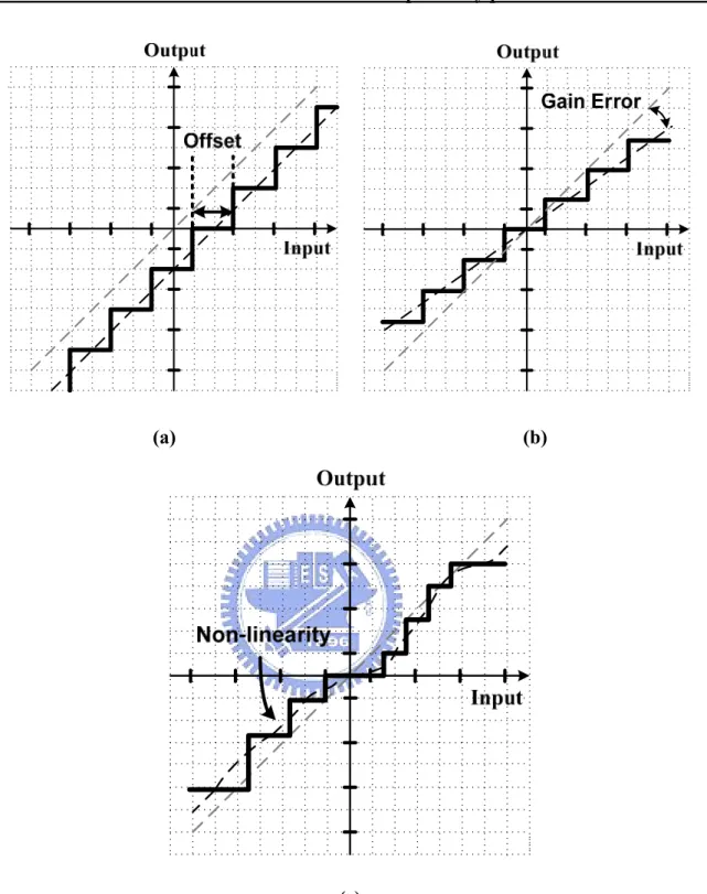
ADC has a transfer characteristic that approximates a straight line. The transfer characteristic for an ideal version of such an ADC input progresses from low to high in a series of uniform steps. However, the transfer characteristic of a practical ADC has several imperfections. Such non-idealities can be expressed in several ways as showing in Fig 2.5. In figure 2.5(a), the transfer curve all shift by a constant amount which is named offset. It may be caused by offset of operational amplifier but not affect the linearity of ADC. Figure 2.5(b) shows the practical ADC has gain error so the slope is not equal to ideal. The deviation between them comes from insufficient gain of operational amplifier and mismatch by manufacturing. In figure 2.5(c), steps are not perfectly uniform, and this deviation generally contributes to further non-idealities. Linearity error refers to the deviation of the actual threshold levels from their ideal values and is generated by distortion feature of transistor. The excessive linearity error results in missing code.
(a) (b)
(c)
Figure 2.5 Imperfections in ADC (a) Offset (b) Gain error (c) Non-linearity
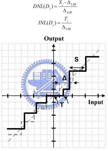
2.2.6 Differential Non-Linearity (DNL) and Integral Non-Linearity (INL)
Nonlinearity is characterized by INL and DNL admittedly. Differential nonlinearity (DNL) measures how far each of the step sizes deviates from the ideal value of the step size.
Integral nonlinearity (INL) is the difference between the actual transfer characteristic and the straight line characteristic which the ADC is intended to approximate. DNL and INL are both plotted as a function of code. DNL and INL are generally expressed in terms of least significant bit (LSB) of the input. The value of LSB has been shown by equation (2.4) previously. Figure 2.6 illustrates DNL and INL, which can be expressed as Equation (2.7) and Equation (2.8). -( ) j LSB j LSB S DNL D = Δ Δ (2.7) ( ) j j LSB T INL D = Δ (2.8)
Output
Input
T
S
Δ
Figure 2.6 DNL and INL
2.3 Review of ADC Architecture
2.3.1 Flash ADC
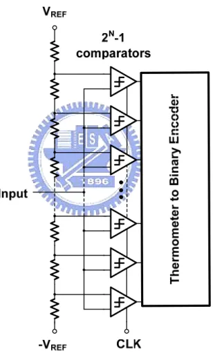
Flash ADC, which is the fastest and one of the simplest ADC architectures, is shown in Figure 2.7. It performs 2N−1 level quantization with an equal number of comparators. The
reference voltages for the comparators are generated using a resistor string, which is connected between the positive VREF and the negative -VREF reference voltage determining the full scale signal range. Together the comparator outputs form a 2N −1 bit code, where all the
bits below the comparator whose reference is the first to exceed the signal value are ones, while the bits above are all zeros. This so-called thermometer code is converted to N-bit binary code with a logic circuit, which can also contain functions for removing bit errors (bubbles).
Figure 2.7 Flash ADC architecture
The most prominent drawback of flash ADC is the fact that the number of comparators grows exponentially with the number of bits. Increasing the quantity of the comparators also increases the area of the circuit, as well as the power consumption. And the other
disadvantage is comparator offset sensitivity. At high resolutions, this required comparator offset becomes very small and are difficult to design. Thus, very high resolution flash ADCs are not practical, typical resolutions are seven bits or below.
2.3.2 Cyclic ADC
A cyclic ADC operates the same as a single pipeline stage. With the output feedback to the input, the cyclic ADC converses the data during the next clock cycle. The block diagram is illustrated in Figure 2.8. The stage conversion time from the input sample to complete digital output is the same as for a pipelined ADC. However, the throughput rate is much less than for a pipelined ADC because the entire digital word must be generated after several clock cycles passed. However, a cyclic ADC is much superior in hardware and power because of just one stage is reused repeatedly.
Figure 2.8 Cyclic ADC architecture
2.3.3 Pipelined ADC
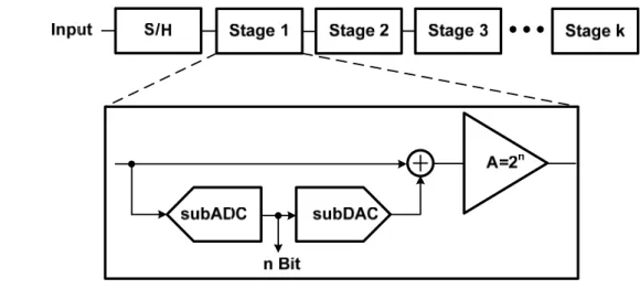
The block diagram of a typical pipelined ADC is shown in Figure 2.9. Mostly, the beginning sample and hold relaxes the timing requirements of the first stage during its sampling phase by holding the instantaneous value of the analog input. Following the S/H, it consists of a coarse subADC, coarse subDAC result, subtraction, and amplification of the remainder.
The signal is coarsely quantized by a subADC to resolve n bits. Then using a subDAC, the quantized value is subtracted from original input signal to yield the output residue. For the output signal range is the same with the input signal range for each stage, this is made by the amplifier with gain of 2n. The resulting residue signal is applied to the next stage for finer conversion on the next clock cycle. The function of the D/A, the subtraction, and the amplification of the remainder are combined into one single circuit called the multiplying DAC (MDAC).
Take 1.5bit conversion stage for example. Figure 2.11(a) shows the 1.5bit transfer curve which has three segments and is encoded as 00, 01, and 10. The input range is normally the same as output range. The conversion gain in each part is 2. The two side lines decided by subADC are 1/4VREF and -1/4VREF.
Now introduce some non-linearity affections, including of comparator offset, amplifier offset, and gain error. As illustrated in figure 2.11(b), comparator offset shifts the sight line by an offset value. Although the offset may lead output swing to over range, 1.5bit architecture has 1/4VREF tolerance of comparator offset to overcome. Figure 2.11(c) shows the amplifier offset which moves the whole conversion curve by a value. But for linearity, amplifier offset is inessential. Figure 2.11(d), gain error in subDAC, will cause the slope of transfer curve less than 2 and the output digital code will be missing.
Figure 2.10 Block diagram of radix-2 1.5b pipeline stage
(a) (b)
(c) (d)
Figure 2.11 (a) Ideal transfer curve (b) With comparator offset (c) With amplifier offset (d) With gain error
2.4 Design Issue of Pipelined ADC
2.4.1 Stage Accuracy and Speed Requirement
In the pipelined ADC, MDAC in each stage has two main specifications, speed and accuracy requirement. The speed requirement means the operation speed which is related to bandwidth of operational amplifier and feedback factor in MDAC architecture. The accuracy requirement is also affected by feedback factor but the main cause is the open-loop gain of operational amplifier. However, the constraint on each stage is different because the stage resolution decreases as the stage goes lower. Lower stage resolution means that design constraints are more relaxed. Considering the gain requirement becomes looser for later stages, several benefits are obtained if each stage is design specifically, for instance the power consumption and chip area.
General speaking, the way to implement the MDAC function is to use the switch capacitor technique. First of all, because the 1.5bit architecture is applied in this design, we just analyze this one that is shown as figure 2.12. By sampling the input signal on the capacitor and redistribution the signal charge on the capacitor, the output in hold mode is as (2.8). Note that equation ignores the time domain factor which will be discussed latter.
(
)
1 S f REF O i f S f S P f 1+C /C V V = V - D 1+C /C C +C +C C A ⎛ ⎞ ⎜⎜ ⎛ ⎞ ⎝ ⎠ ⎜ + ⎟ ⎜ ⎟ ⎝ ⎠ j⎟⎟ (2.8)Where CP is the input loading of opamp, VREF comes from subDAC, and Dj is the output of subADC. Assume CS and Cf are identical to C and the gain is larger than 1, equation (2.8) can be simplified and approximated as
2 1 1 REF REF P O i j i j P V V 2+ 2 V = V - D V - D 2+C C 2 2 A ⎛ ⎞= ⎛ ⎞⎛ − ⎜ ⎟ ⎜ ⎟⎜ ⎛ + ⎞ ⎝ ⎠ ⎝ ⎠⎝ ⎜ ⎟ ⎝ ⎠ C C A ⎞ ⎟ ⎠ (2.9)
performance, this gain error term should be less than 1LSB of the next stage resolution (z-bit) to prevent any information missing.
2 1 2 P Z C C A + < (2.10) Therefore, the specification of gain is given by
(2 )2Z P
A> +C C (2.11) Subsequently, the equation of speed requirement for the MDAC’s amplifier is derived. By assuming that the MDAC in hold mode is a single pole system and ignoring the slewing behavior, the MDAC settling time constant is
(
2 P)
u C C τ ω + = (2.12) Where ωu is unity-gain bandwidth of amplifier. Since the setting error of a single pole system is2 2 ,
T Z
e φ τ T time interval in hold mode
φ
− < − =
2 (2.13)
The constraint of unity-gain bandwidth is expressed as
2 ln 2 2 P u C Z C Tφ ω > ⎛⎜ + ⎞⎟ ⎝ ⎠ (2.14) According to equation (2.11) and (2.14), the gain and unity-gain bandwidth can be well designed to meet the constraints.
V
iC
fC
sV
OV
REFC
SC
fV
O (a) (b)2.4.2 Double Sampling
Double sampling means another duplicated path is added to let the amplifier is always in hold conversion. Output data rate is equivalently doubled without any power added. Unfortunately, several nonlinearities are also induced to decrease the efficiency, including memory effect, timing skew, and gain mismatch.
Memory effect means a fraction of the previous sample remains stored in the parasitic capacitance in the input of the amplifier due to the finite gain of the amplifier. Timing skew is caused by the distance between two adjective sampled edges is not the same as clock period. It can be found in the frequency spectrum domain. If input frequency is n Hz and sampling rate is m Hz, the timing error will be produced in the position of (m/2-n) Hz. While there is a gain mismatch between the parallel circuits, the sampling sequences they produced have different amplitudes. In the frequency domain, additional component is at multiples of half sampling rate.
Memory effect and timing skew can be suppressed by proper circuit design, which will be introduced later. Gain mismatch is avoided by symmetry layout to get better device matching.
2.4.3 Power Optimization
Error source is the random component whose dominant source is thermal noise. They are contributed by transistors in amplifier and capacitors in each stage. Assuming that thermal noise is additive Gaussian, the noise at the amplifier output appears as being superimposed on the signal. The power of the thermal noise is then described by its variance, and the variance should be much less than one LSB in order to maintain sufficiently high SNR. So, for the pipeline stage with N-bit accuracy requirement, the total input referred noise should be much
less than one LSB at N-bit level.
1
total LSB
σ < (2.20) The total input referred noise can be found by summing all the noise components from subsequent stages and is given by
2 4 4 2 2 2 2 2 1 2 3 4 1 1 1 ,where 2 2 2 total B B B j j kT C σ =σ +⎜⎛ ⎟⎞ σ +⎛⎜ ⎞⎟ σ +⎛⎜ ⎞⎟ σ + ⋅⋅⋅ σ ≅ ⎝ ⎠ ⎝ ⎠ ⎝ ⎠ (2.21)
Where B means inter stage gain which is 2 in 1.5bit architecture per stage and Cj means the thermal noise of capacitor in stage j. Notice that the dominant source of noise is from the first stage and the noise contribution from subsequent stages is reduced by the inter stage gain. Besides, equation (2.11) and (2.14) show the constraints will be relaxed down as the z parameter gets lower. Therefore, we can design stage by stage to optimize power consumption and the noise performance is still acceptable[15].
2.5 MATLAB Behavior Model
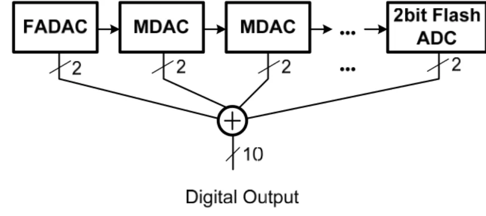
In this section, the behavioral model of a 10-bit pipelined ADC with the 1.5-bit per stage architecture is constructed by MLTLAB. The pipelined ADC consists with 9 stages is shown as figure 2.13. First stage is named FADAC[2], 2 to 8 stages use conventional MDAC and 2bit flash ADC is in final stage. Finally combine each 2bit output to produce 10bit digital code.
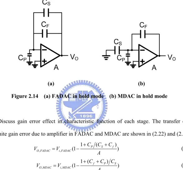
First of all is finding out all of mathematical characteristics of each block including 1st stage FADAC, MDAC, and 2bit flash ADC. The FADAC and MDAC in hold time are shown in Figure 2.14. Besides, 2bit flash ADC can be described by if-then-else syntax in coding easily.
(a) (b)
Figure 2.14 (a) FADAC in hold mode (b) MDAC in hold mode
Discuss gain error effect in characteristic function of each stage. The transfer curve with finite gain error due to amplifier in FADAC and MDAC are shown in (2.22) and (2.23).
, , 1 ( (1 + + )) = − P S f O FADAC i FADAC C C C V V A (2.22) , , 1 ( ) (1 + + ) = − f P S O MDAC i MDAC C C C V V A (2.23)
Where CP is input capacitor of Amplifier, CS and Cf are sample and hold capacitor, respectively. If the gain of amplifier is finite, VO will have gain error.
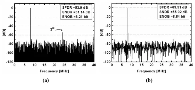
The gain of amplifier is set 48dB which is the same as the circuit level simulation result. Figure 2.15 illustrates the spectrum domain of reconstructed digital output. While calibration off, the third harmonic tone is 54dB and ENOB is 8.21bit. After calibration, SFDR increases to 70dB and it means the non-linearity is suppressed well. As the figure 2.15 shows, the calibration can effectively reduce the harmonic tone to increase the performance but notice
that the noise flow is the same no matter the calibration is on or not.
(a) (b) Figure 2.15 Simulation result of Behavior model
(a)With calibration (b)Without calibration
Then plot the curve by changing the gain value from low to high as the figure 2.16(a). With gain increasing, the resolution also increases but settles to 8.88bit finally. The least gain to achieve above 8bit is about 30dB. Figure 2.16(b) is the difference between two curves in figure 2.16(a). The improvement is over 2bit with lower gain. With gain increasing to 55dB, the improvement is down to 0bit. The trade-off range of gain between the performance and improvement is from 30dB to 50dB. In the circuit level we design is about 48dB which meets the simulation result of behavior model.
(a) (b)
C
HAPTER
3
C
IRCUIT
S
PECIFICATION
A
ND
S
IMULAION
3.1 Time-interleaved Pipelined ADC Design
3.1.1 Design Issue
In this design, in order to propose low power consumption and high speed performance, several techniques are implemented.
In the first stage, we do not use sample-and-hold circuit. All analog circuits operator under 1V supply voltage will have low power efficiency. Time-interleaved technique doubles the output throughput and calibration circuit compensates error to improve the SFDR of ADC.
Without sample-and-hold in the first stage, aperture jitter will be induced[6]. It is because the signal between subDAC catches and comparator decides may be not the same. Therefore, the larger slope of the input signal will produce the larger error. Besides, in order to minimize the total power consumption, the power supply of operational amplifier in substage is applied to 1V. So there are some challenge to do low supply voltage design including of gain and bandwidth trade-off. The proposed operational amplifier is also declared.
Third, time-interleaved technique, also named double sampling, is implemented. Output throughput can be doubled without any power consumption addition, but the timing skew effect between two sampling paths must be emphasized. Clock generator should have property of timing skew insensitive. Nevertheless, the gain of operational amplifier is not enough as usual under low supply voltage. So calibration circuit is added to boost the performance of pipelined ADC. The calibration circuit measures the error due to gain error
and compensates deviation in the digital domain finally. Ideally, by calibration circuit, the total performance will be improved. In calibration circuit, we use the successive approximation architecture (SAR). The design key points are that accuracy must be higher than pipelined ADC and offset effect need to be cancelled.
3.1.2 Architecture
1.5 bit 1.5 bit 1.5 bit 1.5 bit 1.5 bit 1.5 bit 1.5 bit 2 bit Clock Generator9-bit digital output Input
2 2 2 2 2 2 2 2
9
FADAC MDAC Flash A/D
Double Sampling 1.5 bit 2 Calibration Circuit Off-chip Calibration 7 f0 2f0 2f0 12 Phase OP Scaling ADC DAC -+ 2 DAC -2 Clk1 Clk2
Figure 3.1 Pipelined ADC and calibration circuit architecture
Figure 3.1 shows the architecture which includes two blocks. One is pipelined ADC and another is calibration circuit. Consider the low power application and the power is almost dissipated by analog circuit, we wish to design opamp under 1V operation, but full swing of clock signal is remain 1.8V to relax the switch design complexity.
Under low voltage design, the performance of pipelined ADC will be decay due to gain is insufficient. So if we can measure the deviation due to gain error and compensate the value in the digital domain, the performance can be improved ideally. Therefore, calibration circuit
produces 7-bit digital codes which are relative to the value of opamp gain error. Then, combining the digital output codes from every stage in pipelined ADC and the 7 bit codes from calibration circuit, 9bit digital codes will be produced finally.
The each block in pipelined ADC will be described subsequently. At the beginning, 12 phase clocks from clock generator drive each 1.5 bit stage to work normally. By properly trading off between speed, accuracy, and circuit complexity, we decide using 1.5bit architecture per stage. Therefore, totally 9 stages are needed. In first stage, FADAC[2] architecture is applied. Traditional MDAC is used in 2 to 8 stage and 2bit flash ADC is in final. Because just calibrating the first 6 stages, the last two stages of MDAC can be allowed to have lower accuracy and reduce the power consumption of opamp. It is the meaning of op scaling technique.
Besides, double sampling technique is applied. Adding a DAC additional path and operating the opamp not only in Clk1 but also Clk2 will equivalently double the throughput. It means that if clock speed from clock generator is f0, digital output speed will be 2f0 while double sampling technique is applied.
3.2 Each Block of Pipelined ADC
3.2.1 Operational Amplifier
(a)
M1 M2 M3 M4 M5 M6 M7 M9 M10M8 M11 M12 Vi+ VO+ VO -Vi- Vi+ Vi -VDD=1V Vb1 Vb2 (b)
Figure 3.2 (a) One stage opamp schematic (b) Proposed opamp schematic
The operational amplifier used in every stage is the most critical element of the pipelined ADC. If we want to have higher throughput of pipelined ADC, the higher unity-gain bandwidth of operational amplifier is needed, but the power consumption is also increase. With current increase, gain of operational amplifier will be decay. In addition, if we wish to increase the resolution of pipelined ADC, the operational amplifier must have higher gain. In a word, unity-gain bandwidth and gain are trade-off.
The schematic of operational amplifier used in FADAC and MDAC is shown in figure 3.2(b). Figure (a) is the simplest one stage opamp schematic. With the same current dissipation, one stage opamp will have best bandwidth performance but gain is the least. So the higher gain amplifier with split Gm stage is proposed and shown in figure (b). Comparing figure (a) and (b) under the same power consumption, architecture (b) has higher dc gain than (a) but the unity gain bandwidth are almost the same. In figure (b), additional M3-M4 pair steers the transconductance current which passes through current mirror M6-M7(M5-M10) into output node. Because of M11 current is half than M5, the output impedance will be twice than figure (a). Besides, in order to break the relation between current source M11(M12) and current mirror M6-M7(M5-M10), current injection M9-M10 is applied. In design, M11 current will be as
small as possible to get high gain and M12 current will be as large as possible to have high speed. The second pole which is at the M3(M4) drain should be well design to meet the specification of speed.
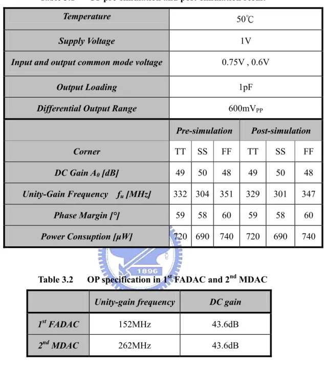
Figure 3.3(a) shows gain and phase response of amplifier simulated result and figure (b) shows opamp output range is 600mV. In table 3.1, pre-simulation and post-simulation results are shown. Opamp gain is from 48dB to 50dB in different corner cases. Now choosing total 7 bit resolution to calculate the specification about speed and accuracy. The specification of opamp dc gain is above 43.6dB in both FADAC and MDAC and unity-gain frequency constraints are shown in table 3.2. Simulation results in table 2 all satisfy the specification.
(a)
(b)
Figure 3.3 Proposed operational amplifier simulation result (a) Gain and phase response (b) Output linear range
Table 3.1 OP pre-simulation and post-simulation result
Temperature 50℃ Supply Voltage 1V
Input and output common mode voltage 0.75V , 0.6V
Output Loading 1pF
Differential Output Range 600mVPP
Pre-simulation Post-simulation Corner TT SS FF TT SS FF DC Gain A0 [dB] 49 50 48 49 50 48 Unity-Gain Frequency fu [MHz] 332 304 351 329 301 347 Phase Margin [°] 59 58 60 59 58 60 Power Consuption [μW] 720 690 740 720 690 740
Table 3.2 OP specification in 1st FADAC and 2nd MDAC
Unity-gain frequency DC gain
1st FADAC 152MHz 43.6dB
2nd MDAC 262MHz 43.6dB
3.2.2 Common Mode Feedback Cicruit (CMFB)
Common mode feedback (CMFB) specifies the output common mode voltage of differential amplifier. As the figure 3.4(a) shows, the components of CMFB are several transistor switches and four capacitors. When Clk2, the Vcmo and Vb charge to C2.Vcmo is output common mode voltage and Vb comes from bias circuit. When Clk1 becomes high, C2 connect to C1. By charge sharing, the charge in C2 will conduct to C1. As several clock period pass, the two side of C will be V and V , respectively. The V controls the current
source of amplifier to do feedback function. Consequently, output common mode voltage is set to Vcmo as expectation. In design, to avoid output voltage violation, the size of C1 is larger than C2 four to ten times.
However, because double sampling is implemented in the ADC, output node capacitive loadings are different during Clk1 and Clk2. It will induce offset between the two paths. So the CMFB circuit is modified as figure 3.4(b). In a word, figure (b) is composed of two figure (a) circuits. In each clock phase, the capacitive effects are identical.
(a)
(b)
3.2.3 Comparator
The schematic of the transconductance latched comparator[3] is shown in Figure 3.5(a). There are three advantages. One is that it can operate under low supply voltage. Second, it has no static power consumption, and third is that it is only one clock needed. When Clk is high, the two points a and b are low, and the output node, VO+ and VO-, are equally high. This is the state of reset. In this mode, M9 and M10 are ON but M14 is OFF. Because of no path to conduct any current, there have no static power consumption. As the Clk signal becomes low, comparator operates in evaluate state. The two input pairs M5-M8 can be to consider as two resistances and the values are dependent on differential input and reference voltages. According to the resistances of two points a and b are low or high, it will introduce a small voltage difference between them. Then, M3 or M4 becomes ON, the set of cross couple pairs, M1-M4, will separate the difference to full scale. Finally, VO+ and VO- are generated and the value is written as
{
}
O V = 1 (3.1) 0 i R i R if V V if V V > < ef efIn the evaluate state, when one of the two points, a and b, is higher than threshold voltage of inverter, M9 or M10 will be turned off. It can be find no DC current path and no DC power consumption. Figure 3.5 shows the comparator simulated result. Assume VREF is zero, the function between Vi and VO is correct.
(a)
(b)
Figure 3.5 (a) Comparator schematic (b) Comparator simulated result
Due to mismatch and layout asymmetry, comparator will have offset voltage. However, comparator offset is allowed in 1.5bit per stage pipelined ADC. In this design, the tolerance is about 75mV. To emulate mismatches, randomly change the Vt0, channel width (W), and channel length (L) variations. Their standard deviations are
Vt t A 1 σ(ΔV )= 2 WL A σ(W) 1= W 2 WL β
Table 3.3 Mismatch parameter
AVtn 3.73mV×μm Aβn 0.3635%×μm
AVtp 3.26mV×μm Aβp 0.4432%×μm
From 500 time Monte Carlo simulations, the distribution of offset voltage is plotted in figure 3.6(a). By estimating as Gaussian distribution, the standard variation (σ) is 11mV. This value satisfies the constraint of comparator offset. Figure 3.6(b) shows the relation between the times of Monte Carlo simulation and offset value. As times number increase, the curve will settle to 11mV.
(a) (b) Figure 3.6 (a) 500 times Monte Carlo simulation
(b) Times of Monte Carlo simulation and offset value relation
3.2.4 The 1.5 bit flash ADC
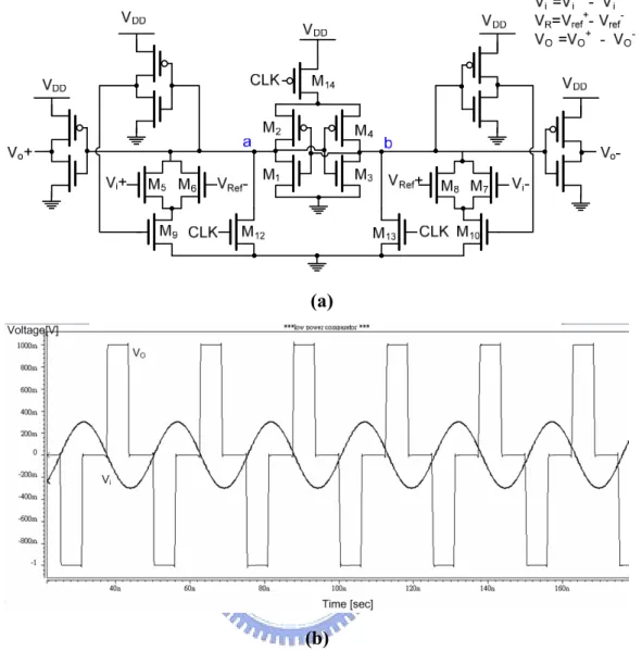
Figure 3.7 shows the 1.5bit flash ADC schematic. Signal Vi is the input and output is digital code “D1D2”. They consist of two comparators, three level converters, and several logic gates. The last two elements are called encoder. The circuit is to convert input signal to digital level expression, as the table 3.4 shown.
Table 3.4 Input level expression Condition D1 D2 D3 (1V swing) S1 S2 S3 (1.8V swing) Vi>(1/4)VRef 1 0 0 1 0 0 -(1/4)VRef <Vi<(1/4)VRef 0 1 0 0 1 0 Vi<-(1/4)VRef 0 0 1 0 0 1
Instinctively, three NOR gates is applied to produce digital codes. Besides, it also has to switch the transistors in FADAC and MDAC circuit. Because the operation must be lager than phase of Clk2 and supply voltage levels are different, three NAND gates and three level converters are needed.
Figure 3.7 1.5bit flash ADC schematic
3.2.5 Flip-around DAC (FADAC)
Figure 3.8 is FADAC architecture which has been employed in an 125MHz 10bit pipeline ADC[2]. There are two features in this circuit. One is that feedback factor is almost equal to one in hold mode, so having good performance in speed and accuracy. Another is
because of gain is half one in hold mode, input range need to be amplified four times than output. Clock waveform is shown as figure (c). During Clk1, figure (a), input is sampled in CS1 and another three references are sampled in CS1, CS2, and CS3. The three references is +2VREF, 0, and -2VREF, respectively. Then, comparators estimate the input level when Clk1 becomes high to low. When Clk2 is high, capacitor is switched adequately by decoder and flipped-around with CS1 to the output node. By charge sharing and parallel connection, the input transfer function is represented as (4.2).Assume CS1=CS2=CS3=CS4,
i i i
1
V = V +bV
2 Ref (3.2)
Where bi is +1 if digital code is “00”; bi is 0 if digital code is “01”; bi is -1 if digital code is “10”.
Figure (d) is the INL plot of FADAC. The transverse axle means input value which is from -1.2V to +1.2V. The INL, ideal output value minus real output then referred to input, is defined as (4.3), i i Ref O 1 [( V +bV )-V ] 2 INL = 2 (3.3)
(a) (b)
(c) (d)
Figure 3.8 FADAC schematic
(a) During Clk1 (b) During Clk2 (c) Clock waveform (d)INL plot
Without sample-and-hold amplifier in the first stage, the aperture jitter will be induced[6]. In figure 3.9(a), while data sampled in CS1 differ from comparator estimate, it will cause error that can not be compensated. Therefore, the input stage in FADAC is shown in figure 3.8(a). Adding CC1 and CC2 sample paths to match CS1 path to make sure data in CS1, CC2, and CC1 are identical during Clk1 phase. Figure (b) shows the clock waveform, clkb and Clkc are applied additionally.
(a) (b)
Figure 3.9 (a) FADAC input sampling circuit (b) Clock waveform
3.2.6 Bootstrapped Switch
Bootstrapped switch supports constant conductive impedance and is used to cancel the input dependent non-linearity. Figure 3.10 shows the schematic. Clkb is complementary to Clk. when Clk is low, the voltage in right side of capacitor C1 is VDD, and left side is gnd, so C1 is store the voltage drop of VDD. When Clk becomes high, the right side of C1 connects to M9 gate and left side connects to Vi. It means the gate drive between M9 gate and source will hold out VDD. Therefore, M9 has a good performance in linearity. The M8 transistor is added to reduce the maximum VDS of M5.
Figure 3.11(a) is the circuit to simulate the linearity of bootstrapped switch. Figure 3.11(c) shows the SFDR of bootstrapped switch while input frequency is 40MHz and switch clock rate is 80MS/s. Then change input frequency to plot the SFDR curve of output FFT. The simulated result is shown in figure 3.11(b). From low input frequency to high, the SFDR are all above 78dB. Figure 3.11(d) is the time domain simulation result where the VO and Vi have constant voltage gap 1.8V.
C
1C
2Bootsw
V
iM
1V
oV
G (a) (b) (c) (d)Figure 3.11 (a) Circuit to simulate SFDR of bootstrapped switch (b) Dynamic simulation with different input frequency
(c) SFDR is 78dB when input frequency is 40MS/s and switch clock rate is 80MS/s (d) Time domain simulation
3.2.7 Multiply DAC (MDAC)
Figure 3.12 is conventional MDAC architecture. Clock waveform is shown as figure (c). During Clk1, figure (a), input is sampled in CF and CS. Then, comparators estimate the input level when Clk1 becomes high to low. When Clk2 is high, CF flipped-around to output and encoder switches the adequate reference voltage to CS to do the operation of subtraction and multiplication. The three references is +VREF, 0, and -VREF, respectively. By charge conservation rule, the input transfer function is represented as (3.4).Assume CF=CS,
Ref
i i i
V = 2V +bV (3.4)
Where bi is +1 if digital code is “00”; bi is 0 if digital code is “01”; bi is -1 if digital code is “10”.
Figure (d) is the INL plot of MDAC. The transverse axle means input value which is from -0.3V to +0.3V. The INL, ideal output value minus real output then referred to input, is defined as (3.5),
i i Ref O
[(2V +bV )-V ] INL =
2 (3.5)
VO Encoder +(1/4)VRef -(1/4)VRef 0 -VRef +VRef
Selects 1 switch out of 3 Cf +Vi Cs (a) (b) (c) (d) Figure 3.12 MDAC schematic
(a) During Clk1 (b) During Clk2 (c) Clock waveform (d) INL plot
3.2.8 Double Sampling
In order to double the output throughput, the technique of double sampling is realized. Easily, add another path to convert the input signal. Figure 3.12(a) and (b) mean the MDAC circuit during Clk1 and Clk2. When Clk1 is high, Cf1 and CS1 are applied to be sampled capacitors. Besides, Cf2 and Cs2 are flipped-around to be hold capacitors. During Clk2, Cf1 and CS1 are replaced to Cf2 and CS2. Cf2 and CS2 become hold capacitors. By applying the technique, the opamp is always in used but has no power dissipated additionally. But, memory effect is induced as well. Due to the finite gain of the opamp a fraction of the previous sample
remains stored in the parasitic capacitance in the input of the opamp. Therefore, add clock Clkrst between Clk1 and Clk2 to cancel the memory effect. As the figure 4.12(c) shows, the opamp resets its input and output to common mode voltage during Clkrst. And figure (c) is the clock waveform.
(a) (b)
(c) (d)
Figure 3.13 Double sampling
(a )During Clk1 (b) During Clk2 (c) During Clkrst (d) Clock waveform
3.2.9 Final 2bit flash ADC
Figure 3.14(a), (b) shows the truth table and implemented schematic. Figure (c) is the simulation result. The two threshold voltages is ±(1/2)VREF and 2bit digital output is ”D1D0”.
(a) (b)
(c)
Figure 3.14 2bit flash ADC
(a) True table (b) Gate level implement (c) Simulation waveform
3.2.10 Clock Generator
Figure 3.15 shows the clock generator schematic and waveform diagram. Because of the use of double sampling technique, we need to be aware of the clock skew effect. As the mark 1 show, creating a Gating signal to make sure the space between Clkf1 and Clkf2 falling edges can reduce clock skew. Mark 2 indicates Clkd1 falling production. Besides, we should let the point a and b have the same delay, so a transmission gate is added. It is shown as mark 3. By tuning the size of transmission gate, we can get the best situation which has least clock skew effect. Figure (c) shows the simulation result.
(a) (b)
(c)
Figure 3.15 (a) clock generatior schematic (a) waveform diagram (c) simulation resolutoin
3.2.11 Timing Diagram
The important role in pipelined ADC is timing diagram. Figure 3.16 shows the timing diagram which ensures the ADC function correctly in timing sequence. Q1 and Q2 are alternate each other and represent the two channels under double sampling. Mark 1 shows FADAC samples data and comparator evaluates at this time. Mark 2 means encoder decides to do right subtraction and FADAC transit to hold mode. At the same time, MDAC in next stage
is in sample mode. Then, Mark 3 is the time at the end of MDAC hold state. Mark 4, the signal has already settled accurately and MDAC transit sample state to hold mode.
Besides, Clkrst introduced in 3.2.8 Double Sampling is between two adjacent states to cancel the memory effect.
C
HAPTER
4
C
ALIBRATION
C
IRCUIT
4.1 Calibration Conception
(a) (b) (c)Figure 4.1 (a) Ideal and real transfer curves (b) FADAC in hold mode (c) MDAC in hold mode
Figure 4.1 shows the radix-2 1.5bit transfer curve in MDAC circuit. The transverse axle means input value and longitudinal axle is output value. Black line is ideal curve and each
slope in the three segments is 2. Red line is less than 2 due to opamp gain error. Define slope in black line is Gn, slope in red line is Gn’. Figure 4.1(b) is FADAC circuit in hold mode and (c) is MDAC circuit in hold mode. By hand calculation, assume C=CS=CF, the slope can be written
(
)
' ' 1 2 1 1 2 1 1 2 2 1 1 1 2 P n G n n P P n n n P C G C G in FADAC G G C A A C C G C G in MDAC G G C A A C ⎛ + ⎞ ⎜ ⎟ n n G Δ ⎛ ⎞ = = ⎜ − ⎟= ⎜ ⎟ ⎛ ⎞ ⎜ ⎟ ⎝ ⎠ + +⎜ ⎟ ⎜⎝ ⎟⎠ ⎝ ⎠ ⎛ + ⎞ ⎜ ⎟ = = ⎜ − ⎟= ⎛ ⎞ ⎜ ⎟ +⎜ + ⎟ ⎜⎝ ⎟⎠ ⎝ ⎠ − − Δ (4.1) Where 2 P G C C A +Δ = is gain error in MDAC. By (4.1), error in FADAC is half than which in
MDAC due to the feedback factor in MDAC is almost twice than which in FADAC.
Then, define G=G1=G2, and assume the first stage is FADAC and others are MDACs, from 10bit analog to digital conversion equation
(
)
(
)
3 9 2 1 ' ' ' ' ' ' 1 1 2 1 2 8 7 3 9 2 1 2 8 ... ... 1 1 1 ... 1 1 2 2 2 da da da da da da da da G G G G G A A A A A G G G G G G A A A A G G G = + + + + Δ Δ Δ ⎛ ⎞ ⎛ ⎞ ⎛ ⎞ = + ⎜ + ⎟+ ⎜ + ⎟ + Δ + + ⎜ + ⎟ + Δ ⎝ ⎠ ⎝ ⎠ ⎝ ⎠ (4.2)where A is the input signal, Anda is digital code from n-th subADC output, G is ideal conversion gain and G’ is real conversion gain.
The value of ΔA is what the calibration circuit need to measure. By (4.2) constructed, the gain error can be compensated ideally. So the performance of pipelined ADC should be improved.
4.1.1 Nonlinearity of gain
In the above discussion, the gain is assumed as a constant value. Accordingly, the transfer curve of each section is approximated to a straight line. In practical, the output impedance is dependant on the output value, so the gain value also varies with the output. As
the figure 4.2 shows, the slope of G’ due to gain deviation is various with a small range. Define the gain deviation due to gain nonlinearity
0 0 -A A A A Δ = (4.3)
Where A0 is the gain without gain deviation and A is the gain with gain deviation. By the intuition, set parameter k is improvement of calibration circuit. We can get
2
k AΔ <
(4.4) On the other hand, the nonlinearity of gain is the dominant influence in the efficiency of calibration. Figure 4.3 shows the simulated nonlinearity of opamp which is the same as figure 3.2(b) shows. With the corner simulation, the gain deviation is about 25%. By the equation of (4.4), the improvement can be near 2 bit.Figure 4.2 Slope deviation due to gain deviation
4.2 Calibration Circuit
Figure 4.4 shows the calibration circuit which is applied to measure the gain error. The components are two opamps, one comparator, and an accumulator. One of the opamps is the same as which in first several stages and the other has higher gain to have higher resolution. In Clka, Vi samples to CF and CH. when Clkb becomes high, due to the gain error VO is a slightly smaller than Vi. Define the difference is symbol of Δ. Furthermore, Vout is much close to Vi because AC gain is high. Then, Clk1 and Clk2 start to become high alternately. So Vout decreases one Δ as one clock period passes. As the figure (b) shows, while Vout becomes less than zero, comparator lets the accumulator stop counting. At this time, digital code output is produced and shown as (4.4).
(a) (b)
Figure 4.4 (a) Calibration circuit (b) Clock and output waveform
P PC C P C P C P G C - C A A A Digital Code = n = ( )(1- + ) if A << A C A C A 2+ C (2+ C)C A 1 ( ) = C 2+ C ≅ Δ (4.5)
From (4.5), there are a simple relation between Digital Code and gain error. Then combine
3 9 2 1 ' ' ' ' ' ' 1 1 2 1 2 8 7 3 9 2 1 2 8 ... ... 1 1 1 1 1 1 1 ... 1 1 2 2 2 da da da da da da da da A A A A A G G G G G G A A A A G n G n n G n n = + + + + ⎛ ⎞ ⎛ ⎞⎛ ⎞ ⎛ ⎞⎛ = + ⎜ + ⎟+ ⎜ + ⎟⎜ + ⎟+ + ⎜ + ⎟⎜ + ⎝ ⎠ ⎝ ⎠⎝ ⎠ ⎝ ⎠⎝ 1⎞⎟ ⎠ (4.6)
Where n is the calibration circuit output, G is ideal conversion gain, and Anda is digital code from n-th subADC output. Equation (4.6) means the compensated operation in off-line calibration and illustration is shown in figure 4.5. The division and add operations are needed.
⎛ ⎞ ⎜ ⎟ ⎝ ⎠ 1 1 + 2n ⎛ ⎞⎛ ⎞ ⎜ ⎟⎜ ⎟ ⎝ ⎠⎝ ⎠ 1 1 1 + 1 + 2n n ⎛ ⎞⎛ ⎞ ⎜ ⎟⎜ ⎟ ⎝ ⎠⎝ ⎠ 7 1 1 1 + 1 + 2n n
Figure 4.5 Illustration of off-line calibration operation
4.3 Operation Amplifier in Calibration Circuit
In calibration circuit, a high gain opamp is needed but the unity-gain frequency and output swing is not required strictly. As the figure 4.6(a) shows, folded-cascoded opamp is applied. The output swing just needs 150mV, so the VDD is allowed to be 1V. The wide swing cascode bias circuit is shown in figure 4.6(b). The common mode feedback circuit (CMFB) is used as figure 3.4(a). The simulation result is shown in table 4.1. The dc gain is 64dB and power consumption is 220μW.
(a) (b) Figure 4.6 (a) Amplifier in calibration circuit (b) Bias circuit
Table 4.1 Amplifier in calibration circuit simulated result
Temperature 50℃
Supply Voltage 1V
Input and output common mode voltage 0.75V , 0.5V
Output Loading 0.2pF
Differential Output Range 300mVPP
Corner TT SS FF DC Gain A0 [dB] 64.4 63.3 64.3 Unity-Gain Frequency fu [MHz] 100 94.5 103 Phase Margin [º] 58 59 57 Power Consuption [μW] 220 210 225