Metal nanocrystals as charge storage nodes
for nonvolatile memory devices
P.H. Yeh
a, L.J. Chen
a,∗, P.T. Liu
b,
D.Y. Wang
c, T.C. Chang
d,eaDepartment of Materials Science and Engineering, National Tsing Hua University, Hsinchu, Taiwan, ROC bDepartment of Photonics and Display Institute, National Chiao Tung University, Hsinchu, Taiwan, ROC cElectronics Research and Service Organization, Industrial Technology, Research Institute, Hsinchu, Taiwan, ROC dDepartment of Physics and Institute of Electro-Optical Engineering, National Sun Yat-Sen University, Kaohsiung, Taiwan, ROC
eCenter for Nanoscience & Nanotechnology, National Sun Yat-Sen University, Kaohsiung, Taiwan, ROC Received 27 May 2006; received in revised form 20 July 2006; accepted 2 September 2006
Available online 10 October 2006
Abstract
The memory effects of the metal nanocrystals were found to be more pronounced than those of the semiconductor nanocrystals. Various metal nanocrystals as charge storage nodes are reviewed. The memory effects have strong relationship with the work function, and the work function can be modulated by changing the metal species. By tunneling dielectrics engineering, the optimum IG Write/Erase/IG Retentionratio can be obtained.
© 2006 Elsevier Ltd. All rights reserved.
PACS: 68.37.Lp; 73.63.Kv; 73.22.−f; 73.21.La
Keywords: Ni nanocrystals; NiSi2nanocrystals; CoSi2nanocrystals; Metal nanocrystals; Nonvolatile memory
1. Introduction
The flash memories have evolved from single device com-ponents to megabit nonvolatile memory (NVM) arrays [1]. Flash memories are easily scalable replacements for erasable programmable read only memory (EPROMs) and electrically erasable programmable read only memory (EEPROMs). Unlike EPROMs and EEPROMs, flash memory cells provide single-cell electrical program and fast simultaneous block electrical erase. Thus, a small cell size is combined with a fast in-system erase capability.
These low-power and powerful flash systems are ideal for a myriad of portable applications such as cellular phones, digi-tal cameras, digidigi-tal voice recorders, notebook computer, MP3 walkman, personal data assistants to compact smart cards, USB flash personal disc, etc. These products have been widely used and play important roles in the consumer market. They may eventually replace the ubiquitous magnetic memory media and
∗Corresponding author.
E-mail address:[email protected](L.J. Chen).
random access memories (RAMs) in many compact electronic applications[2].
The effective flash technology compatible with the standard complementary metal-oxide-semiconductor (CMOS) device process flow presents some challenges. The bigger one is the inter-related scaling requirements for voltage and gate oxide for embedded flash devices. The aggressive scaling of gate dielec-tric to control deleterious short-channel effects in logic devices is intrinsically incompatible with the need to preserve minimum dielectric thickness in flash devices to maintain oxide reliability and data-retention after many write/erase cycles[3].
Furthermore, the program and erase voltages of flash devices are typically above 10 V. This is far too large for the one-volt-operation of logic CMOS devices. Erratic failure bits and increase in leakage-current when a device is stressed under high bias conditions compromise memory performance. As a result, research is moving along the following paths for embedded flash devices:
(1) scaling down the cell size of device memory; (2) lowering voltage operation;
0013-4686/$ – see front matter © 2006 Elsevier Ltd. All rights reserved. doi:10.1016/j.electacta.2006.09.006
(3) increasing the density of state per memory cell by using a multi-level cell.
To sustain the continuous scaling, conventional flash devices may have to undergo revolutionary changes. Novel device con-cepts with new physical operation principles are needed[4–8].
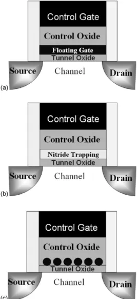
A memory cell is a system element that contains 1-bit of information. The standard commercial flash device is similar to the Intel EPROM Tunnel Oxide (ETOX) structure, as shown inFig. 1(a). The basic device is a MOS-field-effect-transistor (MOSFET) with a modified gate stack structure that has a control gate (CG) and a floating gate (FG) embedded in a dielectric material such as SiO2[9].
Thus, flash memory cell scaling below the 0.1m fea-ture size will be difficult, if channel-hot-electron (CHE) and Fowler–Nordheim (FN) injection processes are involved in the program and erase operations [3]. To circumvent these limi-tations, new device concepts that are more robust to leakages through oxide defects are being considered. Among the recent proposals are the silicon/oxide/nitride/oxide/silicon (SONOS),
Fig. 1. The device structures of: (a) conventional nonvolatile flash, (b) SONOS stored unit nonvolatile flash, and (c) nano-dots stored unit nonvolatile flash.
the nitride read-only memory (NROM) and the nanocrystals charge-storage nodes memories. The SONOS structure is shown inFig. 1(b).
These technologies replace the extended floating gate struc-ture with a great number of charge-storage nodes in the dielec-tric. Unlike the extended floating gate, stored charges in isolated nodes cannot easily redistribute amongst themselves. If the stor-age node density is much higher than the defect density in the isolation dielectric, only a relatively small number of nodes will be drained by defects. This effectively prevents the leakage of all the stored charge out of the floating gate.
2. Nanocrystals structure
Beside the SONOS structure, Tiwari et al. first proposed flash memory with a floating gate made out of silicon nanocrystals [8]. The nanocrystals are extremely small clusters of Si atoms ranging from 5 to 10 nm in diameter. As illustrated inFig. 1(c), the nanocrystals embedded between the tunneling and control-ling dielectric. By limiting nanocrystals deposition to just one layer and adjusting the thickness of the top controlling dielectric, charge leakages to the control gate from the nanocrystals can be effectively prevented. Also, compared to the atomic-size nitride traps, electron or hole energy states are energetically deeper in the nanocrystal wells. Conceptually, the increased confinement and the reduction in leakages imply that tunneling oxide can be more aggressively scaled down. With a thin tunnel oxide, direct quantum-mechanical tunneling can be exploited as a trans-port mechanism for programming and erasing the charges in the nodes.
Memory-cell structure using nanocrystals as the charge stor-age media have received much attention as the promising can-didates to replace conventional dynamic random array memory or flash memories for future high speed and low power con-sumer memory devices [8,10,11]. Most studies have focused on the fabrication on Si and Ge nanocrystals in metal-oxide-semiconductor (MOS) structure [12–20]. In addition, atomic-force-microscopy (AFM) was utilized to inject charges in the nanocrystals[21–23]. The use of a floating gate composed of distributed nanocrystals reduces the problems of charge loss encountered in conventional floating-gate electrically erasable programmable read-only memory devices. It allows thinner tunnel oxide and, thereby, smaller operating voltages, bet-ter endurance and retention, and fasbet-ter program/erase speed [13–15].
In optimizing such devices, the ideal goal is to achieve the fast write/erase of DRAM and the long retention time of flash memories simultaneously. For this purpose, we need to create an asymmetry in charge transport through the gate dielectric to maximize the IG Write/Erase/IG Retentionratio. For dielectrics engi-neering, by replacing the rectangular barrier with a parabolic or triangular barrier, the barrier height can be modulated by the electric field in the tunnel oxide[24]. In practice, the parabolic or triangular barrier can be simulated by stacking multiple layers of dielectrics.
Another approach is to use double-stacked storage nodes, preferably self-aligned with smaller dots at the lower stack. In
Fig. 2. Energy band diagram for embedded metal nanocrystals between control oxide and tunnel oxide.
such devices, fast write/erase can still be achieved, if sufficiently thin tunnel oxides are used below and between the two stacks. However, the retention time can be significantly improved due to the Coulomb blockade effect at the lower stack, which prevents electrons in the top stack storage nodes from tunneling back into the substrate[25].
The third approach, which is the focus of this paper, is to engineer the depth of the potential well (deff) at the storage nodes, thus creating an asymmetrical barrier between the substrate and the storage nodes, i.e., a small barrier for writing and a large barrier for retention. This can be achieved if the storage nodes are made of metal nanocrystals. The energy band diagram for embedded metal nanocrystals between control oxide and tunnel oxide is shown inFig. 2.
In this paper, we will discuss unique features of metal nanocrystal memories in comparison with their semiconductor counterparts. The metal nanocrystal memory possesses several advantages, such as stronger coupling with the conduction chan-nel, a wide range of available work functions, higher density of states around the Fermi level and smaller energy perturbation due to carrier confinement[26].
3. Work function engineering
The memory effects of the Ag, Au, Pt, W, Co, Ni, NiSi2, Ni1− xFex, TiN and Al metal nanocrystals were investigated
[26–43]. Devices with Au, Ag and Pt nanocrystals working in the F–N tunneling regime have been investigated and compared with Si nanocrystals memory devices. The memory effect will be seen when the effective potential well depth (deff) is higher. As a result, the memory effects of the Pt and Au are better than the Ag[26–29]. The work functions of various metallic materials are listed inTable 1.
For the industrial applications, the Pt and Au are precious metals that would increase the fabrication cost. Therefore, metal-lic materials with high work function, but not the precious metals, are more desirable. There are a number of reports on high work function materials with significant memory effects [30–43]. For example, good memory effects were found for
Table 1
Work functions of various metallic materials
Element Work function,Φ (eV)
Au 5.10± 0.1 Ag 4.33± 0.15 Pt 5.32± 0.1 W 4.55± 0.1 Ni 4.96± 0.1 NiSi2 4.71± 0.1 CoSi2 4.70± 0.1 Al 4.24± 0.1 TiN 2.92± 0.1
devices with the W nanocrystals and the work function of W is 4.55 eV[30,31].
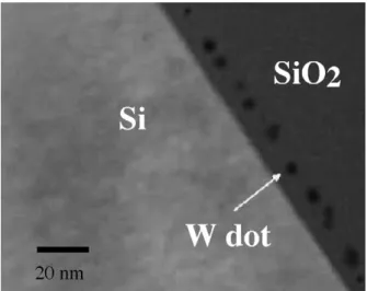
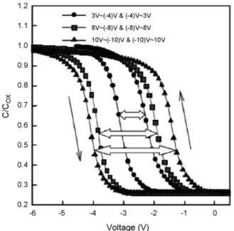
The W-rich tungsten silicide layer, W5Si3, was physically sputtered onto the tunnel oxide. The W5Si3layer was capped by an amorphous-Si layer deposited also by sputtering. The stacked structure was, afterwards, dry oxidized at 900◦C to form a layer with control oxide on the top and W nanocrystals precipitated and embedded between tunnel oxide and control oxide.Fig. 3represents a typical bright-field, cross-section TEM image. Spherical and well-separated W nanocrystals embed-ded in the SiO2 layer are clearly observed. Fig. 4shows the capacitance–voltage (C–V) hysteresis after bidirectional sweeps, which implies the electron charging and discharging effects of W nanocrystals embedded in SiO2. InFig. 4, with the voltage swept from 3 to (−4) V and back to 3 V, a significant thresh-old voltage shift of 0.95 V is observed. As the swept voltage is increased to 8 V or 10 V, a more pronounced C–V shift is observed. It is worth noting that the hysteresis is counterclock-wise which is due to substrate injection from the electrons of the deep inversion layer and holes of the deep accumulation layer of Si substrate[44].
Ni, NiSi2 and CoSi2 nanocrystals embedded in the SiO2 exhibiting memory effects have been formed; the cross-section TEM images and C–V hysteresis are shown inFigs. 5–7, respec-tively. The Ni nanocrystals embedded in the SiO2layer has been formed by rapid thermal annealing of a SiO2/Ni/SiO2structure at
Fig. 4. The capacitance–voltage (C–V) hysteresis after bidirectional sweeps, which implies the electron charging and discharging effects of W nanocrystals embedded in SiO2.
Fig. 5. The C–V hysteresis of Ni nanocrystals embedded in SiO2. Inset is the cross-section TEM image. Well-separated and spherical Ni nanocrystals are seen.
Fig. 6. The C–V hysteresis of NiSi2nanocrystals embedded in SiO2. Inset is the cross-section TEM image. Well-separated and spherical NiSi2nanocrystals are seen.
Fig. 7. The C–V hysteresis of CoSi2nanocrystals embedded in SiO2. Inset is the cross-section TEM image. Well-separated and spherical CoSi2nanocrystals are seen.
400◦C. The NiSi2and CoSi2nanocrystals have been formed by thermal oxidation of an amorphous-Si/Ni/SiO2and amorphous-Si/Co/SiO2structures, respectively. The stacked structure was, afterwards, dry oxidized at 900◦C to form a layer with control oxide on the top and NiSi2or CoSi2nanocrystals precipitated and embedded between tunnel oxide and control oxide. The insets ofFigs. 5–7are the cross-section TEM images showing the well-separated and spherical Ni, NiSi2and CoSi2 nanocrys-tals, accordingly. The mean sizes of the Ni, NiSi2 and CoSi2 nanocrystals are 3.7, 7.6 and 4.4 nm, respectively. The signif-icant threshold voltage shift of 1 and 1.1 V are seen for NiSi2 and CoSi2nanocrystals, correspondingly, as the charge storage nodes at low voltage operation, respectively.
Other nanocrystals as the charge storage nodes, like TiN and Al, with memory effects have also been studied [32–34]. The memory windows are sufficient to be defined as “1” and “0” by a typical sensing amplifier for a memory device. Using the metal nanocrystals to be the charge storage nodes, vari-ous dielectrics were used for the tunnel dielectric to maximize the IG Write/Erase/IG Retentionratio. The influence of the tunneling dielectric to the memory effect is also addressed.
4. Dielectric engineering
The fabrications of the metal nanocrystals using other tun-neling and capping dielectrics have attracted a great deal of interest. Nonvolatile memory with Ni nanocrystals embedded in HfO2has been investigated. The initial Ni layer thickness and annealing temperature were found to influence the Ni nanocrys-tal formation[35–37]. The size and density of the nanocrystals were found to increase and decrease with the annealing temper-ature, respectively.
NiSi2 nanocrystals embedded in the SiO2 layer exhibiting memory effect has been formed[38,39]. The NiSi2 nanocrys-tals using the SiO2and HfO2for the tunneling dielectrics were also fabricated. Two sets of samples (samples A and B) were prepared. Samples A and B consist of 3-nm-thick SiO2and 2-nm-thick HfO2/1-2-nm-thick SiO2 as the tunneling dielectrics, respectively. The detailed conditions for the preparation of
Table 2
Detailed conditions for the preparation of samples A and B Samples A B SiO2(nm) 1 3 HfO2(nm) 2 – Ni (nm) 1.5 1.5 Si (nm) 3.5 3.5 Anneal (◦C) 600 600 HfO2(nm) 18 18
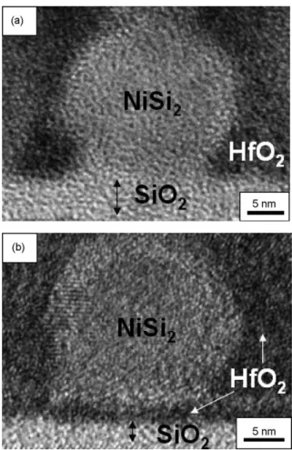
the samples A and B are listed in Table 2. The cross-section TEM images of the NiSi2using the SiO2and HfO2tunneling dielectrics are shown inFig. 8. One nanometer-thick SiO2in the samples B was used to improve the flat interface between the Si substrate and the tunneling HfO2. The physical thickness of samples A and B are all 3 nm, but the effective oxide thickness (EOT) of the samples B is 1.5 nm, which is half of that in sam-ples A. So the memory effect will be increased, when using the HfO2to replace the SiO2for the tunneling dielectric at the same programming voltage, as shown inFig. 9. The memory windows of the NiSi2using SiO2and HfO2tunneling dielectrics are 1.04 and 1.38 V, respectively. The memory window of the samples with HfO2tunnel dielectric is larger than the samples with SiO2
Fig. 8. (a and b) The NiSi2nanocrystals with SiO2and HfO2tunnel dielectrics, respectively.
Fig. 9. The C–V hysteresis of the NiSi2 using SiO2 and HfO2 tunneling dielectrics. The memory windows of the NiSi2using SiO2 and HfO2 tunnel-ing dielectrics are 1.04 and 1.38 V, respectively.
owing to the smaller voltage drop for HfO2tunnel dielectric with the same physical thickness.Fig. 10shows the retention charac-teristics for the samples A and B. The retention characcharac-teristics were rather poor for the samples B. It is ascribed to the EOT (1.5 nm) being too thin so that the electrons can tunnel back eas-ily. The physical thickness of HfO2tunnel dielectric is enough for the small operation voltage, but not adequate for the reten-tion requirement. The tunneling probability of electron is related to the thickness and the barrier of the tunnel dielectric.Fig. 11 shows the band diagrams of NiSi2 nanocrystals with SiO2 or HfO2tunnel dielectrics after programming. When the device is written or programmed, the electrons directly tunnel from the Si substrate through the tunnel dielectric, and are trapped in the NiSi2nanocrystals. Without applied voltage, the band diagrams are shown asFig. 11(a and b) for SiO2and HfO2, respectively. At this stage, the electrons may tunnel back to Si substrate. The tunnel probability of electrons is strongly related to the thickness and barrier of the tunnel dielectrics without operation voltage. In the present investigation, the samples using HfO2appear to be inferior to the SiO2tunnel dielectric in the retention characteris-tics. But if the optimum thickness of the HfO2can be found, it is
Fig. 10. The retention characteristics for the samples A and B. The retention characteristic was rather poor for the sample B. It is ascribed to the EOT (1.5 nm) is too thin so that the electrons can be tunneled back easily.
Fig. 11. The band diagrams of NiSi2nanocrystals with SiO2or HfO2 tunnel dielectrics after programming.
possible that more favorable maximum IG Write/Erase/IG Retention ratio can be obtained.
There are other dielectrics used as the tunneling dielectrics. As an example, self-assembled Ni1− xFexnanoparticles
embed-ded in a polyimide (PI) matrix were formed by curing Ni1− xFex
thin films with polyimide precursor layers[40]. The Ni1− xFex
nanocrystals were created inside the PI layer. The process can be conducted at relatively low temperature with the highest tem-perature being 400◦C.
For the various metal nanocrystals as the charge storage nodes described, the memory effects of the various metal nanocrystals are summarized inTable 3.
Table 3
Memory effects of various metal nanocrystals
Element Tunnel dielectric Vth, C–V (V) Sweep voltage (V)
Au SiO2 2.3 2 to−4 Ag SiO2 2.1 2 to−4 Pt SiO2 3.8 2 to−4 W SiO2 0.95 3 to−4 Ni SiO2 0.52 6 to−6 HfO2 0.75 2 to−2 NiSi2 SiO2 1.04 3 to−3 HfO2 1.38 3 to−3 CoSi2 SiO2 1.1 3 to−3 Al AlN 1 5 to−5 Ni1− xFex PI 2 11 to−6 TiN Al2O3 2.9 NA
5. Room temperature deposition
In addition to the metal nanocrystals fabricated by ther-mal annealing, there are other fabrication processes to form the metal nanocrystals. The Langmuir–Blodgett technique is a room-temperature deposition process that may be used to deposit monolayer and multilayer films of organic materi-als. Furthermore, this method permits the manipulation of organic molecules on the nanometer scale, thereby allowing intriguing superlattice architectures to be assembled [45]. The Langmuir–Blodgett deposition of organically passivated Au nanoparticles is reported [41]. A monolayer of these particles has been incorporated into a MIS structure.
6. Four bits per cell
Scaling down the memory device is to increase the density of the memory cell for NVM, but there is scaling limitation to all NVM technologies. Instead of scaling down NVM, one impor-tant new innovation is multi-bits per cell. Based on the 2-bits per cell metal nanocrystal memories[27], a novel quad source/drain device capable of 4-bits per cell data storage is demonstrated [43]. Along with the new device structure, a reliable parallel read scheme is also proposed and verified for 4-bit-per-cell oper-ations.
7. Conclusions
After explosive study on the NVM in application, NVM has come of age as a mainstream memory product. Using the metal nanocrystals as the storage nodes has a great deal of advantages for the memory effects. Extensive researches on metal nanocrys-tals as the storage nodes for NVM have been conducted. In this paper, we review the memory effects of the Ni, NiSi2, CoSi2 and NiSi2with SiO2/HfO2tunneling dielectrics. The memory windows of NiSi2 and CoSi2 nanocrystals are 1 and 1.1 V at low programming voltage, respectively. By tunneling dielectrics engineering, the optimum IG Write/Erase/IG Retention ratio may be obtained.
Acknowledgments
Part of the work was performed at National Nano Device Laboratory. The work was supported by National Nano Device Laboratory under Contract No. 94S-C010, the National Sci-ence Council under Contract No. NSC94-2215-E-007-003 and NSC94-2120-M-110-005.
References
[1] D. Kahng, S.M. Sze, Bell Syst. Tech. J. 46 (1967) 1288.
[2] R. Bez, E. Camerlenghi, A. Modelli, A. Visconti, Proc. IEEE 91 (2003) 489.
[3] S. Lai, IEEE IEDM Tech. Dig. (1998) 971.
[4] Y. Yang, A. Purwar, M.H. White, Solid-State Electron. (1999) 2025. [5] F.A. Sewell, H.A.R. Wegener, E.T. Lawis, Appl. Phys. Lett. 14 (1969) 45. [6] P. Chen, IEEE Trans. Electron. Devices ED-24 (1977) 584.
[7] M.H. White, Y. Yang, A. Purwar, M.L. French, IEEE Trans. Comp., Packag., Manuf. Technol. A 20 (1997) 190.
[8] S. Tiwari, F. Rana, K. Chan, H. Hanafi, C. Wei, D. Buchanan, IEEE IEDM Tech. Dig. (1995) 521.
[9] S. Lai, Proceedings of International Nonvolatile Memory Technology Con-ference, 1998, p. 6.
[10] S. Tiwari, F. Rana, H. Hanafi, A. Hartstein, E.F. Crabbe, K. Chan, Appl. Phys. Lett. 68 (1996) 1377.
[11] H.I. Hanafi, S. Tiwari, I. Khan, IEEE Trans. Electron. Devices 43 (1996) 1553.
[12] S. Tiwari, F. Rana, K. Chan, L. Shi, H. Hanafi, Appl. Phys. Lett. 69 (1996) 1232.
[13] J.J. Welser, S. Tiwari, S. Rishton, K.Y. Lee, Y. Lee, IEEE Trans. Electron. Device Lett. 18 (1997) 278.
[14] J.D. Blauwe, IEEE Trans. Nanotechnol. 1 (2002) 72.
[15] A. Kanjilal, J.L. Hansen, P. Gaiduk, A.N. Larsen, N. Cherkashin, A. Claverie, P. Normand, E. Kapelanakis, D. Skarlatos, D. Tsoukalas, Appl. Phys. Lett. 82 (2003) 1212.
[16] L.W. Teo, W.K. Choi, W.K. Chim, V. Ho, C.M. Moey, M.S. Tay, C.L. Heng, Y. Lei, D.A. Antoniadis, E.A. Fitzgerald, Appl. Phys. Lett. 81 (2002) 3639. [17] V. Craciun, I.W. Boyd, A.H. Reader, E.W. Vandenhoudt, Appl. Phys. Lett.
65 (1994) 3233.
[18] Y.C. King, T.J. King, C. Hu, IEEE IEDM Tech. Dig. (1998) 115. [19] K. Das, M. Nanda Goswami, R. Mahapatra, G.S. Kar, H.N. Acharya, S.
Maikap, J.H. Lee, S.K. Ray, Appl. Phys. Lett. 84 (2004) 1386.
[20] T.C. Chang, S.T. Yan, C.H. Hsu, M.T. Tang, J.F. Lee, Y.H. Tai, P.T. Liu, S.M. Sze, Appl. Phys. Lett. 84 (2004) 2581.
[21] E.A. Boer, L.D. Bell, M.L. Brongersma, H.A. Atwater, M.L. Ostraat, R.C. Flagan, Appl. Phys. Lett. 78 (2001) 3133.
[22] S. Banerjee, M.A. Salem, S. Oda, Appl. Phys. Lett. 83 (2003) 3788. [23] S. Decossas, F. Mazen, T. Baron, G. Bremond, A. Soui, Nanotechnology
14 (2003) 1272.
[24] K.K. Likharev, Proc. IEEE 87 (1999) 606.
[25] R. Ohba, N. Sugiyama, K. Uchida, J. Koga, A. Toriumi, IEEE IEDM Tech. Dig. (2000) 313.
[26] Z. Liu, C. Lee, V. Narayanan, G. Pei, E.C. Kan, IEEE Trans. Electron. Devices 49 (2002) 1606.
[27] Z. Liu, C. Lee, V. Narayanan, G. Pei, E.C. Kan, IEEE Trans. Electron. Devices 49 (2002) 1614.
[28] C. Lee, A. Gorur-Seetharam, E.C. Kan, IEEE IEDM Tech. Dig. (2003) 557.
[29] J.Y. Tseng, C.W. Cheng, S.Y. Wang, T.B. Wu, K.Y. Hsieh, R. Liu, Appl. Phys. Lett. 85 (2004) 2595.
[30] M. Takata, S. Kondoh, T. Sakaguchi, H. Choi, J.C. Shim, H. Kurino, M. Koyanagi, IEEE IEDM Tech. Dig. (2003) 553.
[31] T.C. Chang, P.T. Liu, S.T. Yan, S.M. Sze, Electrochem. Solid-State Lett. 8 (2005) G71.
[32] Y.H. Lin, C.H. Chien, C.T. Lin, C.Y. Chang, T.F. Lei, IEEE Trans. Electron. Device Lett. 26 (2005) 154.
[33] S. Choi, S.S. Kim, M. Chang, H. Hwang, S. Jeon, C. Kim, Appl. Phys. Lett. 86 (2005) 123110.
[34] Y. Liu, T.P. Chen, P. Zhao, S. Zhang, S. Fung, Y.Q. Fu, Appl. Phys. Lett. 87 (2005) 033112.
[35] Z. Tan, S.K. Samanta, W.J. Yoo, S. Lee, Appl. Phys. Lett. 86 (2005) 013107.
[36] J.J. Lee, Y. Harada, J.W. Pyun, D.L. Kwong, Appl. Phys. Lett 86 (2005) 103505.
[37] J.J. Lee, D.L. Kwong, IEEE Trans. Electron. Devices 52 (2005) 507. [38] P.H. Yeh, C.H. Yu, L.J. Chen, H.H. Wu, P.T. Liu, T.C. Chang, Appl. Phys.
Lett. 87 (2005) 193504.
[39] P.H. Yeh, H.H. Wu, C.H. Yu, L.J. Chen, P.T. Liu, C.H. Hsu, T.C. Chang, J. Vac. Sci. Technol. A 23 (2005) 851.
[40] J.H. Kim, J.Y. Jin, J.H. Jung, I. Lee, T.W. Kim, S.K. Lim, C.S. Yoon, Y.-H. Kim, Appl. Phys. Lett. 86 (2005) 032904.
[41] S. Paul, C. Pearson, A. Molloy, M.A. Cousins, M. Green, S. Kolliopoulou, P. Dimitrakis, P. Normand, D. Tsoukalas, M.C. Petty, Nano Lett. 3 (2003) 533.
[42] A. Chandra, B.M. Clemens, Appl. Phys. Lett. 87 (2005) 253113. [43] Z. Liu, C. Lee, V. Narayanan, G. Pei, E.C. Kan, IEEE Trans. Electron.
Devices Lett. 24 (2003) 345.
[44] D.N. Kouvatsos, V.L. Sougleridis, A.G. Nassiopoulou, Appl. Phys. Lett. 82 (2003) 397.
[45] M.C. Petty, Langmuir-Blodgett Films, Cambridge University Press, Cam-bridge, 1996.