行政院國家科學委員會專題研究計畫 成果報告
40Gbps 光收發器與分波多工被動式光網路系統之應用(第 3
年)
研究成果報告(完整版)
計 畫 類 別 : 個別型 計 畫 編 號 : NSC 96-2221-E-151-024-MY3 執 行 期 間 : 98 年 08 月 01 日至 99 年 07 月 31 日 執 行 單 位 : 國立高雄應用科技大學電子工程系 計 畫 主 持 人 : 施天從 計畫參與人員: 碩士級-專任助理人員:呂一璁 碩士班研究生-兼任助理人員:吳泰葦 碩士班研究生-兼任助理人員:簡聞延 碩士班研究生-兼任助理人員:方仁孝 碩士班研究生-兼任助理人員:簡仁偉 碩士班研究生-兼任助理人員:陳郁琪 碩士班研究生-兼任助理人員:賴文彬 碩士班研究生-兼任助理人員:林展逸 碩士班研究生-兼任助理人員:張朝揚 碩士班研究生-兼任助理人員:陳浩維 博士班研究生-兼任助理人員:曾培豪 報 告 附 件 : 出席國際會議研究心得報告及發表論文 處 理 方 式 : 本計畫可公開查詢中 華 民 國 99 年 11 月 05 日
行政院國家科學委員會補助專題研究計畫
■ 成 果 報 告
□ 期中進度報告
40Gbps 光收發器與分波多工被動式光網路系統之應用
計畫類別:■ 個別型計畫
□ 整合型計畫
計畫編號:NSC
96
-
2221
-
E
-
151
-
024
-
MY3
執行期間:
96 年 08 月 01 日至 99 年 07 月 31 日
計畫主持人:施天從
共同主持人:
計畫參與人員: 曾培豪、張朝陽、陳浩維
成果報告類型(依經費核定清單規定繳交):□精簡報告
■完整報告
本成果報告包括以下應繳交之附件:
□赴國外出差或研習心得報告一份
□赴大陸地區出差或研習心得報告一份
□出席國際學術會議心得報告及發表之論文各一份
□國際合作研究計畫國外研究報告書一份
處理方式:除產學合作研究計畫、提升產業技術及人才培育研究計畫、
列管計畫及下列情形者外,得立即公開查詢
□涉及專利或其他智慧財產權,□一年□二年後可公開查詢
執行單位:
中
華
民
國
九十九
年
十
月
三十一
日
中、英文摘要及關鍵詞
本研究提出一個新穎的40-Gb/s 粗分波多工光被動式網路系統,並利用實驗加以驗證可行 性。上傳頻道採用四個1.3微米波段的免冷卻直調式單頻DFB雷射二極體,波長分別是1275, 1300, 1325, 1350奈米,以節省設置成本與降低光纖色散影響。下載頻道採用四個1.55微 米的外調式雷射,波長分別是1510, 1530, 1550, 1570奈米,以減低頻擾、避免光纖色散。 每一個雷射同時操作於10-Gb/s,並經實驗驗證可在單模光纖中傳輸20公里。另外對光纖色 散對系統性能也進行理論計算以驗證實驗結果,在光纖色散-3.511 to 2.974 ps/nm·km的 1.3微米波段中因為光脈衝壓縮效應而有更好的功率代價。本系統可提供單一用戶達 10-Gb/s的傳輸速率,也可達成1:32的分支比,極適用於新一代的光纖到家網路。A bidirectional CWDM-PON system that covers a wide wavelength of 1.3 and 1.5 μm with an aggregated data rate of 40 Gb/s is proposed and demonstrated. Four uncooled direct-modulated distributed feedback lasers (DFB-LDs) with wavelengths of 1275, 1300, 1325, and 1350 nm are adopted for the upstream transmission to lower the installation cost and dispersion effect. Another four external-modulated lasers by a LiNbO3modulator with wavelengths of 1510, 1530, 1550, and 1570 nm are deployed for the downstream transmission to minimize the chirp effect. These lasers are operated at 10 Gb/s simultaneously for transmission over 20 km of standard single-mode fiber (SMF). Downstream and upstream data of high capacity are operated at 10 Gb/s per channel simultaneously. Moreover, we discussed the impact of fiber chromatic dispersion on this system’s performance at 10 Gb/s over a wide range of dispersion. For the dispersion range of -3.511 to 2.974 ps/nm·km, negative power penalties have been observed due to the pulse compression effect, which is resulted from a low chirp of DFB-LDs. We evaluated 10 Gb/s direct-modulated DFB-LDs’ wavelengths from 1275 to 1350 nm of power penalties versus a transmissible SMF distance. The calculated power penalties are less than 0.6 dB for 40 km SMF transmission. This CWDM-PON system enables the maximum subscribing bit rate to 10 Gb/s for a client and the maximum splitting ratio of up to 1:32. Therefore, this bidirectional CWDM-PON system can meet with the high subscribing bandwidth and the flexible requirements of next level of fiber-to-the-home (FTTH) access networks. .
關鍵詞- 40-Gb/s,光纖到家,光被動式網路
1. Introduction
Recently, passive optical networks (PONs) have been attractive for the growth of broadband networks due to the high security, the protocol-independent technology, the low-cost operational feasibility, the capability of handling various services and supporting numerous subscribers [1-3]. The PON network is installed extensively and evolved from an asynchronous transfer mode PON (A-PON), broadband PON (B-PON) to gigabit PON (G-PON), Ethernet PON (E-PON), and wavelength division multiplexing PON (WDM-PON). However, the transmission bandwidth still cannot satisfy the growing bandwidth demand, year after year. Nowadays 10 Gb/s transmissions have become an attractive technology that would increase system transmission capacity [4-6]. Although WDM-PON can support a higher bandwidth, the expensive arrayed waveguide grating, the precise wavelength control, and numerous optical circulators make the installation cost high [7]. Furthermore, the maximum subscribing bit rate of each client is limited at a gigabit [8-9]. To increase the transmission bandwidth and maintain the cost-effective performance, a coarse wavelength division multiplexing PON (CWDM-PON) system is proposed and characterized in this study.
This proposed CWDM-PON adopts bidirectional transmission architecture with four wavelengths of 1510, 1530, 1550, and 1570 nm for downstream channels and another four wavelengths of 1275, 1300, 1325, and 1350 nm for upstream channels. Downstream and upstream data of high capacity are operated at 10 Gb/s per channel simultaneously and the aggregated data rate is a symmetric 40 Gb/s for both directions in a SMF. Downstream channels will employ light sources consisting of externally modulated narrow-linewidth tunable CW lasers, which should be capable of transmitting hundreds of kilometers unrepeatered even in the presence of large chromatic dispersion. Due to their nearly ideal electrooptic characteristics, externally modulated 1.5 μm lasers are expected to be the technology of choice in these long unrepeatered systems. In addition, 10 Gb/s transmissions are becoming an attractive technology that would increase system transmission capacity. When using a 1.5 μm wavelength chirp-free transmitter, the transmission distance at 10 Gb/s is limited to about 100 km of standard SMF solely due to fiber chromatic dispersion [10]. For upstream channels of 1.3 μm, the transmission distance is mainly limited by DFB-LDs optical fiber loss and the chirping power penalty. The former limitation can be overcome with the use of 1.3 μm semiconductor laser amplifiers [11]. However, DFB-LDs chirp associated with chromatic dispersion in standard SMF influences the transmission performance significantly. Because the 10 Gb/s module technology has significantly evolved along a steep cost-effective curve, so we proposed to transmit a 10 Gb/s signal through every channel to gain the maximum cost-effective benefits. In addition, the simple CWDM architecture can eliminate the demand of precise wavelength control and adopt the low-cost thin-film bandpass filter. By combining the low-cost CWDM architecture and the matured 10 Gb/s technologies, the CWDM-PON access network can effectively reduce the installation cost and significantly meet with the demand of next generation of
optical access networks.
The other sections of this paper are organized as follows. Section 2 describes the proposed CWDM-PON architecture and experimental setup. The measured results of the CWDM-PON for downstream and upstream characteristics are presented in Section 3. Section 4 has discussed characteristics that chromatic dispersion of 1.5 μm externally modulated lasers, and the power penalties of directly modulated lasers due to LD chirp with 10 Gb/s in a limited distance of 1.3 μm DFB-LDs for SMF transmission. A brief conclusion is given in the final Section 5.
2. The CWDM-PON architecture and experimental setup
2.1 The proposed CWDM-PON architecture
The proposed architecture of 40 Gb/s bidirectional CWDM-PON is shown in Fig. 1. The wavelength tolerance is ±10 nm for each channel of the CWDM network and this design will greatly reduce the cost of the system. The system of Fig. 1 can be divided into three parts the center office side, the remote node, and the client side. The center office side contains four downstream transmitters, four upstream receivers, a 4-channel multiplexer, a 4-channel demultiplexer and a 13xx/15xx nm WDM coupler. An External modulation technique is adopted for the downstream transmission to minimize the dispersion effect in the SMF. The remote node comprehends the demultiplexer of the downstream channels, the multiplexer of the upstream channels, and the splitting network to the client side. A 4-channel multiplexer, a 4-channel demultiplexer, and five 13xx/15xx nm WDM couplers are needed in the remote node. By using the thin-film filter technology, the cost of these multiplexers, demultiplexers, and WDM couplers is low. The insertion loss of each channel at the remote node can be controlled easily at 2 to 3 dB with commercial products. A 1:32 optical splitter is installed at the end of each channel. The client side is basically operated by a 10 Gb/s bidirectional optical transceiver. A 10 Gb/s directly modulated distributed feedback laser diode (DFB-LD) is built into the optical transceiver to transmit the upstream signal [12].
In comparison with the conventional PON networks, the system of Fig. 1 adopts the bit rate of the time division multiplexing (TDM) transmission from a gigabit up to 10 Gb/s and increases the aggregated data rate 4 times to 40 Gb/s by using a cost-effective CWDM technique. The benefits include the larger bandwidth and the flexibility of adjusting the maximum bit rate of a client to 10 Gb/s.
2.2 The experimental setup of CWDM-PON system
We illustrated the arrangement of the experimental setup. A schematic diagram of the measured system is shown in Fig. 2. Four 1.5 μm tunable lasers with the desired wavelength were mutiplexed by an CWDM multiplexer and modulated by a LiNbO3 modulator with 10 Gb/s NRZ data to simulate the downstream transmission. Four 10-Gb/s directly modulated DFB-LDs with wavelength from 1275 to 1350 nm at an interval of 25 nm were connected with the CWDM multiplexer to simulate the upstream transmission. These DFB-LDs were simultaneously driven by a 10 Gb/s NRZ data pseudorandom binary sequences (PRBS) with the pattern length of 231
electrical divider. A homemade 10 Gb/s optical receiver (APD-TIA) was located at the CWDM demultiplexer of node-E and node-I to receive downstream and upstream signals, respectively. The transmission distance between node-B and node-C is 20 km. The splitting network was not deployed in the experimental setup due to the poor receiving sensitivity of the homemade optical receiver. However, the effect of the splitting network can be estimated easily by calculating the power penalties.
3. Measurement results
3.1 Downstream transmission results
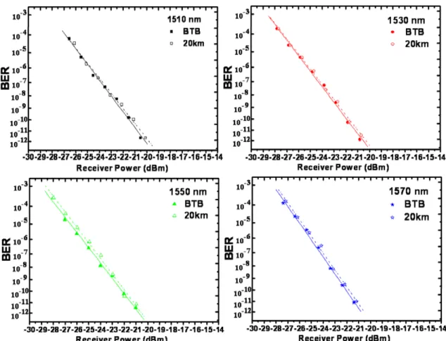
The optical powers of the downstream channel were from -1.86 to -1.23 dBm and launched into the network simultaneously. The back-to-back (BTB) transmitted optical eye patterns are shown in Fig. 3(a). The OC-192 eye mask margins distributed from 14 to 18% and the jitters were from 15.1 to 17.4 psec. To achieve the best performance, the bias and modulation condition of the LiNbO3 modulator has been optimized for each channel. Fig. 3(b) shows the received and reshaped eye patterns after a 20-km SMF transmission by a homemade APD-TIA optcal receiver. The OC-192 eye mask margins distributed from 37 to 40%, which were improved by the limiting amplifier. The jitters were from 9.7 to 10.7 psec, which were degraded by the dispersion effect in the SMF and the optical receiving circuit. Values of the launched power, the OC-192 eye mask margin, and the jitter for every channel are summarized in Table1.
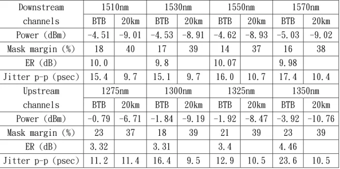
The optical sensitivities were measured by connecting the output ports of the CWDM demultiplexer with a variable optical attenuator and a homemade optical receiver. Optical sensitivities of the BTB connection were around -22.91 dBm and degraded to about –22.22 dBm after 20 km SMF transmission by APD-TIA receiver, as shown in Fig. 4. The power penalty distributed from 0.19 to 0.27 dB. This degradation is mainly due to the SMF dispersion effect and has been minimized by the external modulation approach. With –22 dBm APD-TIA receiver sensitivity to ensure an error-free operation in practical systems, -1.42 dBm average modulated laser power gives rise to a power budget of 11 dB, which allows transmission over 20 km of standard SMF without optical amplifiers. The total optical power loss of the downstream path with 20 km SMF in this experimental setup is 8.55, 9.08, 9.34, and 10.21 dB for the wavelengths of 1510, 1530, 1550, 1570 nm, respectively. In our elementary experiment, the power budget is about 12 dB and it’s enough to afford a ratio of 1:16 splitting network. If the modulated input power is above 3 dBm and using a commercial APD-TIA optical receiver, the power budget will be over 16 dB and the sensitivities will be increased easily. Therefore, the splitting ratio could achieve a ratio of 1:32 for each channel. The related values and monitoring power points are summarized in Table 2 and Table 3.
3.2 Upstream transmission results
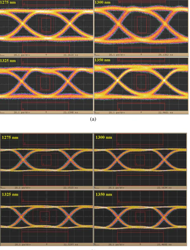
The DFB-LDs opical powers of the upstream channels were from 4.22 to 2.73 dBm and launched into the CWDM multiplexer simultaneously. Fig. 5(a) shows eye patterns for the BTB connection, The OC-192 eye mask margins distributed from 18 to 23% and
the jitters were from 11.2 to 23.6 psec. The received and reshaped eye patterns after a 20-km SMF transmission by a homemade APD-TIA receiver are shown in Fig. 5(b). The measured eye pattern maintained at a clearly open figure and could ensure a good transmission. Values of the optical power, OC-192 eye mask margin, and the jitters for every channel are summarized in Table 1.
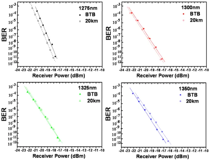
The optical sensitivity was measured by connecting the output port of the CWDM demultiplexer with a variable optical attenuator and a homemade optical receiver, as shown in Fig. 6. As summarized in Table 2, the BTB receiving sensitivity of upstream channels distributed from -18.20 to -18.42 dBm. The receiving sensitivities of longer wavelength channels were better than shorter wavelengths due to a higher quantum efficiency of the photodiode used in the homemade optical receiver. The received sensitivity after a 20 km SMF transmission was from -17.68 to -18.73 dBm. The power penalty was only several tenth of a dB for all four channels and was slightly larger than the downstream channels due to the direct modulation scheme. This is due to a larger dispersion of optical fiber from the larger spectral bandwidth of direct modulation sources. On the other hand, although the dispersion coefficient is larger at the longer wavelengths, since the downstream signal is external modulated, so the dispersion is smaller and the results of a neglible power penalty compared with upstream signals. In addition, the total optical power loss of the upstream path in this experimental setup is 12.41, 12.24, 11.22, and 12.84 dB for the wavelengths of 1275, 1300, 1325, 1350 nm, respectively. With –19 dBm APD-TIA receiver sensitivity to ensure an error-free operation in the practical systems, 3.24 dBm average modulated laser power gives rise to a power budget of 10 dB, which allows transmission over 20 km of standard SMF without optical amplifiers. In our elementary experiment, the power budget was about 9 dB and was adequate to afford a ratio of 1:8 splitting network. Although the dispersion coefficient is larger at the longer wavelengths, since the downstream signal is externally modulated, the dispersion is smaller and results a neglible power penalty compared with upstream signals. Furthermore, we have evaluated approximate power penalties due to LD chirp with 10 Gb/s data rate in DFB-LDs wavelengths from 1275 to 1350 nm for SMF transmission. The computed power penalties of the upstream channels could match with the measured results. The receiving sensitivity of this CWDM-PON system could be improved further if the output power of DFB lasers were increased several dB or a commercial APD-TIA receiver was used. Therefore, it would be possible to construct the proposed network. The burst mode operation did not adequate in this experiment due to the limited component performance. Additionally, we have observed the pulse compression effect which gives rise to a negative dispersion penalty due to a low chirp of the laser. To get of this effect, the DFB laser wavelength needs to be properly selected and its range is found to be as wide as 40 nm for transmission over 20 km standard SMF.
4. Discussion of modulated lasers and transmission characteristics
and directly modulated lasers are operated at 10 Gb/s in unrepeatered systems for 1.3 and 1.5 μm wavelength regions are the major concerns. Usually, a high-bit-rate and long-reach transmission presents dispersion-related impairments. Therefore, the downstream signals with 1.5 μm wavelength are designed by externally modulated sources. Because the client side cannot afford the costly external modulation source, adopt the directly modulated 1.3 μm DFB-LD at a lower cost for upstream signals.
4.1 Dispersion Penalties for Externally Modulated Lasers
A low-chirp 1.5 μm externally modulated laser source is the most applicable to unrepeatered transmission over 50 km. A CW laser source has enough high power to compensate for the excessive modulation loss and the broaden linewidths of laser to limit dispersion penalties [13]. For instance, there is only a 2 dB penalty for 100 km SMF transmission at 5 to 10 Gb/s for systems operating at 1.55 μm with 15 ps/km·nm of chromatic dispersion [10]. Therfore, 1.5 μm externally modulated laser sources are easy to acquire the downstream channels that they are installed in Metro/Access applications of transmission distance between 20 and 40 km.
4.2 Dispersion Penalties for Directly Modulated Lasers
On the other hand, a low-cost 1.3 μm directly modulated lasers source is able to applicate in upstream channels of the client side. Although the standard SMF exhibits a zero dispersion point at the wavelength of 1.31 μm, the power penalty induced by the chromatic dispersion is a critical issue for the upstream signal around 1.31 μm running at 10 Gb/s [11, 14, 15]. For the calculation of the group delay difference between wavelengths, the chromatic dispersion coefficient is obtained from the following equation (1) [16, 17].
d d d d c D 2 2 1 (1)
where c and λ are the velocity of light in free space and the wavelength of the LD, respectively. The behavior of the linear material dispersion coefficient D for
a standard SMF is shown in Fig.7. The wavelength λ0 is approximately 1.314 μm, and the dispersion at 1.5 μm is approximately 13.85 to 17.2 ps/km·nm. The chromatic dispersion coefficients are calculated to be the values of -3.511, -1.223, 0.934, and 2.974 ps/km·nm for the wavelengths of 1275, 1300, 1325, 1350 nm, respectively. The calculated chirp power penalties due to LD chirp and fiber chromatic dispersion were analyzed by Yamamoto, et al. [18, 19]. The change of the eye amplitude is due to the LD chirp, and it is approximated by (2). The power penalty
2 2 2 2 2 2 2 ln 2 ) 4 3 2 ( X B c L X X , and X DBL (2)
where the is the spectrum linewidth of the DFB-LD, B is the transmitted bit-rate, and L is the transmission distance. The spectrum linewidths of the
DFB-LDs modulated at 10 Gb/s with current of 50 mA are measured by an optical spectrum analyzer (resolution 0.01 nm). The spectral linewidth were 0.112, 0.141, 0.115, and 0.138 nm for the wavelengths of 1275, 1300, 1325, 1350 nm, respectively.
The power penalty is estimated by the degradation of signal-to-noise ratio (SNR) due to the decrease of the signal amplitude and is expressed by the following equation (3). ) 1 log( 1 2 10 x x ty PowerPenal (3)
where x is the excess noise factor of the APD and is about 0.8 for an InGaAs-APD
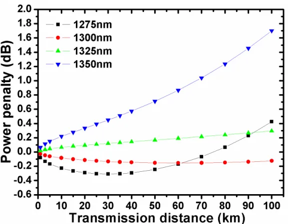
optical receiver. The relation between dispersion power penalties and SMF transmission distances with 10 Gb/s operation for various wavelengths are calculated and plotted in Fig. 8. It is shown that the dispersion power penalty is less than 0.6 dB for a 40 km SMF transmission with wavelength distributed from 1275 to 1350 nm. Furthermore, the relation between dispersion power penalties and operating wavelengths with 10 Gb/s operation and 20 km SMF transmission are calculated and plotted in Fig. 9. The DFB-LDs linewidths are assumed to be varied between 0.10 and 0.25 nm. The experimental results of the power penalties with different wavelengths are shown as solid dots in Fig. 9. The computed power penalties of the upstream channels matched well with the measured results. Both the calculated and experimental results confirm that the DFB-LDs with wavelength range of 1275 nm to 1350 nm at 10 Gb/s operation have neglible power penalties in this proposed CWDM-PON system.
5. Conclusion
A bidirectional CWDM-PON system with a symmetric 40 Gb/s data rate for 20 km SMF transmission has been demonstrated. The maximum subscribing bit rate of each client could be adjusted from a gigabit to 10 Gb/s and the split ratio could reach to 1:128. Four downstream channels with externally modulated light sources emitting at wavelengths from 1510 to 1570 nm and four upstream channels with directly modulated DFB-LD emitting at wavelengths from 1275 to 1350 nm were adopted to minimize the dispersion effect of SMF transmission. All the downstream and upstream channels were operated at 10 Gb/s simultaneously to demonstrate the 40 Gb/s fully duplex transmission. The power penalties of directly modulated DFB-LD are extensively studied and are confirmed to be neglible in this proposed CWDM-PON system. Although the dispersion coefficient is larger at the longer wavelengths, since the downstream signal is external modulated, therefore the dispersion power penalty is neglible, too. Utilizing the simple low-cost CWDM architecture, the matured 10 Gb/s module technology, moderate transmission distance, and the potential for a large splitting ratio, this CWDM-PON access network has promising potential characteristic to apply at the highspeed local-area-networks (LAN) and next generation FTTH networks.
REFERENCES
1. S. J. Park, C. H. Lee, K. T. Jeong, H. J. Park, J. G. Ahn, and K. H. Song: J. Lightwave Technol. 22 (2004) 2582.
2. S. M. Lee, M. H. Kim, and C. H. Lee: J. Lightwave Technol. 22 (2004) 2623. 3. O. Akanbi, J. Yu, and G. K. Chang: IEEE Photon. Technol. Lett. 18 (2006) 340. 4. W. Yue, J.V. Mocerino: in Proc. Optical Fiber Communication Conf., (OFC), Mar.
(2007) JthA86.
5. M. Abrams, P. C. Becker, Y. Fujimoto, V. O’Byrne, and D. Piehler: J. Lightwave Technol. 23 (2005) 236.
6. F. Munoz, P. Benitez, O. Dross, J. C. Minano, and B. Parkyn: J. Lightwave Technol.
24 (2006) 4568.
7. J. Yu, O. Akanbi, Y. Luo, L. Zong, T. Wang, Z. Jia, G. K. Chang: IEEE Photon. Technol. Lett. 19 (2007) 571.
8. S. M. Lee, M. H. Kim, and C. H. Lee: IEEE Photon. Technol. Lett. 19 (2007) 405. 9. G. C. Gupta, M. Kashima, H. Iwamura, H. Tamai, T. Ushikubo, and T. Kamijoh: J.
Lightwave Technol. 25 (2007) 193.
10. A. F. Elrefaie, R. E. Wagner, D. A. Atlas, and D. G. Daut: J. Lightwave Technol.
6 (1988) 704.
11. I. Kim, T. J. Miller, and Y. K. Park: IEEE Photon. Technol. Lett. 9 (1997) 1167. 12. T. T. Shih, M. C. Lin, and W. H. Cheng: IEEE J. Select. Topics Quantum Electron.
12 (2006) 1009.
13. K. Morito, R. Sahara, K. Sato, and Y. Kotaki: IEEE Photon. Technol. Lett. 8 (1996) 431.
14. W. P. Huang, X. Li, C. Q. Xu, X. Hong, C. Xu, and W. Liang: J. Lightwave Technol.
25 (2007) 11.
15. G. P. Agrawal, Nonlinear Fiber Optics, 3rd ed.
16. A. Sugimura, K. Daikoku, N. Imoto, and T. Miya: IEEE J. Quantum Electron. QE-16 (1980) 215.
17. R. A. Linke: IEEE J. Quantum Electron. 16 (1985) 593.
18. S. Yamamoto, M. Kuwazuru, H. Wakabayashi, and Y. Iwamoto: J. Lightwave Technol.
5 (1987) 1518.
19. F. Koyama and Y . Suematsu: IEEE J. Quantum Electron. QE-21 (1985) 292. 20. J. C. Campbell: J. Lightwave Technol. 6 (1988) 564.
Table I. The measured parameters of eye pattern. Downstream 1510nm 1530nm 1550nm 1570nm channels BTB 20km BTB 20km BTB 20km BTB 20km Power (dBm) -4.51 -9.01 -4.53 -8.91 -4.62 -8.93 -5.03 -9.02 Mask margin (%) 18 40 17 39 14 37 16 38 ER (dB) 10.0 9.8 10.07 9.98 Jitter p-p (psec) 15.4 9.7 15.1 9.7 16.0 10.7 17.4 10.4 Upstream 1275nm 1300nm 1325nm 1350nm channels BTB 20km BTB 20km BTB 20km BTB 20km Power (dBm) -0.79 -6.71 -1.84 -9.19 -1.92 -8.47 -3.92 -10.76 Mask margin (%) 23 37 18 39 21 39 23 39 ER (dB) 3.32 3.31 3.4 4.46 Jitter p-p (psec) 11.2 11.4 16.4 9.5 12.9 10.5 23.6 10.5
TableII. The measured optical power and sensitivity values. Downstream channels 1510nm 1530nm 1550nm 1570nm Launch power at node A2
(dBm) -1.86 -1.28 -1.23 -1.28 BTB sensitivity (dBm) -22.22 -22.67 -22.91 -22.75 Received power at node E2
(dBm) -9.01 -8.91 -8.93 -9.02 20-km Receiving sensitivity (dBm)-22.01 -20.48 -22.64 -22.51 Power penalty (dB) 0.21 0.19 0.27 0.24 Splitting ratio3
(estimated) 1:4 1:4 1:4 1:4 Maximum splitting ratio4
(estimated) 1:32 1:32 1:32 1:32 Upstream channels 1275nm 1300nm 1325nm 1350nm Launch power at node F5
(dBm) 4.22 3.28 2.74 2.73 BTB sensitivity (dBm) -18.22 -18.42 -18.27 -18.20 Received power at node I5
(dBm) -7.09 -8.04 -8.02 -9.92 20-km Receiving sensitivity (dBm) -18.73 -18.72 -18.17 -17.68 Power penalty (dB) -0.51 -0.30 0.102 0.57 Splitting ratio3
(estimated) 1:4 1:4 1:4 1:4 Maximum splitting ratio4
(estimated) 1:32 1:32 1:32 1:32 1. Power unit in dBm, sensitivity was measured at bit error rate of 10-9
2. Output power was measured at node-A, Received power was measured at node-E for downstream path (as shown in Fig.2)
3. The splitting ratio was estimated based on experimental results 4. Adopting the self-made 10 Gb/s APD-TIA receiver
5. Output power was measured at node-F, Received power was measured at node-I for upstream path (as shown in Fig.2)
TableIII. The monitoring points of optical power. Downstream channels A B C D E 1510-nm 1.86 2.41 6.91 7.54 9.01 1530-nm 1.28 1.81 6.19 6.75 8.91 1550-nm 1.23 1.84 6.15 6.64 8.93 1570-nm 1.28 1.93 5.92 6.49 9.02 Upstream channels F G C B H I 1275-nm 4.22 1.76 1.43 -4.87 -5.18 -7.09 1300-nm 3.28 0.73 0.47 -5.73 -6.08 -8.04 1325-nm 2.74 1.09 0.77 -5.33 -5.76 -8.02 1350-nm 2.73 0 -0.49 -6.49 -6.91 -9.92 1. Power unit in dBm.
2. Output power was measured at node A, B, C, D, E for downstream path (as shown in Fig.2)
3. Output power was measured at node F, G, C, B, H, I for upstream path (as shown in Fig.2)
Fig.1. A schematic diagram of the proposed bi-directional CWDM-PON system.
(a)
(b)
Fig.3. The measured eye pattern of downstream channels for the (a) back-to-back, (b) received and reshaped by optical receiver after a 20 km SMF transmission. (20.1 ps/div)
Fig. 4. The sensitivities of the downstream channels for back-to-back and 20 km SMF transmission.
(a)
(b)
Fig. 5. The measured eye patterns of 10Gb/s upstream channels for the (a) back-to-back, (b) received and reshaped by optical receiver after a 20 km SMF transmission. (20.1 ps/div)
Fig. 6. The sensitivities of the upstream channels for back-to-back and 20 km SMF transmission.
Fig. 8. The calculation of power penalty versus transmission distance for upstream wavelengths.
Fig. 9. The power penalty versus wavelength of the calculated curve and distributed measurement values for 20 km SMF transmission.
國科會補助專題研究計畫項下出席國際學術會議心得報告
日期: 99 年 10 月 30 日一、參加會議經過
SPIE 是一個自從 1955 年創立的國際性專門從事光學與光子技術研究的協會。出
版多份技術與市場刊物與書籍,每年並舉辦多場研討會,聚集各國專家發表最新研
究成果並進行交流,這些研討會中除專門針對特定領域或地區外,有 Photonics West、
Photonics Asia、與 Photonics Europe 等在美國、亞洲與歐洲舉辦的大型研討會。
本次參加的 SPIE Photonics Europe 在比利時的布魯塞爾舉辦,包含 19 個主要會議,
共計 1300 篇論文發表,約 5000 位人員參加,是一場大型的國際研討會。
因為台灣沒有直飛比利時布魯塞爾的定期班機,所以由台灣先搭華航班機飛到法
國巴黎,再轉搭歐洲之星高速火車往比利時布魯塞爾,火車約每小時都有一班直達
列車,比轉搭飛機方便也比較節省費用。因為這次有許多會議同時舉行所以必須選
擇特定主題參加,本次主要參加與論文發表會議是(編號 7720) Semiconductor
計畫編號
NSC96-2221-E-151-024-MY3
計畫名稱
40Gbps 光收發器與分波多工被動式光網路系統之應用
出國人員
姓名
施天從
服務機構
及職稱
國立高雄應用科技大學
電子工程系副教授
會議時間
99 年 4 月 12 日至
99 年 4 月 16 日
會議地點
比利時布魯塞爾
會議名稱
(中文)SPIE 歐洲光電研討會
(英文)SPIE Photonics Europe
發表論文
題目
(中文)光通訊同軸式雷射封裝的 25-GHz TO-can 基座
(英文) A 25-GHz TO-Can Header for Coaxial Laser Package on
Transmission Applications
lasers and Laser Dynamics。另本次大會在每天特定時間有特別舉辦”Hot Topics
in Photonics”的報告,主題有下列各項,非常值得參加以瞭解 Phtonics 領域最新
技術與研究狀況:European photonics research strategy、 Optical nanoscopy、
Micromanipulation、 Photonics and computing、 Photonic integration、
Nanophotonics、 Plastic photonics and electronics、 Ultrafast nonlinear
optics。
返程時遇到冰島火山爆發,導致大部分歐洲機場關閉,而延宕五天返國。
二、與會心得
主要參加的 Semiconductor lasers and Laser Dynamics 會議中,包含有 VCSEL、
Laser Chaos Applications、Laser array、Mode-Locking、Nanolasers、Quantum Dots
等主題。有討論 40-Gb/s 的 850nm VCSEL,由瑞典、德國、愛爾蘭與英國等研究機構
共同發表。美國 Finisar 公司發表二維 VCSEL array,總傳輸速率 1000-Gbps。瑞士
Ecloe Polytechnique Federale de Lausanne 發表 1310nm 的 VCSEL array 等。
本次所舉行的展覽共有約 150 家廠商參加,相關照片如附。比較特別的是有許多
歐洲公司參加,可以廣泛接觸各式各樣與歐洲各國的零組件供應商,例如俄羅斯或
德國等。
三、考察參觀活動(無是項活動者略)
無
四、建議
1. 歐洲議會提供整合性大型計畫的資助,在光通訊領域持續鎖定高傳輸容量與積
體光學等技術研究。計畫合作成員有學校、研究機構與公司法人,研究經費可達每
年數百萬歐元。相對於台灣除科學園區固本精進計畫針對學校與公司補助外,則較
無此種整合性大型計畫,建議可成立跨經濟部、國科會、教育部的基金,針對特定
主題進行研發計畫的支持。
2. 歐洲在光通訊雷射部分,非常著重於 VCSEL 的研究,基本上在短距離傳輸時
VCSEL 具有成本與性能的優勢;另為達成更高容量傳輸,歐洲也持續進行 PLC 或積體
化研究。但台灣目前已經少有類似元件之研發,建議鼓勵學界持續研發以跟進,避
免相關技術產生斷層。
五、攜回資料名稱及內容
1. 會議議程一本
2. Semiconductor lasers and Laser Dynamics IV 論文集一本(SPIE Vol. 7720)
六、其他
A 25-GHz TO-Can Header for Coaxial Laser Package on Transmission
Applications
Tien-Tsorng Shih*a, Pei-Hao Tsengb, Hao-Wei Chena, Sung-Mao Wuc, Wood-Hi Chengb
a
Dept. of Electronics Engineering, National Kaohsiung University of Applied Sciences, 415 Chien Kung Rd., Kaohsiung, Taiwan;
b
Dept. of Photonics, National Sun Yat-sen University, 70 Lianhai Rd., Kaohsiung, Taiwan; cDept. of Electrical Engineering, National Kaohsiung University, 700 Kaohsiung University Rd., Kaohsiung, Taiwan
ABSTRACT
A new 5-pin transistor outline (TO-Can) header for conventional coaxial laser package has been proposed and demonstrated by using a three-dimensional full-wave electromagnetic simulation tool. The applicability of the simulation tool was verified by a measurement result of a conventional TO-56 header. By adopting a two-session feed-through via and a bent feed-lead, this TO-Can header has the optimal impedance for high-speed modulation. The reflection loss can be controlled beneath –10-dB before 15-GHz with a 50-Ω termination. The 3-dB modulated bandwidth with a load impedance of 5-Ω and 50-Ω is over 23-GHz and 37-GHz, respectively. This TO-Can header provides a low-cost coaxial laser package solution with widely load impedances from 5-Ω to 50-Ωand may apply in the emerging 100-Gigabits Ethernet (100GbE) and next generation Fiber Channel (20GFC) applications.
Keywords: 100-Gigabits Ethernet, Fiber Channel, 100GbE, 20GFC, TO-Can, coaxial laser package, TOSA
1. INTRODUCTION
Currently, the 100-Gigabits Ethernet (100GbE) network based on four-channel wavelength division multiplexing (WDM) technology has been discussed extensively [1]-[3]. In the same time, the 21-Gb/s Fiber Channel (20GFC) has attracted much attention and plays an important role in the storage area network. A low cost laser module is very essential for these applications. Although low-cost 10-Gb/s transmitter optical sub-assembly (TOSA) modules by adopting coaxial TO-Can laser package technology have been demonstrated [4]-[9], however, these TOSAs have still a limited data rate of 10-Gb/s in common and cannot be applied in the future 100GbE and 20GFC networks. Nowadays, laser diode (LD) fabrication technology is advanced and the modulation bandwidth over 20-GHz have been demonstrated [10]-[13], so the limited modulation bandwidth of the TOSA is due to the low-cost coaxial TO-Can laser package technology. Therefore, breaking the bandwidth limitation and providing a cost effective approach is very important for future 100GbE and 20GFC networks. In order to analysis the high-frequency characteristics of a TO-Can structure in details, we construct and calculate the electromagnetic model of a conventional TO-56 header by using the High-Frequency Structure Simulator (HFSS) software. The HFSS software is a three-dimensional (3D) full-wave electromagnetic simulation tool that takes the 3D geometric structure and material parameters of microwave characteristics into account. To check the applicability of the simulation approach, the reflection loss (S11) measurement of an opened circuit of a conventional TO-56 header has been implemented. The measured result and the simulated result have good consistency at a frequency up to 20-GHz. Through the HFSS simulation, an electrical field diagram is presented at high frequency. After a comprehensive study on the TO-56 header, the bottleneck of the limited data rate of a TOSA has been attributed as the impedance variation of the feed-through via and the feed-lead of the TO-56 header. By optimizing the geometry of the feed-through via and the feed-lead of the TO-Can header, a new 5-pin TO-Can header with a two-session feed-through via and a bent feed-lead for high-speed modulation is proposed and demonstrated. This 5-pin TO-Can header has a 3-dB modulated bandwidth over than 24-GHz with different load impedances of 5-Ω
to 50-Ω in general and provides a low-cost solution for traditional coaxial laser package which can be applied in the emerging 100GbE and 20GFC networks.
2. SIMULATION APPROACH AND VERIFICATION
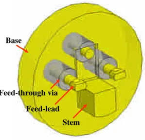
A conventional 4-pin TO-56 header is used to verify the applicability of HFSS simulation approach. A schematic drawing of the TO-56 header is shown in Fig. 1(a). The diameter of the feed-lead is 0.45-mm and the diameter of the feed-through via is 1 mm. The feed-lead can be divided into three parts: the outside feed-lead, the coaxial feed-lead, and the inside feed-lead, as shown in Fig. 1(b). The relative dielectric constant (εs), relative permeability (μs), and electric conductivity (σ) of metal materials are principal parameters in calculating the characteristic impedance at high frequency. The surfaces of header base and feed-line are plated with a 1-μm thick gold film and the current waves flow through the surface at high frequency. Therefore, we only consider gold as the conduction metal [14]. The parameters of gold were set εsat 1, μsat 0.9996, and σat 4.1·107-S/m, respectively. The feed-through via is filled with a sealed glass to insulate the coaxial feed-lead and the header base. The relative dielectric constant (εs) of the sealed glass is 5.5. A 3D electromagnetic model of the TO-56 header by using HFSS software is constructed according to the specification of a TO-56 header.
Feed-lead Stem Feed-through via
Base
L1: Outside feed-lead L2: Coaxial feed-lead L3: Inside feed-lead R: Feed-through via
L3
L1
L2 R
(a) The 3D view (b) The cross-sectional view
Fig. 1. Configurations of the conventional TO-56 header.
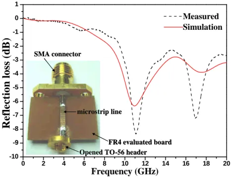
To verify the applicability of the HFSS simulation approach, an opened circuit measurement of a TO-56 header has been implemented. The outside feed-lead of a TO-56 header is cut as short as possible and attaches to a 50-Ω microstrip lineof a FR4 evaluated board by soldering. The bottom side of the evaluated board is connected with the base of the TO-56 header. The other side of the evaluated board has an SMA connector. The physical length of the microstrip line on the evaluated board corresponds to three quarters of wavelength at 10-GHz giving a broadband impedance matching between the outside feed-lead of the header and the evaluated broad. No any object put in the stem of the TO-56 header, which is equivalent as an opened circuit of the terminal end. The modulated signal feeds from the SMA connector and injects into the TO-56 header through feed-leads. The stem and the base of the TO-56 header are the return ground path. The inset of Fig. 2 shows a practical photograph. It’s a single-end configuration. A 20-GHz Vector Network Analyzer (VNA) is used to measure the reflection loss. The measured result is shown as the dotted line of Fig. 2. The first resonance frequency is 11.1-GHz and the return loss is -8.3-dB. The second resonance frequency is 17-GHz. The simulated result is shown as the solid line of Fig. 2. The first resonance frequency is 10.95-GHz. The resonance frequency is consistent for both the measured and simulated results. However, the simulated amplitudes of return loss are slightly different from the measured result. This difference might come from the input impedance mismatch, insertion loss, and material loss of the FR4
evaluated board and SMA connector in measuring the high-frequency characteristics. By adopting the de-embedded action can eliminate these influences. Unfortunately, our VNA has not this de-embedded function. In general, the simulated result shows a good agreement with the measured result in the measuring frequency range of 20-GHz.
Opened TO-56 header FR4 evaluated board SMA connector
microstrip line
Opened TO-56 header FR4 evaluated board SMA connector microstrip line 0 2 4 6 8 10 12 14 16 18 20 -10 -9 -8 -7 -6 -5 -4 -3 -2 -1 0 1
R
e
fl
e
ct
io
n
lo
ss
(d
B
)
Frequency (GHz) Measured SimulationFig. 2. The simulated and measured S11 curves for an opened TO-56 header.
3. HIGH-FREQUENCY CHARACTERISTICS OF THE FEED-LEAD
Based on the structure of the TO-56 header, as shown in Fig. 1(b), the feed-lead can be divided into three parts and the high-frequency characteristics are discussed separately. The outside feed-lead (L1) and the inside feed-lead (L3) could be taken as a cylindrical line. The coaxial feed-lead (L2) and the feed-through via (R) could be considered as a coaxial line [8, 15].
A. Frequency characteristics of the cylindrical line
As increasing the length of the feed-lead, the inductance of the feed-lead is increased. The increased inductance would limit the bandwidth of the TO-Can header. In order to ensure a maximum bandwidth, feed-lead length should be designed as short as possible. The parasitic inductance (L) of round lead is expressed as equation (1).
7 1 2 2 10 1 1 ln 2 r l r l r l r l l L S [H] (1)
where l and r are the length and the radius of feed-lead, respectively [15]. The length of outside feed-line can be reduced to a minimum value by adopting a flexible PCB [16]. However, the inductance of inside feed-lead is much complex. The rough frequency characteristics can be estimated through an equivalent circuit model [8, 15]. However, the advanced frequency characteristics of the cylindrical line should be calculated by solving the boundary conditions of a 3D electromagnetic wave. B. Frequency characteristics of the coaxial line.
The parasitic capacitance, parasitic inductance, and the characteristic impedance (Z0) of a coaxial line can be expressed by the
following equations [14, 15, and 17]:
l a b C S ln 20 [F] (2)
l a b C z L ln 2 0 2 0 [H] (3) S a b Z 0 0 0 ln 2 1 [Ω] (4)
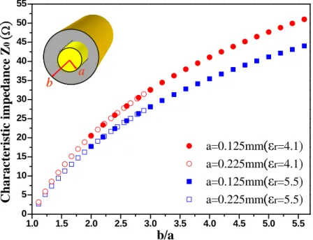
where ε0is the permittivity in free space, εsis the relative dielectric constant of sealed glass, b is the radius of feed-through via, a is the radius of feed-lead, l is the length of coaxial line, and μ0 is the permeability in free space, respectively. For a conventional TO-56 header, a is 0.225-mm, b is 0.5-mm, and εsis 5.5. The theoretical Z0is calculated to be only 20.4-Ω,which isnotmatch with
the standard 50-Ω requirement.TheZ0 can be increased by increasing the radius of feed-through via, decreasing the radius of
feed-line, or decreasing the relative dielectric constant of sealed glass. To preserve a good hermetic performance of a TO-Can header, the sealed glass is limited within a few options. For a commercial available consideration, the lowest relative dielectric constant of sealed glass is 4.1. If we take account of the limitation of a conventional TO-56 header manufacturing process, the minimum radius of feed-lead is 0.125-mm. A feed-lead with a radius less than 0.125-mm is not a practical design. Due to a tight space requirement of TO-Can header, the radius of feed-through via is limited to be around 1.4-mm. Therefore, the maximum b/a values of feed lead with radius of 0.225-mm and 0.125-mm are limited at 3.1 and 5.6, respectively. By combining all the practical issues, the relation between Z0and those parameters is shown in Fig. 3. The maximum Z0of a feed-lead with a radius of 0.225-mm
can achieve only 33-, as shown as the circles and squares in the figure. If the radius of the feed-lead reduces to 0.125-mm, then the maximum Z0 can be increased to approximate 50-Ω, as shown as the solid dotes and solid squares. Therefore, to adopt a small
feed-lead and a sealed glass with lower dielectric constant is important to design a 50-impedance matched TO-Can header.
a b a b 1.0 1.5 2.0 2.5 3.0 3.5 4.0 4.5 5.0 5.5 0 5 10 15 20 25 30 35 40 45 50 55 a=0.125mm(
ε
r=4.1) a=0.225mm(ε
r=4.1) a=0.125mm(ε
r=5.5) a=0.225mm(ε
r=5.5) b/a C h a r a c te r is ti c im p ed a n c e Z 0(
)
Fig. 3. The relation of Z0and related parameters of coaxial line.
4. PROPOSAL OF A NEW 25-GHZ TO-CAN HEADER
Fig. 4 illustrates the structure of the new 5-pin TO-Can header at (a) the 3D configuration and (b) cross-sectional view. The pin-1 and pin-3 are feed-leads for input signal path, pin-2 is used for monitor diode output, and pin-4 and pin-5 are ground leads for laser diode’ssignalreturn path.The signal passed through the inside feed-lead over the stem without an enough flat ground plane is a major drawback of a TO-56 header. Therefore, this new TO-Can header has a wide stem to maintain the wire-over-ground transmission of the inside feed-lead. Besides, a large stem will benefit the thermal dissipation. The radius of the feed-lead is 0.125-mm. The distance between the center of feed-lead and the stem is 0.29-mm. In the coaxial feed-lead portion, a two-section
feed-through via of different diameter is proposed especially. The first-section of the feed-through via (R1) has a radius of 0.48-mm and is filled with a low dielectric constant sealed glass. The thickness of the first section of the feed-through via is 0.6-mm. The second-section of feed-through via (R2) has a radius of 0.29-mm and the thickness is 0.3-mm. This section is hollow to insulate the feed-lead from the header. The inside feed-lead is designed as a 90-degree bent shape to shorten the length of bonding wires between the feed-lead and the laser diode chip. Because we intend to utilize this TO-Can header under load impedances of 5 to 50-Ω, above dimension is an optimum result. However, by adjusting the R1, R2, and the distance between the center of feed-lead and the stem, the impedance can match with specific load impedance further.
Feed-through via (R2) Stem Base Feed-lead Feed-through via (R1) Feed-through via (R2) Stem Base Feed-lead Feed-through via (R1) R2 R1
Pin-1 Pin-2 Pin-3
Pin-4 Pin-5
R2 R1
Pin-1 Pin-2 Pin-3
Pin-4 Pin-5
(a) (b)
Fig. 4. Structure of the new TO-Can header (a) the 3D view and (b) the cross-sectional view.
5. ANALYSIS AND COMPARISON OF THE NEW TO-CAN HEADER AND CONVENTIONAL TO-56 HEADER
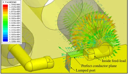
The electrical characteristics of the new TO-Can header and a convention TO-56 header with the electrical field diagrams and S-parameters by using HFSS is simulated and analyzed. The simulated configurations and the electrical field diagrams of the new TO-Can header and the TO-56 header are shown in Fig. 6(a) and (b), respectively. A lumped port is inserted at the center of the header to represent the load. The lumped port directly links to the stem of the electrical ground. We can simulate the situations of different load by varying the impedance of lumped port. A perfect conductor plane is placed between the inside feed-lead and the lumped port to conduct the electrical signal. In a real case, bonding wires are used to connect the inside feed-lead and the load. Bonding wires induce parasitic inductance and degrade the electrical characteristics. However, the appearance of bonding wires will blur the inherent performance of the header. So the bonding wires are replaced by a perfect conductor. The operating frequency and the load are set at 15-GHz and 50-Ωin the simulation of Fig. 6. The discretized vectors of the electrical field distribution are both TEM mode in the coaxial feed-lead. The intensity of electrical field of the TO-56 header is apparently small and weak than the new TO-Can header. Because the TO-56 header has a bigger drop of impedance between the coaxial feed-lead and the inside feed-lead, the power of microwave propagation is sharply reduced. However, the impedance discontinuity of the new TO-Can header has minimized between the coaxial feed-lead and the inside feed-lead. The microwave power can be propagated completely in the two-section coaxial feed-lead. Therefore, the intensity of electrical field of the new TO-Can header is apparently stronger than the TO-56 header in the coaxial feed-lead. The impedance matching of coaxial feed-lead of the new TO-Can header has a significant improvement for electrical field propagation.
Inside feed-lead Perfect conductor plane Lumped port
(a)
Inside feed-lead Perfect conductor plane Lumped port
(b)
Fig. 5. Electrical field diagrams of (a) the proposed new TO-Can header and (b) the conventional TO-56 header
By referring the intrinsic electrical equivalent circuit, the rise and fall of imaginary impedance of a laser diode in high frequency is negligible compared with the real impedance [7, 8, 18]. Therefore, the impedance of laser diode is only considering real part in this study. Usually, the load impedance inside a coaxial TOSA has different values. When there is no external matching resistor, the load is the impedance of the laser diode only and can be presented by a few Ohms [7, 8]. To have a better impedance matching result, researchers will insert external matching resistors and the load impedance is increased from a few Ohms to 25-Ω or50-Ω [6-8]. Therefore, we set both 5-Ω and 50-Ω astheload impedancein thesimulation ofS-parameters. The simulated reflection loss, insertion loss, and the phase curves of S21 of the new TO-Can header and conventional TO-56 header are shown in Fig. 7 (a), (b), and (c), respectively. The simulated reflection loss of new TO-Can header can be controlled beneath –10 dB with a load of 50-Ω before 15-GHz. The 3-dB transmission bandwidth of the new TO-Can header achieves over than 23-GHz and 37-GHz with a load of 5-Ωand 50-Ω, respectively, while the 3-dB transmission bandwidth of the TO-56 header is only 15-GHz. The linear region of the phase curves of the new TO-Can header is better evidently compared with the conventional TO-56 header. It’salmostadouble increment of a conventional TO-56 header.
0 5 10 15 20 25 30 35 40 -40 -35 -30 -25 -20 -15 -10 -5 0 TO-56 header 50 5
New TO-can header 50 5 R e fl e ct io n lo ss [S 1 1 ] (d B ) Frequency (GHz) 0 5 10 15 20 25 30 35 40 -18 -16 -14 -12 -10 -8 -6 -4 -2 0 TO-56 header 50 5
New TO-can header 50 5 T ra n sm is si o n lo ss [S 2 1 ] (d B ) Frequency (GHz) (a) (b) 0 5 10 15 20 25 30 35 40 -250 -200 -150 -100 -50 0 50 100 150 200 250 TO-56 header 50 5
New TO-can header 50 5 P h a se [S 2 1 ] (d B ) Frequency (GHz) (c)
Fig. 7. The simulation results of S-parameters for the new TO-Can and the conventional TO-56 header with loads of 5-Ω and 50-Ω.(a) The S11 curves, (b) the S21 curves, and (c) the phase curves of the S21
6. CONCLUSION
In summary, a new TO-Can header for the low-cost coaxial laser package has been proposed and demonstrated by a 3D full-wave electromagnetic simulation. The applicability of the simulation tool has been verified with an experimental result. The reflection loss, insertion loss, and phase of this TO-Can header show significant improvements by comparing with the conventional TO-56 header. The simulated reflection loss is beneath –10-dB under 15-GHz at a 50-load impedance, the 3-dB modulated bandwidth achieves 23-GHz and 37-GHz for a 5- and 50- load impedance, respectively, and the phase was linear in the interesting operation range. This superior TO-Can header provides a low-cost solution for coaxial laser package and can be applied in the emerging 100-Gigabits Ethernet (100GbE) network and the next generation Fiber Channel (20GFC) of storage area network.
REFERENCES
1. HSSG Tutorial [Online]. Available:http://www.ieee802.org/3/hssg/public/nov07/index.htm.
2. C. Cole, D. Allouche, and F. Flens, et al., "100GbE-optical LAN technologies," IEEE Commun. Mag., 45(12), 12-19 (2007)
3. S. Matsuo, T. Kakitsuka, and T. Segawa, et al., "4 x 25 Gb/s Frequency-Modulated DBR Laser Array for 100-GbE 40-km Reach Application," IEEE Photon. Technol. Lett., 20(17), 1494-1496 (2008).
4. A. Ebberg, F. Auracher, and B. Borchert, "10 Gbit/s transmission using directly modulated uncooled MQW ridge waveguide DFB lasers in TO package," Electron. Lett., 36(17), 1476-1477 (2000).
5. D. Kim, J. Shim, Y.-C. Keh, and M. Park, "Design and Fabrication of a Transmitter Optical Subassembly (TOSA) in 10-Gb/s Small-Form-Factor Pluggable (XFP) Transceiver," IEEE J. Select. Top. Quant. Electron., 12(4), 776-782 (2006).
6. K. Sakai, H. Aruga, S.-I. Takagi, M. Kawano, M. Negishi, Y. Kondoh, and S.-I. Kaneko, "1.3-μm uncooled DFB laser-diode module with a coupled differential feed for 10-Gb/s Ethernet applications," J. Lightwave Technol., 22(2), 574-581 (2004).
7. J. Lee, S. Nam, S. H. Lee, and J. Jeong, "A complete small-signal equivalent circuit model of cooled butterfly-type 2.5 Gbps DFB laser modules and its application to improve high frequency characteristics," IEEE Trans. Adv. Packag., 25(4), 543-548 (2002).
8. T.-T. Shih, M.-C. Lin, and W.-H. Cheng, "High-Performance Low-Cost 10-Gb/s Coaxial DFB Laser Module Packaging by Conventional TO-Can Materials and Processes," IEEE J. Select. Top. Quant. Electron., 12(5), 1009-1015 (2006).
9. C. Chen, N. H. Zhu, S. Jian Zhang, and Y. Liu, "Characterization of Parasitics in TO-Packaged High-Speed Laser Modules," IEEE Trans. Adv. Packag., 30(1) 97-103 (2007).
10. P. A. Morton, T. Tanbun-Ek, R. A. Logan, N. Chand, K.W. Wecht, A.M. Sergent, and P.F. Sciortino, "Packaged 1.55 μm DFB laser with 25 GHz modulation bandwidth," Electron. Lett., 30(24), 2044-2046 (1994).
11. F. Steinhagen, H. Hillmer, R. Losch, W. Schlapp, H. Walter, R. Gobel, E. Kuphal, H.L. Hartnagel, and H. Burkhard, "AIGalnAs/lnP 1.5μm MOW DFB laser diodes exceeding 20GHz bandwidth," Electron. Lett., 31(4), 274-275(1995).
12. S. Lindgren, H. Ahlfeldt, L. Backlin, L. Forssen, C. Vieider, H. Elderstig, M. Svensson, L. Granlund, L. Andersson, B. Kerzar, B. Broberg, O. Kjebon, R. Schatz, E. Forzelius, and S. Nilsson, "24-GHz modulation bandwidth and passive alignment of flip-chip mounted DFB laser diodes," IEEE Photon. Technol., Lett., 9(3), 306-308 (1997).
13. K. Otsubo, M. Matsuda, K. Takada, S. Okumura, M. Ekawa, H. Tanaka, S. Ide, K. Mori, and T. Yamamoto,
"1.3-μm AlGaInAs Multiple-Quantum-Well Semi-insulating Buried-Heterostructure
Distributed-Feedback Lasers for High-Speed Direct Modulation," IEEE J. Select. Top. Quant. Electron., 15(3) 687-692 (2009).
14. D. K. Cheng, Field and wave electromagnetics 2nd, Addison Wesley Longman (1989).
15. H. Nakano, S. Sasaki, M. Maeda, and K. Aiki, "Dual-In-Line Laser Diode Module for Fiber-Optic Transmission Up to 4 Gbit/s," IEEE J. Lightwave Technol., LT-5(10), 1403-1411 (1987).
16. T. Ban, Y. Lee, S. Makino, H. Hayashi, H. Toyoda, M. Shishikura, T.Sugawara, S. Tanaka, S. Tsuji, and M. Aoki, M. Sasada, H. Takamatsu, H. Yamamoto, and M. Okayasu, "25-Gbps Receiver for 100-Gbps Ethernet employing Cost-effective Small Coaxial Package," in Proc.ofECOC’2008,pp.We1C6. 17. D. M. Pozar, Microwave Engineering 3rd, John Wiley & Sons, 2004.
18. R. S. Tucker and D. J. Pope, "Microwave circuit models of semiconductor injection lasers," IEEE Trans. Microw. Theory Tech., MTT-83(3), 289-294 (1983).
國科會補助計畫衍生研發成果推廣資料表
日期 2010年11月01日國科會補助計畫
研發成果名稱
發明人
(創作人)
技術說明
技術移轉可行性及
預期效益
技術/產品應用範圍
產業別
計畫名稱: 計畫主持人: 計畫編號: 學門領域: (中文) (英文)成果歸屬機構
(中文) (英文) 40Gbps光收發器與分波多工被動式光網路系統之應用 施天從 96 -2221-E -151 -024 - 光纖通訊與波導光學 40Gbps 光收發器與分波多工被動式光網路系統技術 40Gbps optical transceiver and PON technology國立高雄應用科技大學 施天從 本研發成果主要應用於高傳輸容量的光纖通訊系統與相關光收發模組等元組件 之設計與製作,並特別著重於以低成本的封裝材料與製程進行高傳輸速度的元件 封裝. 包含下列各項技術重點: 1. 10-Gb/s的低成本TO-56雷射封裝技術與高頻模型理論 2. 10-Gb/s的單纖雙向光次模組封裝技術 3. 10-Gb/s的單纖雙向光收發模組技術 4. 40-Gb/s的PON網路架構並完成實驗驗證 5. 四波長的WDM 40-Gb/s的光模組技術
1. Low cost 10-Gb/s TO-56 laser diode package technology 2. 10-Gb/s Bi-direction optical subassembly
3. 10-Gb/s Bi-directional optical transceiver 4. 40-Gb/s PON system
5. 4-channel WDM 40-Gb/s optical module
光學及精密器械製造業;電機及電子機械器材業
光通訊雷射元件封裝、光收發模組製作、光纖網路系統
本技術為低成本的雷射封裝技術與應用,可廣汎應用於10-Gb/s與40-Gb/s各種網路( 如FTTH, PON, Ethernet等)中,適於量產。
96 年度專題研究計畫研究成果彙整表
計畫主持人:施天從 計畫編號:96-2221-E-151-024-MY3 計畫名稱:40Gbps 光收發器與分波多工被動式光網路系統之應用 量化 成果項目 實際已達成 數(被接受 或已發表) 預期總達成 數(含實際已 達成數) 本計畫實 際貢獻百 分比 單位 備 註 ( 質 化 說 明:如 數 個 計 畫 共 同 成 果、成 果 列 為 該 期 刊 之 封 面 故 事 ... 等) 期刊論文 0 0 100% 研究報告/技術報告 0 0 100% 研討會論文 0 0 100% 篇 論文著作 專書 0 0 100% 申請中件數 0 0 100% 專利 已獲得件數 0 0 100% 件 件數 0 0 100% 件 技術移轉 權利金 0 0 100% 千元 碩士生 0 0 100% 博士生 0 0 100% 博士後研究員 0 0 100% 國內 參與計畫人力 (本國籍) 專任助理 0 0 100% 人次 期刊論文 2 0 100% 研究報告/技術報告 0 0 100% 研討會論文 4 0 100% 篇 論文著作 專書 0 0 100% 章/本 申請中件數 0 0 100% 專利 已獲得件數 0 0 100% 件 件數 0 0 100% 件 技術移轉 權利金 0 0 100% 千元 碩士生 0 0 100% 博士生 0 0 100% 博士後研究員 0 0 100% 國外 參與計畫人力 (外國籍) 專任助理 0 0 100% 人次其他成果
(
無法以量化表達之成 果如辦理學術活動、獲 得獎項、重要國際合 作、研究成果國際影響 力及其他協助產業技 術發展之具體效益事 項等,請以文字敘述填 列。) 無 成果項目 量化 名稱或內容性質簡述 測驗工具(含質性與量性) 0 課程/模組 0 電腦及網路系統或工具 0 教材 0 舉辦之活動/競賽 0 研討會/工作坊 0 電子報、網站 0 科 教 處 計 畫 加 填 項 目 計畫成果推廣之參與(閱聽)人數 0國科會補助專題研究計畫成果報告自評表
請就研究內容與原計畫相符程度、達成預期目標情況、研究成果之學術或應用價
值(簡要敘述成果所代表之意義、價值、影響或進一步發展之可能性)
、是否適
合在學術期刊發表或申請專利、主要發現或其他有關價值等,作一綜合評估。
1. 請就研究內容與原計畫相符程度、達成預期目標情況作一綜合評估
■達成目標
□未達成目標(請說明,以 100 字為限)
□實驗失敗
□因故實驗中斷
□其他原因
說明:
2. 研究成果在學術期刊發表或申請專利等情形:
論文:■已發表 □未發表之文稿 □撰寫中 □無
專利:□已獲得 □申請中 ■無
技轉:□已技轉 □洽談中 ■無
其他:(以 100 字為限)
分別於 Journal of Lightwave Technology、IEEE Transactions on Advanced Packaging 等 SCI 級期刊發表兩篇論文,並於 OECC2008、OECC2009、OECC2010、Photonics Europe 等國 際研討會發表四篇論文。