IEEE ELECTRON DEVICE LETTERS, VOL. 33, NO. 1, JANUARY 2012 119
Field-Emission Characteristics of Zinc Oxide
Nanowires Using Low-Temperature Supercritical
Carbon Dioxide Fluid Method
Po-Yu Yang, Sanjay Agarwal, and Huang-Chung Cheng
Abstract—Single-crystalline ZnO nanowires (NWs) were
di-rectly grown on Zn/glass substrates by using a low-temperature (i.e., 40◦C) supercritical carbon dioxide (SCCO2) fluid method.
The optical, physical, and field-emission (FE) characteristics of the SCCO2-synthesized ZnO nanostructures are systematically
inves-tigated. ZnO NWs exhibited the low turn-on field of 3.16 V/μm at a current density of 10 μA/cm2 and a low threshold field of
4.38 V/μm at a current density of 1 mA/cm2. The current
fluc-tuation of ZnO emitters was less than 8% at 5.3 V/μm in 12 h. The excellent FE properties of SCCO2-synthesized ZnO emitters
at low temperature make them a superior candidate for FE-based display devices.
Index Terms—Field emission (FE), low temperature, nanowire
(NW), supercritical carbon dioxide (SCCO2) fluid method, zinc
oxide (ZnO).
I. INTRODUCTION
O
NE-DIMENSIONAL nanomaterials with high aspect ra-tio have been intensively investigated for field-emission (FE) characteristics [1]–[4], i.e., the high FE current density at low electric field. Among those, ZnO 1-D nanostructures exhibit the prolonged device lifetimes because of the properties of a direct energy wide bandgap (i.e.,∼3.37 eV), a large exciton binding energy (i.e.,∼60 meV), thermal stability, chemical sta-bility, and high mechanical strength, which are desirable for the field emitters [5]. Several methods, including metal organic va-por phase epitaxy [6], metal organic chemical vava-por deposition [7], thermal evaporation method [8], and vapor–liquid–solid method [9], have been employed to fabricate 1-D ZnO nanos-tructures. However, the reported methods require high growth temperature that limits the selection of substrate materials and cause the integration issues with the fabrication of nanowire (NW)-based FE display (FED) devices. Therefore, it is prac-tical interest to develop simple, low-temperature, low-cost,Manuscript received August 25, 2011; revised September 23, 2011; accepted September 28, 2011. Date of publication November 14, 2011; date of current version December 23, 2011. This work was supported by the National Science Council of Taiwan under Contract NSC 99-2221-E-009-168-MY3. The review of this letter was arranged by Editor C.-P. Chang.
P.-Y. Yang and H.-C. Cheng are with the Department of Electronics En-gineering and the Institute of Electronics, National Chiao Tung University, Hsinchu 30010, Taiwan (e-mail: [email protected]).
S. Agarwal is with the Department of Materials Science and Engineering, National Chiao Tung University, Hsinchu 30010, Taiwan.
Color versions of one or more of the figures in this letter are available online at http://ieeexplore.ieee.org.
Digital Object Identifier 10.1109/LED.2011.2171030
and catalyst-free method to fabricate 1-D ZnO nanostructures, which can be grown on plastic or glass substrates. In previ-ous work, we have demonstrated that the supercritical carbon dioxide (SCCO2) fluid method possesses the excellent capa-bility of low-temperature oxidation [10]. The SCCO2 fluid has liquidlike property that allows it to carry H2O molecules. Additionally, it also has gaslike and high-pressure properties to diffuse efficiently into nanoscale structures without any damage [11]. Thus, these striking advantages are employed to oxidize the thin film and to fabricate nanostructures at low temperature. In this letter, we report a simple and low-temperature method to synthesize ZnO nanostructures by SCCO2 fluid method at 40 ◦C. This method has the advantages of low reaction tem-perature, low cost, catalyst-free growth, large area uniformity, and compatibility with a variety of materials. Optical, physical, and FE characteristics of ZnO NWs are well characterized and observed.
II. DEVICESTRUCTURE ANDFABRICATION
In the experiments, a 200-nm-thick Zn film was deposited by sputtering on the glass substrate. Then, the samples were placed in a 3000-psi SCCO2fluid mixed with 5 vol% deionized H2O and 5 vol% ethanol at 40◦C for 2 h. The ethanol acts as a surfactant which links the polar H2O molecules and nonpolar SCCO2 fluid, prompting H2O molecules to be distributed in SCCO2fluid which is uniformly delivered to the samples. The ethanol has a hydrophilic hydroxyl group that easily attracts with H2O molecules and connects with a hydrophobic hydro-carbon group to form a micelle. Water is incorporated into the core of the micelle, generating a nanodroplet of water in the carbon dioxide solution [12], and carried into the Zn film by the enhanced polarization of SCCO2fluid. The possible growth mechanism of ZnO NWs is as follows:
Zn++ OH−→ [Zn(OH)4]2− → ZnO.
OH− ions are produced from H2O molecules of SCCO2 fluid which then react with Zn+ ions to generate [Zn(OH)4]2−. Thereafter, [Zn(OH)4]2− decomposes into ZnO molecular species and forms ZnO seed, as shown in Fig. 1. ZnO crystals are polar in nature with (001) surface. ZnO species or the opposite ionic species are attached to the surface to promote the anisotropic growth along the (001) direction. The six side facets are generally bounded by the (100) family of planes.
120 IEEE ELECTRON DEVICE LETTERS, VOL. 33, NO. 1, JANUARY 2012
Fig. 1. Schematic view of the growth mechanism of the ZnO NWs.
The growth rate of the different family of planes follows the sequence (001) > (101) > (100). Therefore, ZnO columnar structures bounded by six (100) facets are grown along the (001) direction [13].
The surface morphologies were observed by FE scanning electron microscopy (FE-SEM; Hitachi S-4700I). The crys-tallinity and chemical composition of the ZnO nanostruc-tures were analyzed by high-resolution transmission electron microscopy (HRTEM; JEM-2100FX) integrated with energy-dispersive X-ray spectroscopy (EDS). The HRTEM samples were prepared by scraping wires off the substrates, followed by dispersion in ethanol and then drop onto holey carbon-coated copper grids. The crystal structure was examined by an X-ray diffractometer (XRD; MAC science M18XHF) using the in-cident Cu Kα(λ = 0.154 nm) radiation. The optical emission properties were examined by photoluminescence (PL) spectra with He–Cd laser (i.e., λ = 325 nm) excitation. The FE charac-teristics of ZnO NWs were measured using Keithley 237 high-voltage units integrated with an IEEE-488 interface under the pressure of 1.0× 10⁻⁷torr.
III. RESULTS ANDDISCUSSION
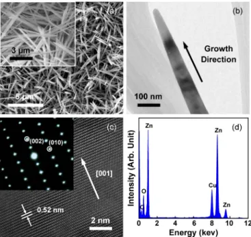
The top view of FE-SEM images of ZnO NWs is shown in Fig. 2(a). The deposition of ZnO NWs is observed to be highly uniform and dense. The sharp-tipped ZnO NWs have the average length of ∼5 μm and a diameter of ∼100 nm. Fig. 2(b) shows a typical TEM image of an individual ZnO NW peeled off from the Zn substrate and confirms that ZnO NWs are straight and uniform in shape. The HRTEM image shown in Fig. 2(c) represents a well-resolved lattice with a lattice spacing of 0.52 nm corresponding to the d spacing of the (001) crystal plane. Moreover, in the HRTEM images [inset in Fig. 2(c)], the growth direction of ZnO NWs is along the [001] direction which is the fastest growth direction for ZnO crystals. The corresponding SAED pattern reveals spot patterns, confirm-ing sconfirm-ingle-crystalline wurtzite structure elongated toward the
c-axis. In Fig. 2(d), EDS spectra show that the synthesized NWs
are composed of Zn and O. The small amount of Cu signals originated due to TEM copper grid.
Fig. 3(a) shows the XRD pattern of ZnO NWs on the Zn/glass substrate. The diffraction peaks indicated that ZnO NWs have hexagonal wurtzite structure. Furthermore, Fig. 3(b) shows PL spectra of ZnO NWs, indicating a strong UV peak and a broad yellow emission band. The UV peak centered at 378 nm and can be linked to the near-band-edge emission
Fig. 2. (a) Top-view FE-SEM images of ZnO NWs; inset shows the high mag-nification image. (b) TEM image. (c) HRTEM lattice image of an individual ZnO NW. The inset shows the corresponding SAED pattern. (d) EDS analysis.
Fig. 3. (a) X-ray diffraction pattern of ZnO NWs on Zn/glass substrate. (b) PL spectra measured at room temperature.
and free-exciton peak of ZnO [14]. The broad yellow bands of visible region are located at ∼560 nm and can be related to native defect levels within the bandgap, such as single and double ionized oxygen vacancies (deep level emission) [15]. The sufficient Zn2+from the Zn substrate and the slow release of OH− from H2O lead to oxygen deficiency and form the oxygen vacancy during the formation of ZnO NWs in the reaction chamber of SCCO2fluid process.
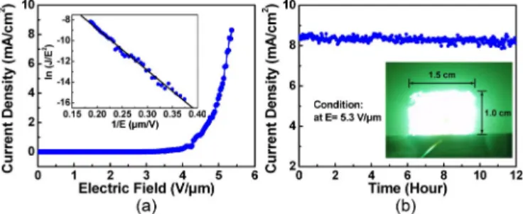
Fig. 4(a) shows the current–field (J−E) plot of ZnO emitters prepared on Zn/glass substrates. The turn-on electric field and threshold electric field of ZnO emitters were measured as 3.16 (at 10 μA/cm2) and 4.38 V/μm (at 1 mA/cm2), respec-tively. Furthermore, the FE curves can be modeled by the Fowler–Nordheim (F–N) equation expressed as [16]
J = (Aβ2E2/ϕ) exp(−Bϕ3/2/βE)
where J denotes the current density (in amperes per square meter), V is the applied voltage, E(V /d) is the applied field, d represents the distance between the anode electrode and top of emitters which is 100 μm, A = 1.56× 10⁻¹⁰(A eV/V2), B = 6.83× 10⁹(V/m eV3/2) [16], ϕ stands for the work function
YANG et al.: FE CHARACTERISTICS OF ZINC OXIDE NWs USING LOW-TEMPERATURE SCCO2FLUID METHOD 121
Fig. 4. (a) FE (J−E) plot of ZnO emitters. The inset shows corresponding F–N plots of the emission current. (b) Emission current stability at 5.3 V/μm within 12 h of testing. The inset shows FE micrograph of ZnO emitters.
of the emitter which is 5.4 eV [17] for ZnO, and β is the field-enhancement factor of ZnO emitters. β depends on the geometry of crystal structure, the density of the nanostruc-tures, and the work function. β is calculated from the slope of ln(J/E2) versus 1/E. The F–N plot of emission current is shown in the inset in Fig. 4(a). The curve exhibits linear behavior within the measured range, inferring consistency with the F–N theory. Fundamentally, the β of ZnO emitters was extracted as approximately 2142. FE properties of as-prepared ZnO NWs are not highly excellent, owing to structural defects (deep level emission). The structural defects of ZnO (i.e., oxygen vacancies, oxygen interstitials, zinc vacancies, and zinc interstitials) produce potential wells that can trap and impede the free movement of carriers, which will degrade the device performance [18], [19]. Current stability is a key issue for FE-based display devices. Fig. 4(b) shows the emission current stability within 12 h of testing. No obvious degradation of emission current density was observed; the emission current fluctuation was less than 8% at 5.3 V/μm in 12 h, and the mean emission current was about 8.3 mA/cm2. The inset in Fig. 4(b) shows the image of electron emission of ZnO emitters at an applied electric field of around 5.3 V/μm. It can be seen that the whole surface emission on the fluorescent screen is homogeneous. The results indicate that ZnO emitters prepared by low-temperature SCCO2 fluid method show the advanced FE characteristics and they are a promising candidate for FEDs on a variety of substrates.
IV. CONCLUSION
ZnO NWs were grown on Zn/glass substrates by a low-temperature SCCO2fluid method at 40◦C. ZnO NWs exhibit the average length of ∼5 μm and a diameter of ∼100 nm and represented single-crystalline wurtzite structure with an elongated c-axis. ZnO emitters demonstrated the supe-rior FE characteristics (i.e., the high current density, large field-enhancement factor (β) of 2142, low turn-on field of 3.16 V/μm, low threshold field of 4.38 V/μm, and low current fluctuation less than 8%), thus having potential applications in the flexible optoelectronics and FE devices.
REFERENCES
[1] Y. F. Zhukovskii, A. I. Popov, C. Balasubramanian, and S. Bellucci, “Structural and electronic properties of single-walled AlN nanotubes of different chiralities and sizes,” J. Phys., Condens. Matter, vol. 18, no. 33, pp. S2 045–S2 054, Aug. 2006.
[2] X. Qian, H. Liu, Y. Guo, Y. Song, and Y. Li, “Effect of aspect ratio on field emission properties of ZnO nanorod arrays,” Nanoscale Res. Lett., vol. 3, no. 8, pp. 303–307, Aug. 2008.
[3] K. C. Chen, C. F. Chen, J. H. Lee, T. L. Wu, C. L. Hwang, N. H. Tai, and M. C. Hsiao, “Low-temperature CVD growth of carbon nanotubes for field emission application,” Diamond Relat. Mater., vol. 16, no. 3, pp. 566–569, Mar. 2007.
[4] Y. Ryu, Y. Tak, and K. Yong, “Direct growth of core-shell SiC−SiO2
nanowires and field emission characteristics,” Nanotechnol., vol. 16, no. 7, pp. S370–S374, Apr. 2005.
[5] N. S. Ramgir, I. S. Mulla, K. Vijayamohanan, D. J. Late, A. B. Bhise, M. A. More, and D. S. Joag, “Ultralow threshold field emission from a single multipod structure of ZnO,” Appl. Phys. Lett., vol. 88, no. 4, pp. 042 107-1–042 107-3, Jan. 2006.
[6] J. J. Wu and S. C. Liu, “Low-temperature growth of well-aligned ZnO nanorods by chemical vapor deposition,” Adv. Mater., vol. 14, no. 3, pp. 215–218, Feb. 2002.
[7] Z. Zhang, J. Huang, H. He, S. Lin, H. Tang, H. Lu, and Z. Ye, “The influence of morphologies and doping of nanostructured ZnO on the field emission behaviors,” Solid State Electron., vol. 53, no. 6, pp. 578–583, Jun. 2009.
[8] C. W. Fang, J. M. Wu, L. T. Lee, Y. H. Hsien, S. C. Lo, and C. H. Chen, “ZnO:Al nanostructures synthesized on pre-deposited aluminum (Al)/Si template: Formation, photoluminescence and electron field emission,”
Thin Solid Films, vol. 517, no. 3, pp. 1268–1273, Jun. 2008.
[9] C. L. Hsu, S. J. Chang, H. C. Hung, Y. R. Lin, C. J. Huang, Y. K. Tseng, and I. C. Chen, “Well-aligned, vertically Al-doped ZnO nanowires synthesized on ZnO:Ga/glass templates,” J. Electrochem. Soc., vol. 152, no. 5, pp. G378–G381, Apr. 2005.
[10] C. T. Tsai, T. C. Chang, K. T. Kin, P. T. Liu, P. Y. Yang, C. F. Weng, and F. S. Huang, “A low temperature fabrication of HfO2films with
supercrit-ical CO2fluid treatment,” J. Appl. Phys., vol. 103, no. 7, pp. 074 108-1–
074 108-6, Apr. 2008.
[11] P. T. Liu, C. T. Tsai, T. C. Chang, K. T. Kin, P. L. Chang, C. M. Chen, and H. F. Cheng, “Activation of carbon nanotube emitters by using supercrit-ical carbon dioxide fluids with propyl alcohol,” Electrochem. Solid-State
Lett., vol. 9, no. 4, pp. G124–G126, Feb. 2006.
[12] M. Z. Yates, D. L. Apodaca, M. L. Campbell, E. R. Birnbaum, and T. M. McCleskey, “Micelle formation and surface interactions in super-critical CO2. Fundamental studies for the extraction of actinides from
contaminated surfaces,” Chem. Commun. (Cambridge), vol. 1, p. 25, 2001.
[13] M. Wang, S. J. Chua, H. Gao, J. S. Leib, and C. V. Thompson, “A study on morphology control of ZnO electrodeposited on Au surface,”
J. Electrochem. Soc., vol. 156, no. 11, pp. D517–D520, Oct. 2009.
[14] Z. K. Tang, G. K. L. Wong, P. Yu, M. Kawasaki, A. Ohtomo, H. Koinuma, and Y. Segawa, “Room-temperature ultraviolet laser emission from self-assembled ZnO microcrystallite thin films,” Appl. Phys. Lett., vol. 72, no. 25, pp. 3270–3272, Jul. 1998.
[15] K. Vanheusden, W. L. Warren, C. H. Seager, D. R. Tallant, J. A. Voigt, and B. E. Gnade, “Mechanisms behind green photoluminescence in ZnO phosphor powders,” J. Appl. Phys., vol. 79, no. 10, pp. 7983–7990, May 1996.
[16] R. H. Fowler and L. W. Nordheim, “Electron emission in intense electric fields,” Proc. R. Soc. Lond. A, Containing Papers Math. Phys. Character, vol. 119, no. 781, pp. 173–181, May 1928.
[17] Q. Zhao, X. Y. Xu, X. F. Song, X. Z. Zhang, D. P. Yu, C. P. Li, and L. Guo, “Enhanced field emission from ZnO nanorods via thermal anneal-ing in oxygen,” Appl. Phys. Lett., vol. 88, no. 3, pp. 033 102-1–033 102-3, Jan. 2006.
[18] H. Bong, W. H. Lee, D. Y. Lee, B. J. Kim, J. H. Cho, and K. Cho, “High-mobility low-temperature ZnO transistors with low-voltage operation,”
Appl. Phys. Lett., vol. 96, no. 19, p. 192 115, May 2010.
[19] P. Y. Yang, J. L. Wang, W. C. Tsai, S. J. Wang, J. C. Lin, I. C. Lee, C. T. Chang, and H. C. Cheng, “Oxygen annealing effect on ultravi-olet photoresponse of p-NiO-nanoflowers/n-ZnO-nanowires heterostruc-tures,” J. Nanosci. Nanotechnol., vol. 11, no. 7, pp. 5737–5743, Jul. 2011.