Comparison of MiM Performance with Various Electrodes
and Dieletric in Cu Dual Damascene of CMOS MS/
RF Technology
M. C. King,a,zC. F. Chang,b,
*
H. J. Lin,band Albert China aDepartment of Electronics Engineering, National Chiao Tung University, Hsinchu, Taiwan b
Taiwan Semiconductor Manufacturing Corporation, Tainan 741-44, Taiwan
In this paper, we have compared the performance of metal–insulator–metal 共MiM兲 capacitors for different bottom electrode materials including Cu, TaN, and Al in Cu–back-end-of-the-line共BEOL兲 process. A high-performance and low-defect-density MiM capacitor for mixed-signal and radio frequency 共MS/RF兲 technology based on a 130 nm complementary metal oxide semiconductor共CMOS兲 process was demonstrated. Q-factor can achieve ⬎100 for both Cu and Al at 2.4 GHz with 0.7 pF MiM capacitors. TaN showed a low Q-factor共⬍60兲 due to high resistivity. The process incorporates aluminum electrode into Cu– BEOL for MiM capacitor with a cost-effective process. The roughness of electro-dielectric interface by a thin aluminum electrode is critical for MiM performance due to field enhancement by roughness of a thin aluminum electrode. We have demonstrated a way to eliminate the roughness effect of thin Al and provide a MiM capacitor with high performance and low defect density. In particular, a method is demonstrated to achieve better matching, leakage, electrical breakdown, and temperature coefficient of capacitance performance for MiM capacitors.
© 2006 The Electrochemical Society. 关DOI: 10.1149/1.2354447兴 All rights reserved.
Manuscript submitted December 16, 2005; revised manuscript received May 24, 2006. Available electronically October 10, 2006.
High-quality passive elements integrated with logic have been the trend of mixed-signal and radio frequency共MS/RF兲 SoC. The on-chip integration of MiM inductors with logic process is popular for area, cost, and performance enhancement. For 0.18m technol-ogy and beyond, aluminum is used as the logic interconnects. While integrating MiM with the logic process, one interconnect layer is usually used as the bottom electrode plate of MiM capacitors. The thick Al interconnect共⬃4 k兲 offers a low resistivity and planar elec-trode which results in a high Q and low interface leakage. In the Cu back-end-of-line共BEOL兲 era, the use of Cu as the bottom electrode plate is the most cost-effective method because the Cu layer is also used for logic area without extra cost. Cu also has a very low resis-tivity and results in a high Q performance. Our results show that Cu can achieve Q⬇ 200 at 2.4 GHz with 0.7 pF MiM capacitor. How-ever, it has been reported that Cu roughness causes MiM reliability problems.1-3In addition, Cu can be used for small-area MiM but the performance is significantly degraded for larger area MiM capaci-tors. Cu roughness and Cu–chemical-mechanical polishing共CMP兲 m-scratch are two factors for the worse early breakdown of the bottom electrode plate. To develop highly reliable, high-Q, and high-yield MiM capacitors, we have compared different MiM bot-tom electrodes共Table I兲 and developed an optimized TaN/Al/TaN bottom electrode plate with thin Al thickness for mass production. The Q value can achieve 115 at 2.4 GHz with 0.7 pF MiM capacitor for the Al bottom electroplate. For the pure TaN bottom electroplate, the Q factor is significantly degraded by more than half due to high resistivity. For Al process, serious roughness is observed for the thin Al layer. To resolve the field enhancement due to roughness of the thin Al bottom electroplate, we have developed a method to opti-mize the process of aluminum deposition to fully resolve the effect. A high-Q, highly reliable, and capable of manufacturing MiM pro-cess in Cu-BEOL is realized.
MiM Capacitor Process
The process was based on the standard 0.13m complementary metal oxide semiconductor 共CMOS兲 technology provided by the foundry. After processing the 0.13m front-end-of-the-line 共FEOL兲 and Cu dual damascene process with an eight-level Cu interconnect, an Al MiM capacitor was inserted into the top two metal layers. The MiM structure is shown in Fig. 1. After the 7th metal layer was patterned after Cu-CMP, an etching-stop layer was deposited for
further processing. A thin aluminum layer was deposited and se-quentially followed by TaN deposition as the material for bottom plate. Plasma-enhanced chemical vapor deposition共PECVD兲 SiO2 or Si3N4was then deposited as the capacitor dielectric, followed by
TaN deposition as the top plate. Two masks were used to pattern the top plate and bottom plate. After oxide deposition, the via connec-tion is formed to connect the top plate, bottom plate, and logic area at the same time. The oxide topography due to the stacked MiM structure is polished by Cu-CMP while forming the top metal inter-connect. The resulting MiM capacitor has demonstrated high Q, high yield, and a wide process window for manufacturing. The current–voltage共I–V兲, capacitance–voltage 共C–V兲, and quality fac-tor共Q兲 were measured by HP4156, HP4284, and HP8510C, respec-tively.
MiM Capacitor Characterization
For rf application, the quality factor of MiM capacitors with different bottom electrodes is shown in Fig. 2. Copper can achieve a quality factor of ⬃200 and TaN/Al/TaN electrodes ⬃115 at 2.4 GHz with 0.7 pF. For the pure TaN bottom electrode plate, the
Q factor can only achieve⬃54 at 2.4 GHz due to higher resistivity.
The capacitance increases at high frequency due to the resonance of the parasitic inductor, which can be flattened out by a proper de-embedding procedure.
*Electrochemical Society Active Member.
z
E-mail: [email protected]
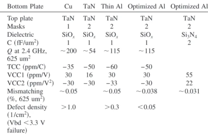
Table I. Comparison of MiM performance for different bottom electrode materials.
Bottom Plate Cu TaN Thin Al Optimized Al Optimized Al
Top plate TaN TaN TaN TaN TaN
Masks 1 2 2 2 2
Dielectric SiOx SiOx SiOx SiOx Si3N4
C共fF/um2兲 1 1 1 1 2 Q at 2.4 GHz, 625 um2 ⬃200 ⬃54 ⬃115 ⬃115 TCC共ppm/C兲 −35 −50 −60 −50 VCC1共ppm/V兲 30 16 30 30 55 VCC2共ppm/V2兲 −30 −30 −33 −30 22 Mismatching 共%, 625 um2兲 ⬃0.05 ⬃0.05 ⬃0.038 ⬃0.031 Defect density 共1/cm2兲, 共Vbd ⬍3.3 V failure兲 ⬎1.0 ⬎0.3 ⬍0.05
Journal of The Electrochemical Society, 153共12兲 G1032-G1034 共2006兲
0013-4651/2006/153共12兲/G1032/3/$20.00 © The Electrochemical Society G1032
) unless CC License in place (see abstract). ecsdl.org/site/terms_use
address. Redistribution subject to ECS terms of use (see 140.113.38.11
In addition to high Q, another important factor is the leakage current. This is especially important for high-density analog/rf inte-grated circuits共ICs兲 similar to the case of the dynamic random ac-cess memory共DRAM兲 capacitor.4,5In this work, we also optimized the MiM leakage current. Typical leakage共J–V兲 behavior of differ-ent bottom electrode materials is shown in Fig. 3. The asymmetrical leakage for applied voltage is due to the different roughness between top and bottom electrode plates. For positive applied voltage at the top electroplate, electrons are injected from the bottom plate to the top plate. The roughness of the bottom electro-plate is critical for creating sites with higher electric fields. Under low electric fields, the trap-assisted tunneling共TAT兲 of electrons from the electrode to trap states in the dielectric close to the electrode–dielectric interface dominate the capacitor leakage.6Nitride dielectric showed a higher MiM leakage dependence with the applied leakage compared with plasma-enhanced oxide共PEOX兲 dielectrics. This is caused by the intrinsic leakage characteristics of silicon nitride film. The leakage current is very low, in the range of⬍1 ⫻ 10−10A/cm2at 1.2 V for
optimized Al with SiOx. On the other way, the impact of asymmetric
leakage due to different top and bottom electrode plates is minor. The top electrode is deposited onto the dielectric material and there is no surface roughness issue. The top electrode plate is also de-signed to connect the top metal line through via array, and the re-sistance is much lower compared with the bottom electrode plate and has minimum impact on MiM performance.
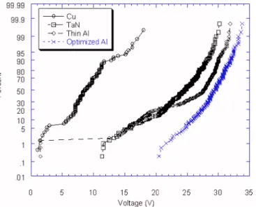
The comparison of MiM breakdown voltage共Vbd兲 performance is shown in Fig. 4, with 1,000,000m2MiM area for bottom
elec-trodes with TaN and Al and 640,000m2 for bottom electrodes with Cu. The Vbd cumulative failure of the Cu electrode plate is much worse than TaN and Al/TaN electrodes due to worse surface roughness and inevitable Cu-CMP dishing. For the small-area MiM capacitor, the Cu electrode is still an option but high defect density is a concern. For thin TaN/Al共⬍1.5 k兲/TaN electrode, the surface roughness is observed to be critical, which was not significant for conventional Al共⬎3 k兲/TiN bottom electrode plates beyond 0.18m technology. By optimizing the process temperature and other process conditions of Al deposition process, the degradation of MiM Vbd by surface roughness is significantly reduced.
The reflectivity of the Al/TaN electrode vs the waiting time of the Al process also demonstrated robust process after optimization, as shown in Fig. 5. Before the process is optimized, the reflectivity decreases significantly with process waiting time. For the optimized thin Al process, the dependence on the waiting time of the Al depo-sition process is negligible compared with the original one. This indicates that the optimized Al deposition has a stable surface rough-ness with a manufacturable process window.
Figure 1. Structure of integrated MiM capacitor with TaN/Al/TaN bottom electrode and TaN top electrode.
Figure 2. The quality factor of 25⫻ 25 m MIM capacitors. Cu has the highest quality factor with ⬃200 at 2.4 GHz. TaN/Al/TaN showed Q ⬃ 115, but TaN can achieve only 54 at 2.4 GHz.
Figure 3. Comparison of current vs voltage behavior for different bottom electrode materials.
Figure 4. MiM Vbd comparison with different bottom electrode plates. Wa-fers with optimized Al/TaN bottom electrodes showed the best breakdown voltage.
G1033
Journal of The Electrochemical Society, 153共12兲 G1032-G1034 共2006兲 G1033
) unless CC License in place (see abstract). ecsdl.org/site/terms_use
address. Redistribution subject to ECS terms of use (see 140.113.38.11
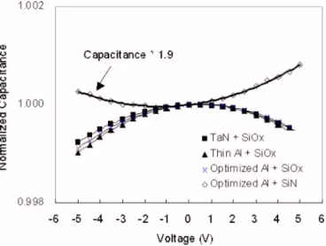
Linearity is a critical characteristic for capacitors. Figure 6 shows the normalized capacitance for four different bottom electrode plates vs temperature from 25 to 125 C. Cu demonstrates minimal first-order temperature coefficient of capacitance with less than 40 ppm/°C and ⬃30% reduction compared to TaN and TaN/Al/TaN. Figure 7 shows the normalized capacitance for three different bottom electrode plates and two dielectric materials vs the bias voltage from −5 to 5 V. TaN demonstrated much better first-order voltage coefficient of capacitance 共VCC1兲 compared with TaN/Al/TaN. The second-order voltage coefficient of capacitance 共VCC2兲 is comparable for different bottom electroplates. However, MiM dielectric with nitride has a positive VCC2共22 ppm/V2兲
com-pared to a negative VCC2共−30 ppm/V2兲 for SiO
xMiM dielectrics.
The negative second-order voltage coefficient of capacitance for SiOxdielectrics is due to the intrinsic leakage current while applying
voltage. The positive VCC2 of silicon nitride film is due to charge trapping in the nitride film.7
Conclusion
The incorporation of MiM capacitor into Cu-BEOL needs a dif-ferent approach compared with 0.18m technology. The adoption of process options depends on the intent of product design and MiM area. For high-Q and small MiM area product, Cu as a capacitor bottom plate is a suitable option but has a lower process yield. TaN-based MiM capacitor can achieve low leakage and linearity but a penalty of a low quality factor of⬃54 at 2.4 GHz due to high resistivity. A MiM capacitor with a thin Al bottom plate can also be achieved with optimized process condition. The Al-based MiM ca-pacitor can achieve Q⬎ 100 at 2.4 GHz with ⬃0.7 pF. The opti-mized process conditions can achieve a very low defect density suitable for manufacturing.
Acknowledgements
The authors would like to thank C. T. Lin, C. H. Chen, C. L. Chang, and C. C. Ku for their measurement and recommendations. National Chiao-Tung University assisted in meeting the publication costs of this article.
References
1. C. C. Lin, H. M. Hsu, Y. H. Chen, T. Shih, S. M. Jang, C. H. Yu, and M. S. Liang, in Proceedings of 2001 International Interconnect Technology Conference, pp. 113–115, June 2001.
2. C. H. Ng, K. W. Chew, J. X. Li, T. T. Tjoa, L. N. Goh, and S. F. Chu, Tech. Dig. – Int. Electron Device Meet., pp. 241–244, Dec 2002.
3. Y. L. Tu, H. L. Lin, L. L. Chao, D. Wu, C. S. Tsai, C. Wang, C. F. Huang, C. H. Lin, and J. Sun, Digest of Technical Papers, 2003 Symposium on VLSI Technology, pp. 79–80, June 2003.
4. H. Hu, S. J. Ding, H. F. Lim, C. Zhu, M. F. Li, S. J. Kim, X. F. Yu, J. H. Chen, Y. F. Yong, B. J. Cho, D. S. H. Chan, S. C. Rustagi, M. B. Yu, C. H. Tung, A. Du, D. My, P. D. Fu, A. Chin, and D. L. Kwong, Tech. Dig. - Int. Electron Devices Meet., 15.6.1–15.64, 2003.
5. C. Zhu, H. Hu, X. Yu, A. Chin, M. F. Li, and D. L. Kwong, Tech. Dig. - Int. Electron Devices Meet., 36.5.1–36.54, 2003.
6. T. Remmel, R. Ramprasad, and J. Walls, in Proceedings of 41st Annual Interna-tional Reliability Physics Symposium, pp. 277–281, April 20, 2003.
7. A. Yin, J. White, A. Karroy, and C. Hu, in Proceedings of Solid-State and Inte-grated Circuit Technology, 5th International Conference, pp. 131–134共1998兲.
Figure 5. Normalized reflectivity vs Al-deposition waiting time to show the relative surface roughness effect. Conventional thin Al has a decreasing re-flectivity with longer Al-chamber waiting time. This means the surface roughness is unstable for conventional Al process condition.
Figure 6. Comparison of temperature linearity on MiM capacitors. Cu bot-tom electroplate has the smallest TCC1 with −35 ppm/°C.
Figure 7. Comparison of voltage linearity on MiM capacitors. Nitride di-electric showed a positive VCC2 compared with a negative VCC2 of SiOx.
G1034 Journal of The Electrochemical Society, 153共12兲 G1032-G1034 共2006兲
G1034
) unless CC License in place (see abstract). ecsdl.org/site/terms_use
address. Redistribution subject to ECS terms of use (see 140.113.38.11