14.2
Auger Recombination Enhanced Hot Carrier Degradation in nMOSFETs
with Positive Substrate Bias
L.P. Chiang, C.W. Tsai, T. Wang
Department of Electronics Engineering, National Chiao-Tung University, Taiwan U.C. Liu, M.C. Wang and L.C. Hsia
Technology and Process Development Division, UMC, Hsin-Chu, Taiwan
Abstract
Enhanced hot carrier degradation is observed in DTMOS-like operation mode. This phenomenon is attributed to Auger recombination assisted hot electron process. Measured hot electron gate current and light emission spectrum in nMOSFETs provide evidence that the high-energy tail of channel electrons is increased by the application of a positive substrate bias. As opposed to conventional hot carrier degradation, the Auger enhanced degradation exhibits positive temperature dependence and is more significant at low drain bias.
Introduction
In certain analog and digital circuits, positive substrate bias is applied in nMOSFETs to achieve better performance. For example, improved transistor matching properties and lower flicker noise in analog MOSFETs [1,2] and higher Ion /Io ff ratio in DTMOS [3,4] were reported. The applied substrate bias is sometimes as large as 0.7V [5] or even above [6,7]. The reliability issue of MOSFETs in such bias condition is rarely studied. In this paper, we will report enhanced hot carrier degradation in DTMOS-like operation. The observed degradation cannot be simply explained by conventional channel hot electron theory. Instead, an Auger recombination assisted hot electron energy gain process is proposed. In our model (Fig. l), holes are injected from positively biased substrate to the channel, which provide for recombination with electrons in the inversion region and give the excess energy to other electrons. The energetic electrons arising from Auger process are then accelerated by channel electric field, thus resulting in a larger hot electron tail than in the standard MOSFET operation condition.
Device Characterization
A four-terminal nMOSFET is used in this work. The device ha: a gate length of 0.25pm, a gate oxide thickness about 50A and a gate width of 100pm. Maximum Ib stress around Vg=O.5Vd is performed in DTMOS-like mode (Vb>O) and in the standard mode (Vb=O). Drain current in the triode region is measured to monitor degradation. Temperature and drain bias dependence of the Auger enhanced degradation is characterized.
Results and Discussion
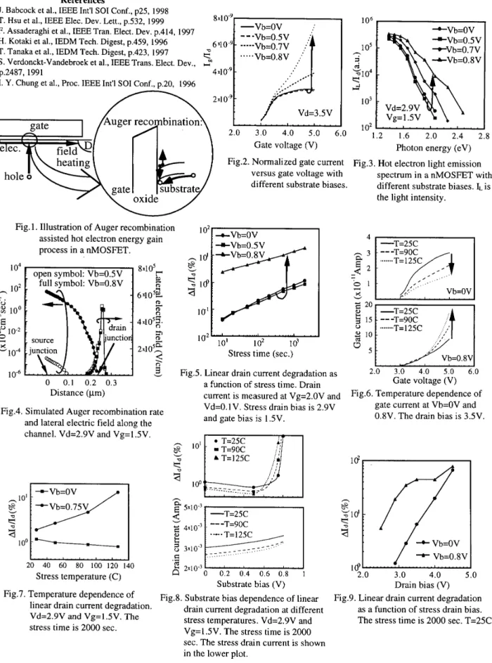
( a ) Auger effect enhanced hot electron tail Hot electron gate current in the standard mode and in DTMOS mode is shown in Fig. 2. The gate current first decreases and then increases with Vb. Hot electron luminescence and emission spectrum are measured to analyze the hot electron distribution (Fig. 3). The light intensity is normalized to the drain current to compensate for the different carrier flux in the channel. Similarly, the emission
132
. 0-7803-6305-4/00/$10.00 0 2000 IEEEspectrum shows a turn-around feature as Vb increases from
ov
to 0.8v. The reduction of Ig/Id and IL/Id at Vb=o.5V is due to a smaller lateral electric field. At vb=o.8v, although the lateral field continues to decrease, the Auger recombination rate increases considerably, thus leading to larger Ig/Id and IL/Id. Fig. 4 shows the simulation result of Auger recombination rate and electric field in the channel. Note that hole injection is restricted to the low field region near the source. To further demonstrate the Auger effect on device reliability, the linear drain current degradation at different Vb is measured (Fig. 5). The drain current degradation is increased by an order of magnitude when Vb is from OV to 0 . W .(b) Temperature accelerated degradation
The temperature effect on the Auger enhanced degradation is investigated. We compare the temperature dependence of hot electron gate current in the standard mode and in DTMOS mode (Fig. 6 ) . The gate current at Vb=OV has negative temperature dependence due to increased phonon scattering at a higher temperature. This result is consistent with conventional hot electron theory. However, the gate current in DTMOS mode shows reversed Ig-temperature dependence. The reason is that hole injection and Auger recombination rate are enhanced at an elevated temperature. To our knowledge, this is the first time to observe positive temperature dependence of hot electron gate current.
The temperature effect on drain current degradation is shown in Fig. 7. Temperature accelerated degradation is noticed in DTMOS mode. The degradation is enhanced by eight times from T=25C to T=125C. This point is particularly important to device reliability since today's high performance components are required to operate in such temperature range. The substrate bias dependence of drain current degradation is shown in Fig. 8. The measured result shows opposite temperature dependence in the low Vb region and in the high Vb region. The critical Vb for the onset of the Auger enhanced degradation becomes smaller as temperature increases.
( c ) Drain bias dependence of degradation
The dependence of the Auger enhanced drain current degradation on stress drain bias is evaluated (Fig. 9). At a relatively large drain bias, the dominant electron energy gain mechanism is field heating. The degradation in DTMOS mode and in the standard mode is therefore about the same. As drain bias reduces, electrons by field heating solely do not have sufficient energy for interface trap creation. The combined Auger recombination and channel field heating process can increase hot electron energy above the threshold for trap creation. Consequently, the Auger enhanced degradation appears to be more significant at low drain voltage in Fig. 9.
References
[I] J. Babcock et al., IEEE Int'l SO1 Conf., p25, 1998 [2] T. Hsu et al., IEEE Elec. Dev. Lett., p.552, 1999 [3] F. Assaderaghi et al., IEEE Tran. Elect. Dev. p.414, 1997
[4] H. Kotaki et al., IEDM Tech. Digest, p.459, 1996 6~10.~: ,
---vJ
Vb=O.8V : [5] T. Tanaka et al., IEDM Tech. Digest, p.423, 1997[6] S. Verdonckt-Vandebroek et al., IEEE Trans. Elect. Dev.,
Auger reco bination:
Gate voltage (V) Fig.2. Normalized gate current
versus gate voltage with different substrate biases.
V e l e c . '
field
8.10.';
-Vb=OV ---Vb=O.SV%
.
.
' ,*.a p.2487, 1991 4 ~ 1 0 . ~ - . . . .*[7] I. Y. Chung et al., Proc. IEEE Int'l SO1 Conf., p.20, 1996
:,.-
. ..
2.10.~ - Vd=3.5VI
,
-
2.0 3.0 4.0 5.0 6.0substrate
oxide
1
&Vb=OVgate
heating
hole
ogate
Fig. 1. Illustration of Auger recombination
I
assisted hot electron energy gainprocess in a nh4OSFET.
0 0.1 0.2 0.3 Distance (pm)
Fig.4. Simulated Auger recombination rate and lateral electric field along the channel. Vd=2.9V and Vg=l S V .
10211bl . l b 2 ' ""I> . - . I Stress time (sec.)
Fig.5. Linear drain current degradation as a function of stress time. Drain current is measured at Vg=2.OV and Vd=O.lV. Stress drain bias is 2.9V and gate bias is 1 SV.
1 0 6 1
os
%io4 1o3
1o2
9 m ?r,
U 1.2 1.6 2.0 2.4 2.8 Photon energy (eV) spectrum in a nMOSFET with different substrate biases.4.
is the light intensity.Fig.3. Hot electron light emission
I
0 3 0 4 0 S O 6 0
Gate voltage (V) Fig.6. Temperature dependence of
gate current at Vb=OV and 0.8V. The drain bias is 3.547.
l ' 2 8 # 8 l 20 40 60 80 100 120 140 3.0 4.0 5.0 Drain bias (V) E 2x10'3
-
a
o 0.2 0.4 0.6 0.8 I Substrate bias (V) Stress temperature (C)Fig.7. dependence of Fig.8. Substrate bias dependence of linear Fig.9. Linear drain current degradation as a function of stress drain bias. The stress time is 2000 sec. T=25C. linear drain current degradation.
Vd=2.9V and Vg=l.W. The stress time is 2000 sec.
drain current degradation at different stress temperatures. Vd=2.9V and Vg=lSV. The stress time is 2000 sec. The stress drain current is shown in the lower plot.