國立交通大學
資訊科學與工程研究所
碩 士 論 文
軟體化延遲鎖定迴路之研究與實作
The Study of Software-defined Delay-locked Loop
and Its Implementation
研 究 生:洪崇文
指導教授:許騰尹 教授
軟 體 化 延 遲 鎖 定 迴 路 之 研 究 與 實 作
The Study of Software-defined Delay-locked Loop and Its
Implementation
研 究 生:洪崇文 Student:Chung-Wen Hong
指導教授:許騰尹 Advisor:Terng-Yin Hsu
國 立 交 通 大 學
資 訊 科 學 與 工 程 研 究 所
碩 士 論 文
A ThesisSubmitted to Institute of Computer Science and Engineering College of Computer Science
National Chiao Tung University in partial Fulfillment of the Requirements
for the Degree of Master
in
Computer Science July 2011
Hsinchu, Taiwan, Republic of China
摘要
延遲鎖定迴路具有消除時脈歪斜的功能,目前已被廣泛應用於各種系統的同 步電路,用以提供一個穩定的系統時脈。本篇論文提出了可使用軟體來控制並達 到相位鎖定的軟體定義之延遲鎖定迴路平台(SDDLL)。此平台同時具有消除時脈 歪斜、多相位的時脈輸出以及工作週期校正等功能,以 WISHBONE bus 結合了 OPENRISC 的 or1200 CPU 以及全數位式延遲鎖定迴路的數個 IP。CPU 可以進行軟 體指令的執行與運算,在平台的應用以及規格改變時,只需要修改軟體便可符合 規格,避免掉重新設計硬體的流程,減少時間及金錢的消耗,提升了重複利用度 以及彈性。此平台所有的矽智財是建立在 TSMC65nm GP 1P6M 製程下,軟體部分 則是使用 gcc 以及 GNU toolchain 來實作。
Abstract
Delay-locked loop can do clock deskew, and it is widely applied to the synchronous circuits on various hardware systems nowadays. It can provide a stable system clock. In this paper, a software-controllable and phase-lockable platform of software-defined delay-locked loop(SDDLL) is proposed. This platform can do clock deskew, multiphase output clock and duty cycle calibration. It is combined of OPENRISC or1200 CPU and several intellectual properties in all-digital delay-locked loop. CPU can execute the software instructions and do many operations. When the application or specification of the platform is changed, it only needs to modify the software and the platform still meet the new specification. The DLL can avoid the procedure of the hardware redesign, so the verification of locking strategy can be faster due to the reusability and the flexibility of software. All of the silicon IPs of the platform are fabricated in TSMC65nm GP 1P6M process, And the software are implemented by gcc and GNU toolchain.
Acknowledgement
要感謝的人非常多,首先我想感謝指導教授許騰尹老師,老師總是在各方面 給我適當的建議,不只是研究上,連做事情的方式上也總能點出我的缺點,因此 才有這篇論文的產生,十分感謝老師,我學到了不少東西,再來是 ISIP 的博士 班學長們,學長們也在各方面給了我莫大的幫助,以及實驗室的學長姐、同學與 學弟妹們,謝謝大家給了我很多的鼓勵,最後要感謝父母兄長及朋友,沒有他們, 便不會有今日的我了,在此致上我最真摯的謝意給以上所有人。 洪崇文 謹誌 民國一百年七月Table of Contents
摘要... i Abstract ... ii Acknowledgement ... iii Table of Contents ... iv List of Figures ... viList of Tables ... vii
Chapter 1 Introduction ... 1 1.1. Thesis Motivation ... 1 1.2. Thesis Contribution ... 1 1.3. Thesis Organization ... 2 Chapter 2 Overview of SDDLL ... 3 2.1. Basic Concept ... 3 2.2. Locking Issue ... 5 2.2.1. False-locking ... 5 2.2.2. Harmonic-locking ... 6 2.3. Locking Strategy ... 8 2.3.1. TDC ... 8
2.3.2. Pulse Amplifier with One Pulse Lock ... 9
Chapter 3 The Architecture of The Proposed SDDLL ... 10
3.1. Basic Concept of SDDLL ... 10
3.2. The Architecture of SDDLL ... 11
3.2.1. CPU ... 12
3.2.2. BUS ... 13
3.2.3. Semi Asynchronous Clock Access (SACA) ... 13
3.3. The Hardware Architecture of DLL ... 14
3.3.1 Multiphase DCDL ... 16
3.3.2. Coarse Delay Line... 18
3.3.3. Fine Delay Line... 18
3.3.4. Duty Cycle Corrector ... 20
3.4. The Hardware Specification of SDDLL ... 22
Chapter 4 The Control Strategy of The Proposed SDDLL ... 23
4.1. Control Strategy ... 23
4.2. Software Design Issues ... 26
4.2.1. Redundancy Cycle ... 26
4.2.2. Software Environment ... 29
Chapter 5 Conclusion and Future Work ... 39 Reference ... 40
List of Figures
Fig. 1. Basic block diagram of ADDLL. ... 4
Fig. 2. The delay adjustment of DLL. ... 5
Fig. 3. The timing diagram of false-locking when the input clock period is 5ns. ... 6
Fig. 4. The timing diagram of Harmonic-locking when the input clock period is 5ns. . 7
Fig. 5. The architecture of TDC. ... 8
Fig. 6. The architecture of Pulse Amplifier with One Pulse Lock. ... 9
Fig. 3.1. The basic concept of SDDLL. ... 11
Fig. 3.2. The architecture and data flow of SDDLL platform. ... 12
Fig. 3.3. The overview of OPENRISC Or1200. ... 13
Fig. 3.4. An example of SACA. ... 14
Fig. 3.5. The architecture and the data flow of DLL. ... 15
Fig. 3.6. The waveform of reference clock and extended pulse. ... 15
Fig. 3.7. The architecture of 8-stage Multiphase DCDL. ... 16
Fig. 3.8. The waveform of 8-stage Multiphase DCDL. ... 17
Fig. 3.9. The architecture of fine delay line. ... 19
Fig. 3.10. The transistor-level representation for AOI21D4. ... 20
Fig. 3.11. The architecture of Duty Cycle Corrector... 21
Fig. 3.12. The architecture of Duty Cycle Corrector Unit. ... 21
Fig. 3.13. The example waveform of duty cycle calibration. ... 22
Fig. 4.1. The coarse and fine part of control signal. ... 23
Fig. 4.2. An example state diagram of the coarse-fine tuning. ... 24
Fig. 4.3. The state diagram of SDDLL’s control strategy. ... 25
Fig. 4.5. The flow of Prune-and-Search. ... 26
Fig. 4.6. The tuning without redundancy cycles. ... 27
Fig. 4.7. The tuning with redundancy cycles. ... 27
Fig. 4.8. The software-executing flow without code rearrangement. ... 28
Fig. 4.9. The software-executing flow with code rearrangement. ... 29
Fig. 4.10. The waveforms of simulation result. ... 32
Fig. 4.11. The waveforms of simulation result with an enabled 8-order Moving- average filter... 34
Fig.4.12. The pre-sim of 8-stage Digital-controlled Delay Line. ... 36
List of Tables
Table 1. The specification of one delay line ... 18
Table 2. Hardware Specification ... 22
Table 3. Software environment ... 30
Chapter 1
Introduction
1.1. Thesis Motivation
Delay-locked loop has been widely used for synchronous circuits between the system chips. There are several kinds of delay-locked loops, such as Analog DLL, Digital DLL (DDLL), All-digital DLL (ADDLL). ADDLL means that all of the components are digital. In general, all-digital approach has higher portability and shorter design cycle and fast-locking property. But when the application or control strategy is changed, DLL have to do hardware redesign. It spends a lot of time for simulation, synthesis, layout and verification for IC design standard flow. Therefore, the Software-defined Delay-locked Loop (SDDLL) is proposed. DLL can use software to control the delay-locked loop. The platform of SDDLL integrated with CPU and all IPs for delay-locked loop just like an embedded system. Software has flexibility and the time for development is shorter. Hence, SDDLL has flexibility and reusability. And the redesign cost can be alleviated.
1.2. Thesis Contribution
The proposed platform of SDDLL can control the delay locked loop via the software. It is just like an embedded system hardware-software codesign. The platform can do clock-deskewing, multiphase output clock and duty cycle calibration. The software can be optimized to reduce the redundancy cycles for phase tracking procedure. When the application or the specification is changed, DLL can modify the software to fit the new condition.
1.3. Thesis Organization
Section 2 shows the overview of conventional ADDLL and SDDLL. Section 3 illustrates the architecture of the proposed SDDLL. Section 4 illustrates the control strategy of the proposed SDDLL and the simulation result. Section 5 presents conclusions and future works.
Chapter 2
Overview of SDDLL
The characteristics of the proposed SDDLL are software controllability and programmability. SDDLL combines the CPU and the silicon IPs of the delay-locked loop, so the hardware and software can work in coordination with each other. All of the components will be discussed as follows.
2.1.
Basic Concept
There are several types of delay-locked loop. On the whole, all-digital approach has the fast-locking feature and higher tolerance to process variation and the supply voltage, but its skew and jitter are more serious relatively. However, for SoC implementation, all-digital approach is more suitable due to the compatibility for integration system and the insensitivity to supply noise. So All-digital Delay-locked Loop(ADDLL) is chosen as the basic DLL IPs for the platform of the proposed SDDLL.
Delay-locked loop can generate an output clock whose phase is related to the reference clock via a delay chain. Therefore, the delay time should be integral multiples of reference clock’s period when the DLL is locking.
N n n T n Tdelay * ref, 1, (1) delay
T is the total delay time of the delay chain when the phase is locking, and Tref is the clock period of the reference clock.
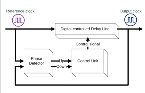
The conventional All-digital Delay-locked Loop contained several components, such as Phase Detector (PD), Digital-controlled Delay Line (DCDL) and the control unit for DCDL.
Digital-controlled Delay Line Control Unit Phase Detector Up Control signal Down Output clock Reference clock
Fig. 1. Basic block diagram of ADDLL.
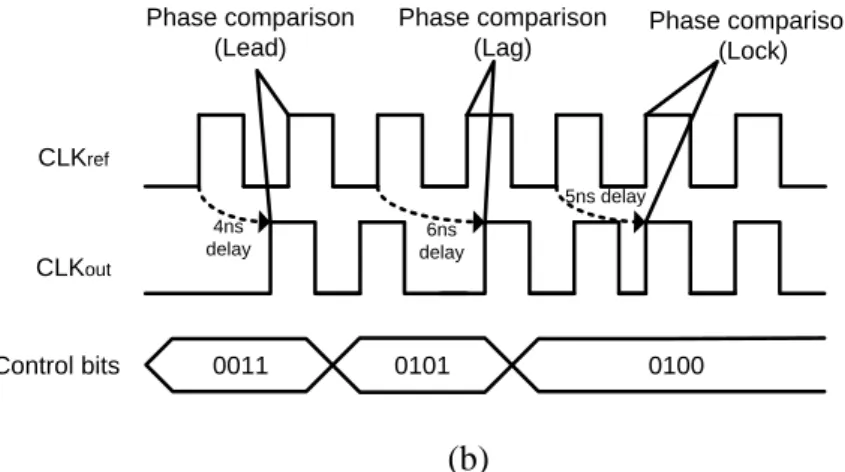
The architecture of ADDLL is shown in Fig.1. The Phase Detector compares the phase relation between the reference and output clock. The control unit can change the digital signal to adjust the delay time of DCDL according to the output of Phase Detector. If the output clock is leading the reference clock, the control unit can extend the delay time of DCDL. On the contrary, if the output clock is lagging the reference clock, the control unit can shorten the delay time of DCDL. Fig. 2 shows that an illustration of phase tracking for the 4-bit DCDL. Assume that the intrinsic delay of DCDL is 1ns, and the After appropriate phase tracking for the delay time of DCDL, the DLL should be locking.
Control Signal Delay Time 0000 1ns 0001 2ns 0010 3ns 0011 4ns 1111 16ns (a)
CLKref CLKout Control bits 0011 0101 0100 4ns delay Phase comparison (Lead) Phase comparison (Lag) Phase comparison (Lock) 6ns delay 5ns delay (b)
Fig. 2. The delay adjustment of DLL. (a)The example 4-bit delay line.
(b)The timing diagram of phase tracking when the input clock period is 5ns.
In consideration of the actual conditions, phase-tracking has some tough questions to solve. Because of the influence of input jitter and intrinsic jitter of DCDL and the dead zone of PD, it is more difficult to achieve lock state. This design should consider these unideal effects. If the DLL is in the locking state, there is still a few phase error. In general, the amount of phase error is associated with the resolution of DCDL.
2.2. Locking Issue
2.2.1.
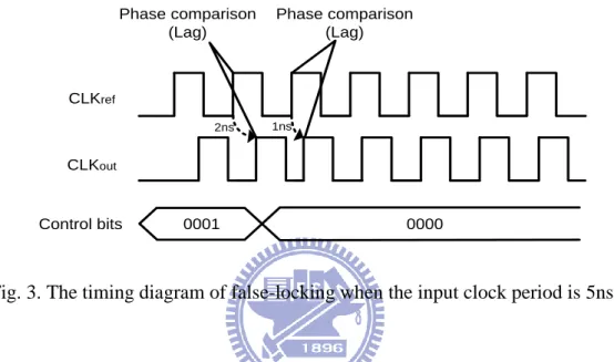
False-lockingFalse-locking is also called Stuck-locking. False-locking will cause the DLL could not achieve the phase-locking state permanently. If the initial delay of DCDL is shorter than half of input clock period, then false-locking occurs.
Ti n i t *Tr e f
2 1
(2)
init
T is the initial delay of DCDL, Tref is the period of reference clock. If the inequality (2) is true, the false-locking occurs. Fig. 3 shows the result of false-locking.
CLKref CLKout Control bits 0001 0000 Phase comparison (Lag) Phase comparison (Lag) 2ns 1ns
Fig. 3. The timing diagram of false-locking when the input clock period is 5ns.
Because the initial delay is shorter than half of reference clock, the phase of output clock is more near the original one. Therefore, PD determines that the output clock is lagging. The delay should be shorter. At last, the control signal should be zero, that is, the delay will be the shortest. However, DLL still could not lock because it is impossible for DCDL to be zero delay. Therefore, the clock-deskew function of DLL is also meaningless. The DLL design have to avoid the occurrence of the false-locking.
2.2.2.
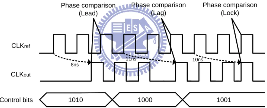
Harmonic-lockingHarmonic-locking actually can successfully lock the phase in the end. It means that the delay time of DCDL is larger than one reference cycle. Although DLL is still able to lock, the longer delay path will increase the intrinsic jitter of DCDL. Furthermore, if the DLL has multiphase applications, then the harmonic-locking is not allowed. The reason is that DLL needs to divide one reference cycle delay into multi-part to generate the multiphase output
clock.
The result of Harmonic-locking is as follows.
N n n T n Tdelay * ref, 2, (3) delay
T is the total delay time of the delay chain when the phase is locking, and Tref is the clock period of the reference clock. Moreover, The condition that brings about
Harmonic-locking is as follows. Tinit *Tr e f 2 3 (4) init
T is the initial delay of DCDL. When the inequality (4) is true, the delay time will approach two or more reference cycles. The timing diagram is shown in Fig 4.
CLKref CLKout Control bits 1010 1000 Phase comparison (Lead) Phase comparison (Lag) 8ns Phase comparison (Lock) 1001 10ns 11ns
Fig. 4. The timing diagram of Harmonic-locking when the input clock period is 5ns.
The final delay time in Fig. 4 is two reference clock cycles. It can notice that the DLL also need more than two cycles to adjust the delay time of DCDL because it must wait about two reference clock cycles to detect the real delayed phase for each tuning. Apart from this, Harmonic-locking is not that big problem when DLL does not provide multiphase applications. If the false-tracking and harmonic-tracking should be avoided, the DLL should fulfill the following condition.
Tref Tinit *Tref
2 3 * 2 1 (5)
2.3. Locking Strategy
The locking strategy of Digital DLL can be divided into several categories. The most conventional method is the sequential search algorithm, i.e., the shift register-controlled DLL and the counter-controlled DLL. But the lock-in time of DLL increases exponentially with the number of control bits. The second one is the successive-approximation register-controlled DLL (SARDLL). The strategy of SARDLL is like the binary search algorithm, so its lock-in time can be shorter. The last one is Time-to-digital Converter (TDC) scheme. TDC can roughly estimate the input clock period and use a digital output to represent it. According to the digital output, The DLL can set up the delay of DCDL. TDC can achieve the shortest lock-in time at the cost of area and power. In this work, the SDDLL will adopt the above methods.
2.3.1.
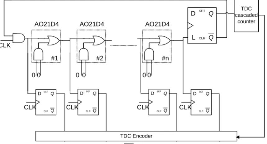
TDCThe architecture of TDC is shown in Fig. 5. TDC can measure an input pulse and give a corresponding digital output via a cascaded counter and D-type flip-flops.
AO21D4 #1 AO21D4 #2 AO21D4 #n 0 0 0 0 0 0 Q Q SET CLR D L TDC cascaded counter CLK Q Q SET CLR D Q Q SET CLR D Q Q SET CLR D Q Q SET CLR D TDC Encoder CLK CLK CLK CLK Quantization output
Fig. 5. The architecture of TDC.
DCDL is appropriate. The initial delay time of DCDL can approach one reference clock period quickly, so DLL can achieve faster phase-locking. Moreover, the locking issues will not take place due to the appropriate initial delay. TDC is used to accelerate phase-locking and solve the conventional locking issues.
2.3.2.
Pulse Amplifier with One Pulse LockTDC has its minimum measurable pulse width because of the setup time of D-type flip-flops and a little gate delay. If the input pulse is too short, the TDC cannot detect the existence of input pulse. Therefore, this design adopt the Pulse Amplifier to extend the narrow pulse to avoid the input pulse violation of TDC. Fig. 6 shows the architecture of Pulse Amplifier. Delay Path RB D Q RB D Q Error_set INPUT_PULSE 1 1 OUTPUT_PULSE
Fig. 6. The architecture of Pulse Amplifier with One Pulse Lock.
If the input pulse is too narrow, the Pulse Amplifier can extend the length of input pulse to the total delay path and output the new pulse. It solves the input violation problem of TDC. The Pulse Amplifier can also filter the other pulses after the first pulse via the control of Error_set, that is, the function of one pulse lock.
Chapter 3
The Architecture of The Proposed SDDLL
SDDLL combines the Or1200 CPU and DLL IPs via the WISHBONE bus. Resolution, range of operating frequency and lock-in time are important performance for DLL, so they should be take into account in the DLL design.
It is a big challenge for SDDLL to keep the above performance factor with the communication of hardware and software. The proposed SDDLL supply multiphase output clock and duty cycle calibration, so a multiphase DCDL and duty cycle correctors are adopted in this work.
The organization of this section is as follow. Section 3.1 introduce the basic concept of SDDLL. Section 3.2 shows the architecture of the proposed SDDLL and the communication interface of hardware and software. Section 3.3 shows the detailed silicon IPs of the hardware part of DLL.
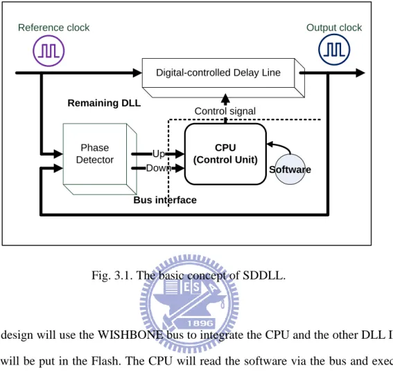
3.1. Basic Concept of SDDLL
In the conventional ADDLL, the control unit implements the control strategy and adjusts the control signal to change the delay time of DCDL. The main idea of SDDLL is that replacing the control unit by CPU and software. Let CPU execute the control strategy and tune the delay chain because the software has more flexibility and portability. SDDLL is just like an embedded hardware and software codesign. There are several CPUs in many systems nowadays. If some of them are idle, DLL can also steal the CPU to do phase-tracking for DLL. The control strategy can be modified for different usages easily, but we should be careful for
the software code writing.
Digital-controlled Delay Line
Phase Detector Up Control signal Down Output clock Reference clock CPU (Control Unit) Bus interface Remaining DLL Software
Fig. 3.1. The basic concept of SDDLL.
This design will use the WISHBONE bus to integrate the CPU and the other DLL IP. The software will be put in the Flash. The CPU will read the software via the bus and execute it, and the CPU can also exchange data with DLL via the bus. Therefore, the CPU can control the delay line in the DLL block.
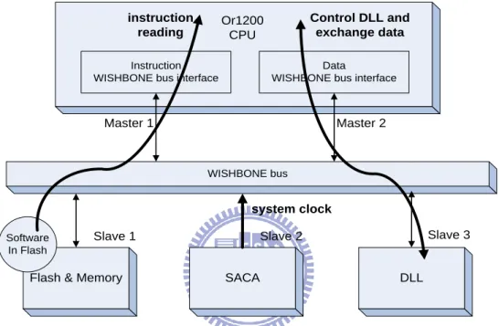
3.2. The Architecture of SDDLL
The or1200 CPU provides the bus interface for WISHBONE bus. This work selects compatible WISHBONE bus to integrate the CPU and all the silicon IPs. The WISHBONE bus is a master-slave interface and asynchronous access mechanism. The or1200 CPU is the master, and it can make a request to the slave for read or write. The architecture is shown in Fig. 3.2.
The software is compiled by GNU toolchain first, and the compiled machine code is stored into the read-only flash. After the system is reset, CPU will access the instructions from
the flash and execute it. CPU can do memory access for data read and write to complete all of the instructions. CPU can also communicate with the DLL via the bus, so they can exchange the information just like TDC output, phase state and digital control signal. SACA is in charge of the system clock generator. The system clock is transferred to all of the blocks via the WISHBONE bus.
WISHBONE bus Instruction
WISHBONE bus interface
Data
WISHBONE bus interface
Master 1 Master 2
DLL SACA
Flash & Memory
Slave 1 Slave 2 Slave 3
Or1200 CPU Software In Flash system clock instruction reading Control DLL and exchange data
Fig. 3.2. The architecture and data flow of SDDLL platform.
3.2.1.
CPUThe control unit is replaced with the or1200 CPU. The or1200 CPU is a free open source, released by OpenCores. The or1200 is 32-bit scalar RISC structure with the Harvard architecture, so Or1200 do instruction and data access separately. The used Or1200 is an uni-core CPU.
In this work, This design enables a 1K instruction cache in order to reducing the number of instruction access. In general, one bus access needs three system cycles to handle it. But if there is a cache hit, the instruction access only spends one system cycle. Otherwise, cache miss needs the miss penalty to recover the missing instruction. Or1200 will fetch the after
four instructions for miss penalty, so it needs twelve system cycles.
The data cache is disabled because the repeated data access for the same address is rare. And the address is not continuous, so enabling the data cache is not worth.
The gate count of CPU with 1KB instruction cache is about 150K in TSMC 65nm process. The reason why choosing Or1200 is that it is an open source and has implemented in various commercial systems.
Instruction wishbone bus interface
Data
wishbone bus interface Instruction cache (1KB enabled) Instruction MMU (disabled) Data cache (disabled) Data MMU (disabled) Programmable Interrupt Controller
Tick Timer Power
Management
Or1200 CPU
Fig. 3.3. The overview of OPENRISC Or1200.
3.2.2.
BUSOr1200 provides WISHBONE bus interface. The WISHBONE bus has high compatibility because it is an asynchronous bus. That is, it choose the hand-shaking mechanism for the communication. The master make a request with the access address. The bus will transform the request to the related slave. The slave will give an ack back to master, and then the data transition starts.
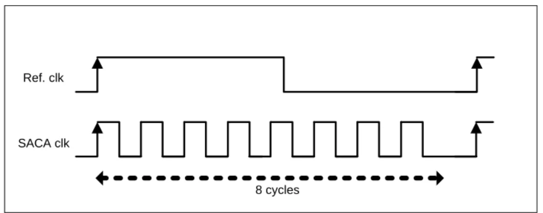
3.2.3.
Semi Asynchronous Clock Access (SACA)the system clock via the WISHBONE bus. SACA can multiply the clock frequency with a digital control signal. SACA can apply better performance in circuit noise environment and power consumption.
Ref. clk SACA clk
8 cycles
Fig. 3.4. An example of SACA.
3.3. The Hardware Architecture of DLL
The hardware of DLL is the key part of the SDDLL. It has the function of clock deskew, multiphase output clock and duty cycle calibration. The architecture of DLL is shown in Fig. 3.5.
In this work, an 8-stage Multiphase Delay Line is chosen. The DCDL with larger stage number can generate more multiphase output clock. But if the stage number is too larger, the highest frequency will be limited by the intrinsic delay of Multiphase DCDL. 8 is also an even number. It can easily generate half delay of the total DCDL. It is good for duty cycle calibration, so 8-stage is chosen.
DLL can communicate with CPU via the WISHBONE bus. DLL transfer the information of the phase state (Lead or Lag) and the TDC-measured output for extended reference clock and phase error.
The CPU will execute the instructions to decide the next digital control signal according to the information from DLL, and transfer the digital control signal back to the DLL. Therefore, The delay of Multiphase DCDL will change.
Filter 8-stage
Multi-phase Delay Line
bus
Clock Extender
PFD
OPL_PA TDC Duty Cycle Corrector
P0 P1 P2 P3 P4 P5 P6 P7 P0 P1 P2 P3 P4 P5 P6 P7 Extended Pulse Phase Error Lead Lag TDC output MUX Ref. clk Multiphase output clock Digital control signal
Fig. 3.5. The architecture and the data flow of DLL.
The relation of extended pulse and reference clock is shown in Fig. 3.6.
The clock extender is just like a divide-by-2 frequency divider. The length of extended pulse is the whole reference cycle. TDC can measure the pulse to help the delay of DCDL be near one reference cycle in the first step.
Reference clock
Extended Pulse
As mentioned in Chapter 2, the Pulse Amplifier with One Pulse Lock (OPL_PA) is applied to prevent the input pulse violation of TDC. It can lengthen the narrow pulse so as to meet the limitation of the minimum pulse for TDC.
With the pulse amplifier, TDC can measure every kind of pulse. DLL can use TDC to measure the reference clock cycle and the phase error. It can help the SDDLL accelerate the speed of phase-locking.
DLL transfer the information to CPU, and then the software that executed by CPU will make decisions. CPU will transfer the result of digital control signal back to DLL, and the signal can control the delay time of Multiphase DCDL.
3.3.1
Multiphase DCDLThe 8-stage Multiphase DCDL is the coarse-fine structure. It has eight equivalent delay chains. Each delay chain can be divided into two parts. i.e., Coarse delay line and Fine delay line. The architecture of Multiphase DCDL is shown in Fig. 3.7.
Coarse Delay Line Fine Delay Line Delay Line Delay Line Delay Line Delay Line Delay Line Delay Line Delay Line Delay Line
8-stage Multiphase output clock
P0 P1 P2 P3 P4 P5 P6 P7
Ref. clk
Fig. 3.7. The architecture of 8-stage Multiphase DCDL.
reference clock cycle. The total delay of Multiphase DCDL is one reference cycle when DLL is locking
The design of 8-stage Multiphase DCDL should give consideration to the higher operating frequency, the wider frequency range, the higher resolution and the lower intrinsic jitter. This is a hard design issue and a big challenge in 8-stage multiphase delay line. The consideration of intrinsic delay should be as short as possible due to the consideration of higher operating frequency. Each delay line should be the same because each delay between the multiphase output clock must be precisely equivalent. The rise/fall time unbalance of delay chain may affect the highest operating frequency. This case should be avoided.
Fig. 3.8 shows the waveform of 8-stage Multiphase DCDL when DLL is locking. Each delay between Multiphase clocks is about 1/8 reference clock cycle.
P0 P1 P2 P3 P4 P5 P6 P7 Ref. clk
Fig. 3.8. The waveform of 8-stage Multiphase DCDL.
For the multiphase applications, the total delay of DCDL should be just right one reference clock in order to generate eight multiphase output clock. The frequency range of this 8-stage Multiphase delay line is 1.035MHz ~ 161.29MHz. i.e., the delay range is 6.2ns ~
966.183ns. The resolution of the 8-stage Multiphase DCDL is 90fs. Table 1. The specification of one delay line Coarse delay line Fine delay line
C1 C2 F1 F2 F3 Used elements AO21D4 & counter AO21D4 2 parallel AOI AOI OAI Control bits 7 5 4 4 4 Stage 128 32 16 16 16 Resolution 0.95ns 20.32ps 1.516ps 133.22fs 11.53fs
3.3.2.
Coarse Delay LineThe coarse delay line [2] can be divided into two parts. The first part (C1 delay line) is composed of several delay cells (AO21D4) and a counter. The differential circuit will generate a narrow pulse for the positive edge and negative edge of input clock. The narrow pulse will trigger the count of delay chain. The counter will count up to C1, and the count stops. The output of counter will be 1 simultaneously. And then D-type flip-flop and counter will be reset. The output of counter will be 0 soon. Therefore, the output of counter will be a narrow pulse, too. The counter will wait the next pulse to trigger the count function. The counter scheme can extend the frequency range with a smaller area.
The second part (C2 delay line) is a selectable delay path. It can choose one path with the control signal, so it can decide the length of delay path. The frequency divider is adopted to recover the waveform of input clock and solve the problem of rise/fall time unbalance for C2 delay line.
3.3.3.
Fine Delay LineThe parallel gates are used as the parallel capacitors on the loading line. The control signal can switch the capacitors in parallel. The number of parallel capacitors may affect the delay time because RC. In this work, the Fine delay line is composed of three components, F1 delay line, F2 delay line and F3 delay line. The F3 delay line has the highest resolution among them. The architecture of Fine-delay line is shown in Fig 3.10.
F1[15] AOI21D4 F1[1] F1[0] AOI21D4 AOI21D4 AOI21D4 AOI21D4 AOI21D4 NOT Gate NOT Gate AOI31D1 F2[1] F2[0] F2[15] 1 AOI31D1 1 AOI31D1 1 F3[15]
OAI21D0 OAI21D0 OAI21D0
F3[1] F3[0]
NOT Gate BUFFER
Fig. 3.9. The architecture of fine delay line.
The NOT gate is adopted to drive the parallel capacitors and the buffer also has the isolation function. The change of driving ability and capacity loading can cause different delay time. This method is good at lower power consumption and higher resolution, but it is very sensitive to capacity loading. It is more difficult for layout issues.
Power Ground ZN B B B B A1 A2 B A1 A2
Fig. 3.10. The transistor-level representation for AOI21D4.
For the selection of fine cells, the transistor-level should be considered. This design should check that there are parallel capacitors in the structure of fine cells. Moreover, because the output of the parallel gates is floating, if the logic of output is not fixed, the noise will cause very severe intrinsic jitter. No matter the switch is on or off, the output of parallel gate should not change with the logic of loading line.
3.3.4.
Duty Cycle CorrectorBecause the duty cycle of Multiphase DCDL is maybe not 50-50 duty cycle, the duty cycle calibration is required. Duty cycle calibration needs the clock delayed with half delay time. The 8 output clocks can be divided into 4 groups. The phase difference of two clocks in each group is right half of one reference clock when DLL is locking. They can compensate the duty cycle with each other. The architecture of Duty Cycle Corrector and its sub-unit is shown in Fig. 3.12 and Fig 3.13..
Duty Cycle Corrector Unit P0 P4 New P0 Duty Cycle Corrector Unit P1 P5 New P1 Duty Cycle Corrector Unit P2 P6 New P2 Duty Cycle Corrector Unit P3 P7 New P3 Duty Cycle Corrector Unit P4 P0 New P4 Duty Cycle Corrector Unit P5 P1 New P5 Duty Cycle Corrector Unit P6 P2 New P6 Duty Cycle Corrector Unit P7 P3 New P7 C1 C2 C1 C2 C1 C2 C1 C2 C1 C2 C1 C2 C1 C2 C1 C2
Fig. 3.11. The architecture of Duty Cycle Corrector.
Narrow Pulse Generator Narrow Pulse Generator SR Latch (Major clock) (Minor clock) S R Q E 0 Corrected clock C1 C2
Fig. 3.12. The architecture of Duty Cycle Corrector Unit.
When the DLL is locking, the phase difference of C1 and C2 should be half of one reference clock cycle. When the positive edge of C1 is encountered, SR Latch will set the output. After half of one reference clock cycle, the positive edge of C2 is encountered, SR latch will clear the output. At last, it compensates the C1 clock to the 50-50 cycle. The example waveform of DCC is shown in Fig. 3.14.
C1 C2 Narrow pulse of C1 Narrow pulse of C2 Corrected clock Set Clear
Fig. 3.13. The example waveform of duty cycle calibration.
3.4. The Hardware Specification of SDDLL
The hardware specification is shown in Table 2. All of the silicon IPs is fabricated in TSMC 65nm 1P6M process.
Table 2. Hardware Specification
Item Description
Process TSMC 65nm 1P6M Process
CPU
OpenRISC or1200
Maximum clock frequency: 250MHz 1KB instruction cache enabled Gate count: 150k
Bus
WISHBONE bus Architecture: shared bus
Maximum clock frequency: 250MHz
TDC Resolution: 20ps
PFD Minimum error pulse: 200ps
Minimum detectable clock difference: 45ps
Multiphase DCDL Frequency range: 0.517MHz ~ 143.678MHz
Resolution: 90fs
Reference clock Frequency range: 0.517MHz ~ 143.678MHz
SACA 103~1231MHz of 64 stage
Each stage: 140ps
Memory Address space: 8MB
Chapter 4
The Control Strategy of The Proposed
SDDLL
In this section, the algorithm of SDDLL is discussed. Section 4.1 shows the flow of algorithm. Section 4.2 shows some software design issues. Section 4.3 shows the simulation results.
4.1. Control Strategy
The locking strategy adopts TDC scheme, prune-and-search, and sequential search. The algorithm can also be divided into two parts, coarse-tune and fine-tune. They can control the coarse delay line and fine delay line relatively. The specification of control signal is shown in Fig. 4.1, and an example of coarse-fine tuning is shown in Fig. 4.2.
F2 F3 F1 0 3 7 11 C2 C1 16 23 Fine part Coarse part
24-bit Control signal for Multiphase DCDL
7-bit 5-bit 4-bit 4-bit 4-bit
Coarse-tune Fine-tune
Start Lock? Yes Lock
No Control the coarse part Control the fine part
Fig. 4.2. An example state diagram of the coarse-fine tuning.
The algorithm should consider the possibility in various situations just like Process, Voltage and Temperature(PVT) variation and the unfavorable effects in real digital circuits just like jitter and noise.
The state diagram of algorithm is shown in Fig. 4.3. The algorithm will do TDC mapping for the reference clock cycle to accelerate the locking algorithm and avoid the locking issues. If the output of TDC for the phase error measurement is smaller than 10, this means the phase error is small enough. Therefore, the algorithm gets into the fine-tune state. Due to the consideration of some error in measurements, the algorithm selects 10 rather than 0. If the output of TDC for phase error measurements is larger than 60, that is, the phase error is still large, the algorithm can do TDC mapping for phase error to compensate the remaining phase error. Otherwise, the algorithm do sequential search for coarse-tune.
The fine-tune do prune-and-search first and then check whether DLL is locking. If not, the software do sequential search for fine-tune. Otherwise, if there are continuous alternating phase state, i.e., the sequence of alternating lead and lag, this means DLL is locking. The DLL stops tuning to reduce the power consumption. If the phase error is larger again, the algorithm comes back to the coarse-tune state.
Start
Measure the ref. clock period (TDC mapping) TDC output of phase error < 10 Yes TDC output of phase error > 80 Compensate the phase error (TDC mapping)
Tuning with one coarse unit No
Yes
No
Prune-and-Search Tuning with one fine unit
TDC output of phase error > 10
No Yes
4 times of {Lead, Lag}
No
Coarse-tune
Fine-tune
Lock Yes
Fig. 4.3. The state diagram of SDDLL’s control strategy.
The prune-and-search adopts the searching strategy like the binary search. Because in the fine-tune state, the phase error is hard to be measured by TDC. The software can only tune the delay time according to the phase state.
Fig. 4.3 shows the TDC mapping. It assumes that the delay line is linear. The design can estimate the ratio of TDC output and control signal of DCDL. After that, the TDC output can be mapped to control signal of DCDL linearly. But actually, the delay line is non-linear, so the linear mapping will cause a little error.
Fig. 4.5 shows the flow of Prune-and-Search [1]. It will halve the searching range for each tune. Hence, it is a common method to let the locking algorithm converge and lock.
Delay time
Minimum Maximum
Start Time
Fig. 4.5. The flow of Prune-and-Search.
The jitter will affect the locking accuracy, so the filter is added to reduce the effect of jitter. 8-order Moving-average filter is adopted in this work.
4.2. Software Design Issues
4.2.1. Redundancy Cycle
Because the SDDLL provides the multiphase applications, the current algorithm of SDDLL will let the delay time of DCDL be one reference clock cycle. Therefore, each tune at least needs to pass through two positive edge of reference clock. After a tuning, the control signal will update. The algorithm must wait for about one cycle delay to get the new information for the phase relation. After the second positive edge, the algorithm can do the next tuning. In general, it spends two reference cycles for one tuning. However, if it spends
more cycles for one tuning, then there are redundancy cycles in the software-executing. The redundancy cycles have to be reduced as less as possible.
Fig. 4.5 and Fig 4.6 show that the example waveform of SDDLL with and without redundancy cycles. 1000 0100 0110 CLKref CLKout Control bits Phase Comparison delay 2 reference clock Phase Comparison delay
Fig. 4.6. The tuning without redundancy cycles.
1000 0100 0110 CLKref CLKout Control bits Phase Comparison delay 3 reference clock Phase Comparison delay
If the algorithm-writing is too complicated, the executing time must increase. It is possible to generate the redundancy cycles. It must be careful for algorithm-writing.
Fig. 4.7 and Fig 4.8 show a method that reduces the redundancy cycles. In the view of software, the software writing is usually a sequential procedure. But for SDDLL, it will spend some time to wait the new phase state after each tune. There is a spin-lock for the new phase state. But the time for waiting is totally wasted. Therefore, in this work, the algorithm is rearranged. When DLL is waiting, the software can do the calculation without dependency first. It can steal some time to do useful execution rather than just a spin-lock.
Update control signal
Waiting (Wait for the new
phase state) Calculations and Decisions Update control signal 1000 0100 0101 CLKref CLKout Control bits Phase Comparison delay Waiting (Lead) If(Lead) Delay = Delay +1 Else if(Lag) Delay = Delay -1
Update
control signa Waiting
Decisions Update control signal 1000 0100 0101 CLKref CLKout Control bits Phase Comparison delay Waiting (Lead) Calculations Calculations If(Lead) Delay = Tmp1 Else if(Lag) Delay = Tmp2 The next update of control signal Tmp1 = Delay +1
Tmp2 = Delay -1
Fig. 4.9. The software-executing flow with code rearrangement.
The method can reduce most of the redundancy cycles. The different way of software-writing also causes different efficiency. The performance of algorithm can be better via the code enhancement.
4.2.2. Software Environment
Software environment that used in SDDLL lists in table 3. C language is chosen to develop the algorithm, and the gcc compiler combines the compiler and assembler. It can compile the C code to machine code. CPU can execute the machine code to do the
phase-tracking algorithm.
Table 3. Software environment
Item Description
Development language C
Cross compiler gcc 3.4.4 for OpenRISC 32 bit architecture Host CentOS release 5.2
Kernel version: 2.6.18-92.1.17.el5
4.3. Simulation Result
This section shows the simulation result of the SDDLL controller. The simulation setting and report lists in table 4. The simulation waveform is presented at fig.4.7.
There are 8-stage Multiphase output clocks. The delay of each stage should be 1/8 reference clock.
Table 4. Simulation setting and report
Item Description
System clock
period 227.27MHz Reference clock
period 1.052MHz 1.25MHz
Lock-in time About 48 reference cycles About 52 reference cycles Phase error when
The last phase error when DLL is locking is 16fs for the simulation with SDDLL controller when the reference clock is 1.052MHz. DCDL_out_1 ~ DCDL_out_8 are the outputs of 8-stage multiphase DCDL. DCDL_out_8 is the last output clock, and its phase should be the same as the reference clock.
(b)
Fig. 4.10. The waveforms of simulation result. (a)The frequency of ref. clock is 1.052MHz
(b)The frequency of ref. clock is 1.25MHz
the effect of jitter and noise to help the locking for SDDLL. The Filter_control is the control signal via the filter. The DCDL choose the Filter_control as the control signal. Because the filter will reduce the high frequency part of signal. The loop gain of DLL will also be lightened, so the locking time will be more longer.
(b)
Fig. 4.11. The waveforms of simulation result with an enabled 8-order Moving- average filter. (a)The frequency of ref. clock is 1.052MHz
The pre-sim of 8-stage DCDL is shown as follows. The frequency of input clock is 100MHz in the simulation. DCDL_1~DCDL_8 are the outputs of 8-stage DCDL. There are several control signals for 8-stage DCDL. C1 and C2 are used for Coarse-tuning, and F1, F2, F3 are used for Fine-tuning.
(b)
Fig.4.12. The pre-sim of 8-stage Digital-controlled Delay Line. (a)The control signal of DCDL is zero. (b)The control signal, C1 is 1.
The post-sim of 8-stage DCDL is shown in Fig 4.13. dcdl_1~dcdl_8 are the outputs of 8-stage DCDL. Hspice is adopted in the post-sim in this work.
(b)
Fig. 4.13. The post-sim of 8-stage Digital-controlled Delay Line. (a)The control signal of DCDL is zero. (b)The control signal, C1 is 1.
Chapter 5
Conclusion and Future Work
If this work, the specification of Multiphase DCDL is still an key component. The highest operating frequency and the intrinsic jitter are important performance. Especially the intrinsic jitter will affect the performance of phase-locking. If Multiphase DCDL can be enhanced, the performance should be improved.
The software controller can control the DLL to be phase-locking, but there are still some redundancy cycles. If the algorithm or the assembly code can be optimized more strongly, the lock-in time should also be reduced
Reference
[1] Terng-Yin Hsu, Wei-Chi Lai, Yuan-Te Liao “A Cost-Effective Preamble-Assisted Engine with Skew Calibrator for Frequency-Dependant I/Q Imbalance in 4x4 MIMO-OFDM Modem”
[2] Terng-Yin Hsu, Bai-Jue Shieh, Chen-Yi Lee ”An all-digital phase-locked loop(ADPLL)-based clock recovery circuit” Solid-State Circuits, IEEE Journal of Volume 34, Issue 8, Aug. 1999 Page(s):1063-1073
[3] Ching-Che Chung, Chen-Yi Lee “A New DLL-Based Approach for All-Digital Multiphase Clock Generation” IEEE JOURNAL OF SOLID-STATE CIRCUITS, VOL. 39, NO. 3, MARCH 2004
[4] Jung-Chin Lai, Terng-Yin Hsu” The study of Wideband, Cell-based Digital Controlled Oscillator and its Implementation” Thesis CS, NCTU 2007.
[5] Chang-Ying Chuang, Terng-Yin Hsu” The Study of Software-defined Phase-locked loop ” Thesis CS, NCTU 2008.
[6] Ze-Bin Huang, Terng-Yin Hsu ”The Study of MIMO Software-defined Phase-locked Loop”Thesis CS, NCTU 2009
[7] “OpenRISC 1200 IP Core Specification” Rev. 0.7, Sep 6, 2001 [8] “OpenRISC 1000 Architecture Manual “July 13, 2004
[9] “WISHBONE System-on-Chip (SoC) Interconnection Architecture for Portable IP Cores” Revision: B.3, Released: September 7, 2002
[10] Rong-Jyi Yang, Shen-Iuan Liu “A 40–550 MHz Harmonic-Free All-Digital Delay-Locked Loop Using a Variable SAR Algorithm” IEEE JOURNAL OF SOLID-STATE CIRCUITS, VOL. 42,
NO. 2, FEBRUARY 2007
[11] Guang-Kaai Dehng, Jyh-Woei Lin, Shen-Iuan Liu “A Fast-lock Mixed-mode DLL Using a 2-b SAR Algorithm” IEEE JOURNAL OF SOLID-STATE CIRCUITS, VOL. 36, NO. 10, OCTOBER 2001
[12] Lei Wang, Leibo Liu, Hongyi Chen “A Fast-Locking and Wide-Range Reversible SAR DLL” Circuits and Systems, 2009. ISCAS 2009. IEEE International Symposium on, 24-27
May 2009,Page(s):992 – 995
[13] Chulwoo Kim, In-Chul Hwang, Sung-Mo (Steve) Kang “A Low-Power Small-Area 7.28-ps-Jitter
1-GHz DLL-Based Clock Generator” IEEE JOURNAL OF SOLID-STATE CIRCUITS, VOL.
37, NO. 11, NOVEMBER 2002
[14] Yi-Ming Chang, Ming-Hung Chang, Wei Hwang “A 2.1-_W 0.3V-1.0V Wide Locking Range Multiphase DLL Using Self- Estimated SAR Algorithm” SOC Conference, 2009. SOCC 2009. IEEE International 9-11 Sept. 2009 ,Page(s): 115 - 118


![[2016-Fall] WNFA lab3 - JJY](data:image/gif;base64,R0lGODlhAQABAIAAAP///wAAACH5BAEAAAAALAAAAAABAAEAAAICRAEAOw==)