國 立 交 通 大 學
電子工程學系 電子研究所
碩 士 論 文
鍺基板及磊晶鍺通道製作 P 型金氧半場效電晶體與電性分析研究
Studies of device fabrication and electrical characteristics of bulk
Ge and epitaxial Ge channel pMOSFETs
研 究 生:陳弘森
指導教授:簡昭欣 博士
鍺基板及磊晶鍺通道製作 P 型金氧半場效電晶體與電性分析研究
Studies of device fabrication and electrical characteristics of bulk
Ge and epitaxial Ge channel pMOSFETs
研 究 生:陳弘森 Student: Hung-Sen Chen
指導教授:簡昭欣 博士 Advisor: Dr. Chao-Hsin Chien
國 立 交 通 大 學
電子工程學系電子研究所碩士班
碩 士 論 文
A Thesis
Submitted to Department of Electronics Engineering & Institute of
Electronics
College of Electrical and Computer Engineering
National Chiao Tung University
in partial Fulfillment of the Requirements
for the Degree of
Master
in
Electronics Engineering & Institute of Electronics
September 2008
Hsinchu, Taiwan, Republic of China
鍺基板及磊晶鍺通道製作 P 型金氧半場效電晶體與電性分析研究
研 究 生:陳弘森 指導教授:簡昭欣 博士
國立交通大學
電子工程學系電子研究所碩士班
摘要
我們已經成功地利用低溫的 Forming Gas Anneal (FGA) 技術來改善以鍺為基板的金
氧半場效電晶體。從電性的分析中,我們發現到在 FGA 技術中 300o C 為較佳的條件,由 於有最低的漏電流。然而在溫度超過 300o C 後,元件中的漏電流會明顯的上升,尤其是 在溫度為 400o C。我們認為是因為在接面附近產生缺陷所導致的。而缺陷的產生是因為 鋁融進鍺基板和鍺在高溫會向外擴散所造成的。FGA 技術中 300o C 還有其他較好的特 性。譬如說,有較好的閘集介電質和鍺基板的界面,所以導致有最低的界面態位密度 (interface state density)。由於,300o
C 有較低的漏電流,所以使得在這溫度之下的 元件有較大的開關比。雖然 300o C 有上述等的優點,但是,它的載子遷移率卻相對 400o C 來說卻小的許多。我們認為是因為源集和汲集電阻所造成的。 經過 400o C 處理之後的元件,雖然會造成閘集介電質和鍺基板的界面退化使得界面態
位密度變高。但是因為有最低的源集和汲集電阻所以導致有最高的電洞遷移率。為了要 獲得這兩種溫度之下的好處,所以我們認為改變製程的順序或許是個解決的辦法。 接著為了有更好的界面特性以及大尺寸可應用於矽的製程中,我們使用以矽為基板, 利用超高真空化學氣相沉積系統疊上矽鍺的緩衝層、鍺通道,以及不同厚度的矽的保護 層。但是由於我們並沒有抓到較好的薄膜沉積條件,使得矽與鍺的接面並不理想,造成 較高的接面漏電流。而且,我們也發現到矽保護層的厚度愈厚,電性的表現是愈差的。 所以我們也認為較高的漏電流也有可能是因為在矽保護層內的雜質並不能被完全活化 所引起的。所以我們認為要獲得更好的金氧半場效電晶體的特性,我們必須要找出更好 的薄膜沉積條件以及必需把矽保護層的厚度降低到 1 奈米之下。
Studies of device fabrication and electrical characteristics of bulk
Ge and epitaxial Ge channel pMOSFETs
Student: Hung-Sen Chen Advisor: Dr. Chao-Hsin Chien
Department of Electronics Engineering and Institute of Electronics
National Chiao Tung University, Hsinchu, Taiwan
Abstract
We had already employed low temperature Forming Gas Anneal (FGA) technique to improve the characteristics of Ge bulk p-MOSFETs. We found out the better temperature condition as 300oC FGA from the electric analysis, due to the lower OFF current. However, OFF current in devices obviously increased when the FGA temperature was over 300oC, especially in 400oC. We expected the cause of higher leakage current was the defects were generated near the p+-n junction region. The causes of generation of defects were Aluminum incorporated into Ge bulk and Ge out-diffusion in high temperature. 300oC FGA samples had other better characteristics. For example, it had the better interface quality between the Ge substrate and gate dielectric resulted in the lower interface state density in our works. Due to
the lower OFF current in 300oC FGA samples, it had the larger ON/OFF ratio. Although, 300oC FGA samples had several advantages, the hole mobility is smaller than 400oC FGA samples. We though the cause of smaller mobility was the source/drain series resistance. Samples after 400oC FGA would degrade the interface quality between the Ge bulk and gate dielectric resulted in higher interface state density. But it had the lowest source/drain resistance led to the highest hole mobility in our works. In order to obtainment of the advantages in two different temperatures, we thought the change in process orders was a solution to solve this problem. In order to obtainment of better interface quality and application of larger size in Si process, we utilized ultra high vacuum chemical vapor deposition (UHVCVD) to deposit SiGe buffer layer, Ge channel, and Si capping layers top of Si substrate. But we didn’t obtain the better deposition conditions to deposit Ge and Si capping layer such that our p+-n junctions in this substrate were higher. However, we also found out the thicker Si capping layer would cause the poor characteristics in our samples. Hence, we also expected the higher leakage current was resulted in the implant impurities in Si capping layer were not completely removed. In order to obtainment of better characteristics in Ge p-MOSFETS, we must find out the better deposition conditions and reduce the thickness of Si capping layer down to 1 nm.
誌 謝
兩年的碩士生涯在此即將告一段落了。回首這兩年,有許多值得往後再三回憶的點 滴。在碩士的第一年,或許是那貪玩的個性使然,所以並沒有很認真於課業及實驗上。 以致於在碩二的一整年裡必須加緊補足以前的不足,造成我在今年一整年過的格外的辛 苦。但終究還是熬過來了。首先,我要感謝的是我的指導老師簡昭欣教授。在這兩年生 活中,老師不僅在學業上不吝嗇地指導我,並且在生活態度及人生觀上都給我很大的啟 示。讓我在這兩年中,不僅僅從學校學到專業的知識也或多或少的改變我急躁的個性。 兆欽學長,是指導我最用心的學長。在碩二的一整年中,學長非常的用心指導我,不管 是在做實驗或是在電性的分析上都給我很大的幫助。而且,在最後的幾個月,學長犧牲 他自己的睡眠時間和我一起完成我的實驗數據的分析和探討,讓我十分的感動,學長謝 謝你。 實驗室的夥伴們(欣哲、効諭、敬倫、猛飛、小胖、登偉、宇彥、家豪學長) ,沒有 你們我想我的碩士班生涯一定少了許多的回憶。 林鴻志老師 group 裡的學長及學弟們(子儀學長、Benson、大師、樟樟、哲民學長)感 謝你們給我大力的支持,讓我盡情地使用你們的儀器且跟我討論一些半導體上的知識, 使我對元件上有更進一步的了解。 江忠佑同學,是我在電子所認識到的一位好朋友。感謝你在這兩年中陪我一起渡過, 跟我一起分享歡樂與困難。還記得我們一起到屏東吃那好吃的旗魚黑輪,還記得我們一 起去球場打球的時光嗎?往後的日子也繼續讓我們互相的扶持下去吧!君帆,我的女朋友,沒有妳,我想我一定熬不過這一年的歲月。很謝謝妳一直鼓勵我, 支持我,並且聽我訴苦和抱怨,讓我有繼續支撐下去的勇氣和動力,希望接下來的日子, 我也能繼續守在妳身邊當你的守護神。 爸媽,沒有你們的支持(不管是在精神或是金錢上) ,我想我這個碩士頭銜是拿不到 的,這張畢業證書就是我給你們最好的禮物。 有太多的人要感謝(儀科中心的學長們和組長)沒有你們的幫助,我無法順利的完成我的 學業,大家,謝謝你們,我愛你們。
Contents
Abstract (Chinese)
... iAbstract (English)
...iiiAcknowledgement
... vContents
... viiFigure Captions
... ixTable Captions
... xvChapter 1 Introduction
1-1 General
Background
--- 11-2 Motivation
--- 31-3 Organization of the Thesis
--- 5Chapter 2 Low temperature Forming Gas Anneal with Ge
p-MOSFETs
2-1 Introduction
--- 82-2 Experimental
Procedures
--- 102-4 Summary
--- 18Chapter 3 Electric characteristics of p
+-n junc. of Si
1-xGe
x/Ge/Si
3-1 Introduction
--- 363-2 Experimental
Procedures
--- 383-3 Results and Discussion
--- 403-4 Summary
--- 43Chapter 4 Conclusions
4-1 Conclusions
--- 57References
... 59Figure Captions
Chapter 1
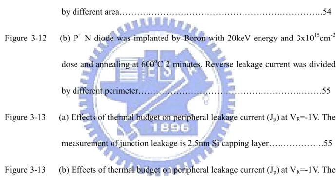
Figure 1.1 Measured and simulated IG-VG characteristics under inversion conditions of
SiO2 nMOSFETs [1]………6
Figure 1-2 The characteristics comparison with several depositing method………7
Chapter 2
Figure 2-1 MOSFET fabrication flow chart……….19 Figure 2-2 Effect of forming gas anneal (FGA) on 100 μm2 p+ n diodes with different
activations (a) 500℃ and (b) 550℃. The activations are done for 30s………20 Figure 2-3 Reverse current density at Vjunc= -1V with different FGA conditions………...21 Figure 2-4 Cross-sectional SEM images of Ni salmanide processes from IMEC. The SEM
image is published on 2008 Electrochem. Solid-State Lette……….21 Figure 2-5 The channel length dependent Id-Vg electrical characteristics of the 500℃ activated Ge PMOSFETs with different FGA temperatures. (a)w/o FGA, (b)w/300℃ FGA, (c) w/350℃ FGA, and (d)w/400℃ FGA………..22 Figure 2-6 The channel length dependent Id-Vd electrical characteristics of the 500℃
activated Ge PMOSFETs with different FGA temperatures. (a)w/o FGA, (b)w/300℃ FGA, (c) w/350℃ FGA, and (d)w/400℃ FGA………..23 Figure 2-7 Id-Vg characteristic of the Al2O3 PMOSFETs with 500℃ activation for three
different FGA temperatures……….24 Figure 2-8 Id-Vd characteristics of the Al2O3 PMOSFETs with 500℃ activation for three
different FGA temperatures……….24
Figure 2-9 (a) The effective mobility of the Ge PMOSFETs with different FGA temperatures.(b) References with HfO2/Ge (SP and SN) [12] and Ge/Si after PMA (H2) [13] are compared with our data………25
Figure 2-10 C-V characteristics of Ge PMOSFETs with different FGA at 500℃ act……...26 Figure 2-11 Id-Vg characteristics of the Al2O3 Ge PMOSFETs with 300℃ FGA for two
different activations………...27 Figure 2-12 Id-Vd characteristics of the Al2O3 Ge PMOSFETs with 300℃ FGA for two
different activations………...27 Figure 2-13 Vth characteristics of the Al2O3 Ge PMOSFETs with different FGA and
activation temperatures……….28 Figure 2-14 The Rm-Lg curves for extraction of RSD and ΔL. (a), (b), and (c) are different
activation………...29 Figure 2-15 The extraction of RSD and ΔL with different FGA conditions at 500 and
550℃……….30 Figure 2-16 (a) Dit calculated from the Conductance method. (b) Dit calculated from the
Charge pumping method………...31 Figure 2-17 Charge pumping current v.s Vg with different FGA temperatures was evaluated at f =1MHz………32 Figure 2-18 (a) The on/off ratio of Ge PMOSFETs with different FGA and activation
conditions. (b) Subthreshold swing of Ge PMOSFETs different FGA and activation conditions……….33 Figure 2-19 Dependence of (a) Id degradation and (b) Gm degradation on total stress time at
two kinds of inversion stress voltages for all Ge PMOSFETs………..34 Figure 2-20 Dependence of (a) threshold voltage shift and (b) SS on total stress time at two
kinds of inversion stress voltages for all Ge PMOSFETs……….35
Chapter 3
Figure 3-1 P+-N junc. fabrication flow chart………...44 Figure 3-2 TEM image of the capacitor cross section with SiH4 pretreatment. The bright
Figure 3-3 The leakage current equation and a simple diagram about the path of leakage current………..47 Figure 3-4 (a) This pn diode was implanted by Boron with 10keV energy and 1x1015cm-2 dose and annealing at 500oC 30s. Reverse leakage current was divided by different area………...47 Figure 3-4 (b) This pn diode was implanted by Boron with 10keV energy and 1x1015cm-2 dose and annealing at 500oC 30s. Reverse leakage current was divided by different perimeter………..48 Figure 3-5 (a) P+ N diode was implanted by Boron with 10keV energy and 1x1015cm-2
dose and annealing at 500oC 2 minutes. Reverse leakage current was divided by different area………...48 Figure 3-5 (b) P+ N diode was implanted by Boron with 10keV energy and 1x1015cm-2
dose and annealing at 500oC 2 minutes. Reverse leakage current was divided by different perimeter………..49 Figure 3-6 (a) P+ N diode was implanted by Boron with 10keV energy and 1x1015cm-2
dose and annealing at 600oC 30s. Reverse leakage current was divided by different area………49 Figure 3-6 (b) P+ N diode was implanted by Boron with 10keV energy and 1x1015cm-2
by different perimeter………..50 Figure 3-7 (a) P+ N diode was implanted by Boron with 10keV energy and 1x1015cm-2
dose and annealing at 700oC 30s. Reverse leakage current was divided by different area………..50 Figure 3-7 (b) P+ N diode was implanted by Boron with 10keV energy and
1x1015cm-2dose and annealing at 700oC 2 minutes. Reverse leakage current was divided by different perimeter………...51 Figure 3-8 Effects of thermal budget on peripheral leakage current (Jp) at VR=-1V. The
measurement of junction leakage is 2.5nm Si capping layer……….51 Figure 3-9 Effects of thermal budget on junction leakage current at VR=-1V. The
measurement of junction leakage is 2.5nm Si capping layer……….52 Figure 3-10 (a) P+ N diode was implanted by Boron with 20keV energy and 3x1015cm-2 dose and annealing at 500oC 5 minutes. Reverse leakage current was divided by different area……….52 Figure 3-10 (b) P+ N diode was implanted by Boron with 20keV energy and 3x1015cm-2
dose and annealing at 500oC 5 minutes. Reverse leakage current was divided by different perimeter………....53 Figure 3-11 (a) P+ N diode was implanted by Boron with 20keV energy and 3x1015cm-2
by different area……….53 Figure 3-11 (b) P+ N diode was implanted by Boron with 20keV energy and 3x1015cm-2
dose and annealing at 500oC 10 minutes. Reverse leakage current was divided by different perimeter……….54 Figure 3-12 (a) P+ N diode was implanted by Boron with 20keV energy and 3x1015cm-2
dose and annealing at 600oC 2 minutes. Reverse leakage current was divided by different area……….54 Figure 3-12 (b) P+ N diode was implanted by Boron with 20keV energy and 3x1015cm-2
dose and annealing at 600oC 2 minutes. Reverse leakage current was divided by different perimeter………55 Figure 3-13 (a) Effects of thermal budget on peripheral leakage current (Jp) at VR=-1V. The
measurement of junction leakage is 2.5nm Si capping layer……….55 Figure 3-13 (b) Effects of thermal budget on peripheral leakage current (Jp) at VR=-1V. The
Table Captions
Chapter 1
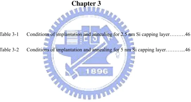
Table 1-1 Si, Ge, and GaAs properties at T=300 K [2]………..6
Chapter 3
Table 3-1 Conditions of implantation and annealing for 2.5 nm Si capping layer………46 Table 3-2 Conditions of implantation and annealing for 5 nm Si capping layer………...46
Chapter 1
Introduction
1-1 General Background
Over the last four decades, the dominate development of the semiconductor industry has been focused on silicon very-large-scale-integration (VLSI) technology. The sustained growth in VLSI technology is supported by the continued scaling of transistors to smaller dimensions. With the reduction in device dimensions of metal-oxide-semiconductor field effect transistors (MOSFETs), silicon dioxide (SiO2) films used as a gate dielectric have been scaled down to keep the same control over the channel. Devices with the thinner dielectric could improve the short channel effects. Therefore, the thickness of gate dielectric must continue to be scaled down for the gate length scaling. When the SiO2 thickness decreases to less than 20Å, the gate leakage current density becomes significantly high (>1A/cm2) because of the direct tunneling effect, as show in Fig 1.1, which shows measured and simulated IG-VG characteristics under inversion conditions of SiO2 nMOSFETs [1]. Hence it has become apparent that the continued scaling of Si CMOS devices would finally lead to a physical obstacle. Therefore, various approaches are being investigated to alleviate the tremendous pressure on continuously improving the performance of scaled device. One of the solutions is that we can use high
dielectric constant (high-k) materials to replace SiO2. Because high-k dielectrics can be several times thicker than SiO2, they reduce gate leakage by over 100 times. Another is using higher carrier mobility as channel materials such as Ge or Ш-V compounds. In the recent years, Ge attracts great attention because it offers higher electron (2.5x) and hole mobility (4x) than Si, as shown in Table 1.1. However, from the technology point of view, the developments of Ge MOSFETs have been blocked for decades due to the absence of a good thermally grown oxide on Ge. Recently, the successful development of high-k dielectrics on Si has facilitated the development of the Ge MOSFETs because it demonstrates that the gate dielectrics are no longer restricted to the thermal oxide. There have been many reports on Ge MOS structures using Al2O3 [3], HfO2 [4], Dy2O3 [5], HfON, and ZrO2 [6]. However, there is an intrinsic problem in the formation of the gate dielectric on Ge substrate. Germanium oxide is thermally unstable, and water soluble. Hence, minimizing the formation of GeOx at the interface between high-k dielectric and Ge substrate is a critical issue to form high quality stack on Ge. Surface treatments before high-k dielectrics deposition is one of the solution for the problem. Surface treatments include annealing Ge in an NH3 ambient and annealing in a SiH4 ambient. The second way removes the native germanium oxide and passivates the germanium surface by an ultra-thin Si cap. They were also reported to be essential to achieve better device performance. Furthermore, Ge had several intrinsic problems such as the band-gap in Ge is smaller than in Si and the intrinsic carrier concentration in Ge is three
orders higher than in Si. They would lead to the higher reverse leakage current. Another, the density of Ge is 3 times heavier than Si such that Ge bulk wafers were applied to Si process equipment is a big challenge.
1-2 Motivation
In order to continuously improve the performance of scaled device, Ge substrates have been used. However, Ge has several practical problems. First, unlike Si, Ge lacks a sufficiently stable thermally grown oxide. Ge oxides (e.g. GeOx and GeO2 ) are either water soluble or volatile, they are easily rinsed off or sublime during the fabrication process [7], [8]. Second, Ge/oxide interfaces are known to exhibit lower quality than Si/oxide interfaces and results in a difficulty to form a gate stack structure on Ge with good interface qualities. Third, Ge has a much smaller direct band gap compared to Si which may give rise to higher leakage.
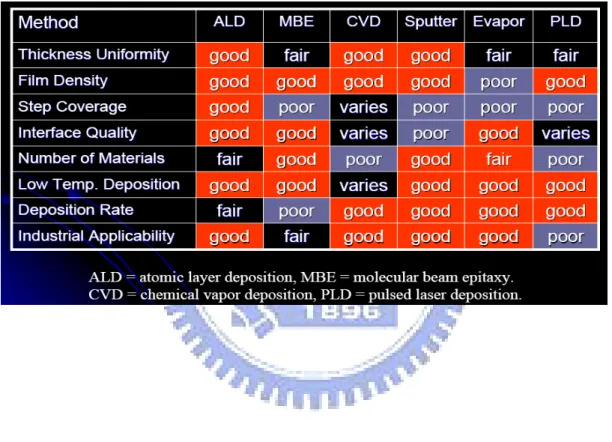
Recently, germanium MOS structures with high-k gate dielectrics have been reported. It demonstrates that the gate dielectrics are no longer restricted to the substrate’s thermally grown oxide. We adopt atomic layer deposition (ALD) system to grow Al2O3 as the gate dielectric. Atomic layer deposition (ALD) system has lots of excellent abilities, such as almost 100% step coverage, accurate thickness control, large area uniformity, excellent
process stability, and low processing temperatures. Atomic layer deposition (ALD) system just has only one problem is that the slower deposition rate. But we can use the multi-chamber to solve this problem. We chose the Al2O3 as the gate insulator due to the similarities of the band-gap, band alignment and thermal stability material characteristics to the SiO2. Also, Al2O3 has a higher dielectric constant value about 2.5 times than SiO2.
Hydrogenation can be used to significantly decrease the density of interface states, with most of the improvements resulting from passivating the Si dangling bonds (DB) through the formation of Si-H bonds [9]. A recent study reported that high temperature forming gas anneal (FGA) treated on Ge showed significant improvements in the carrier mobility, drive current, and subthreshold slopes of metal-oxide-semiconductor field-effect transistors with HfO2 gate stack [10]. These improvements can be attributed to the improvements of the interface quality by lowering both interface state density and interface charges.
In our thesis, we employed the low-temperature forming gas anneal to improve the interface between the Ge substrate and high-k gate dielectrics. It is found that the low-temperature (≦ 400℃) forming gas anneal can also improve the interface quality by slightly reducing the Dit. The reduction of Dit can improve the drive current, subthreshold slope, effective mobility (μeff) and transconductance (Gm). The improvements are represented in the chapter 2. Finally, we used the ultra-thin Si capping layer on the top of Ge channel to prevent Ge native oxides from forming (e.g. GeOx and GeO2). Furthermore, it can also decrease the number of the interface
state density and increase both the effective mobility (μeff) and drive current [11].
1-3 Organization of the thesis
In this thesis, it can be divided into two parts. First, we fabricated the pMOSFETs with the Ge bulk and ALD Al2O3 as the gate dielectric in different FGA temperatures ; then, we measure the essential electrical performances, constant voltage stress (CVS) , and charge pumping of Ge pMOSFETs which is the first part in Chapter 2. In the second part, using the strained-Ge on partially relaxed SiGe, we finish the fabrication of the pn junction formation with different dosages and energy of implantation as well as different annealing temperatures and times.
Figure 1.1 Measured and simulated IG-VG characteristics under inversion conditions of SiO2 nMOSFETs [1].
sub. material Ge Si GaAs
μp (cm2/ V- s) 1900 480 400
μn (cm2/ V- s) 3900 1350 8500
Eg (eV) 0.66 1.12 1.42
ni (cm-3) 2.4x10¹³ 1.5x10¹⁰ 1.8x10⁶
ε 16 11.7 13.1 native oxide GeOx SiO2 As2O3 ,Ga2O3
density (g/cm3) 5.33 2.33 5.32
Table 1-1 Si, Ge, and GaAs properties at T=300 K [2].
Chapter 2
Low temperature Forming Gas Anneal with Ge
p-MOSFETs
2-1 Introduction
In Chapter 2, we investigated the forming gas annealing (FGA) on the electrical characteristics of Ge PMOSFETs. First of all, we should understand the reason why we employed FGA technique. Owing to the interface quality between Ge substrate and high-k gate dielectric poor than Si, this degrading phenomenon led to reduce carrier mobility and accordingly lower the operating speed of devices. Then, we employed FGA technique to improve the problem of interface quality. It was reported that high-temperature (500~600°C) FGA successfully improved the interface quality between Si substrate and high-k gate dielectric [10]. From this report, we knew that high-temperature FGA had been found to be effective in improving the interface quality by lowering both interface state density (Dit) and interface charge. After FGA, the interface state density (Dit) was reduced 4 times. A few years later, high-temperature FGA on the GeOI substrates has been reported [12]. From this report, we knew that the devices after high-temperature FGA exhibited the better carrier mobility, with the interface trap density and the interface fixed charge as low as 1010q/cm2. However,
the previous reports are in reference to high-temperature (>400°C) for Ge devices. In this chapter, we used low-temperature (≦400°C) FGA on the Ge pMOSFETs. We found that the devices can be improved in many aspects such as sub-threshold slop, Dit, on-off ratio after low-temperature FGA. At the beginning, we showed the characteristics of pn junction after FGA (300, 350, 400 °C). We found that the better FGA temperature is 300 °C because of the lower junction leakage current. Then, we showed the electrical characteristics, such as Id-Vg, Id-Vd, and C-V, and discussed the parameters extracted from the essential electrical measurements, such as sub-threshold swing (S.S), threshold voltage (Vth), source drain series resistance (RSD), dopant in-diffusion length (△L), and effective mobility (μeff). We also utilized two methods- Conductance method, and Charge-Pumping to estimate the number of Dit exists near the substrate surface.
2-2 Experimental Procedures
The starting wafers for the experiments were Sb-doped (concentration~1.5x1014cm-3) with a resistivity of 8-13 Ohm cm. The native oxide (GeOx) was removed by dipping the samples in a diluted HF solution (HF:H2O=1:30) for 5 minutes, followed by rinsing in de-ionized water (D.I water) 10 minutes and N2 drying. After that, we used a plasma enhanced chemical vapor deposition (PECVD) system to deposit the field oxide SiO2 (thickness~4200 Å). Then, we defined the source drain(S/D) region by Mask 1 and etched SiO2 by Buffer Oxide Etching (BOE). To form a boron (B) doped P+-N junction region for restricting the flow of drain current just under the surface, the samples were implanted B+ with tilt: 7o and twist: 22o. The implant energy was 60 keV while the implant dose was 1x10¹⁵ atoms/cm2. Before removing the dummy gate by Mask 2, we activated the B-doped region. Annealing of the samples was performed in a N2 atmosphere in the JETFIRST RTP system at 500 °C or 550 °C annealing temperatures. As soon as the dummy gate was removed, we used an atomic-layer-deposition (ALD) system to grow the gate dielectric (Al2O3) at ~170 °C with 100 deposition cycles in Instrument Technology Research Center (ITRS). In this ALD system, tri-methyl-aluminum (TMA), Al(CH3)3, and H2O were chosen as the metal source and oxidant that were pulsed alternatively into the chamber for 1 sec; and per pulse separated by N2 purge of 10 sec to remove residual reactants during the process. During each cycle, the chamber was held at a
coated aluminum (Al) on the wafers with the help of thermal coater. After that coating was done, we used the Mask 4 to define the metal pads. For further improving the device characteristics, some Ge devices were treated in forming gas annealing (FGA) (N2/H2, 95:5 %) at 300, 350 and 400 °C for 30 minutes. The overall fabrication processes of the Ge p-MOSFETs were illustrated in Figure 2-1. After the fabrication of pMOSFETs, we measured the capacitance-voltage (C-V) and current-voltage (I-V) characteristics by Agilent 4284 LCR meter and Keithley 4200 semiconductor characterization, respectively. From the Id-Vg curves, the main parameters of devices, such as threshold voltage (Vt), On-Off ratio, and subthreshold swing (SS), were obtained. We also estimated the density of interface state (Dit) from G-V characteristic and charge pumping. In order to investigate the degradation of the device performances, they were undergone a constant gate voltage stressing (CVS) at -3V and -3.2V.
2-3 Results and Discussion
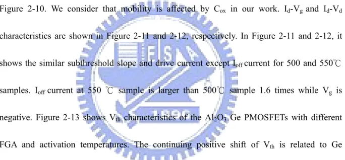
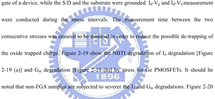
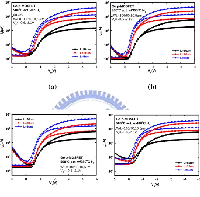
Figure 2-2 illustrates the effect of forming gas anneal (FGA) on 100 μm2 p+ n diodes with different activation conditions. (a) 500℃ and (b) 550℃. The activations were done for 30s. We find that the forward current density in our cases is lower than others had been reported [13]. We think the cause of lower forward current is the lower bulk doping level. The lower bulk doping level leads the higher series resistance and reduces the forward current. And the lower bulk doping level also brings out the higher reverse leakage current. Because the lower bulk doping level causes the huge bulk generation current such that the higher leakage current in our samples. From (a), we find that the reverse current of the p+ n diode after 300℃ FGA is smaller than non-FGA sample while forward current is almost equivalent to others. While the FGA temperature is larger than 300℃ (350 and 400℃), the reverse current is increased immediately.Specially, the reverse current of 400℃ FGA is one order than non- FGA sample at Vjunc.=-1V. We can see the analogous effect from Fig 2-2 (b). Figure 2-3 illustrates the reverse current density at Vjunc= -1V with different FGA conditions. As we have mentioned, the reverse current density are increased after higher FGA temperature (>300℃). The reverse current after 300℃ FGA is reduced because of the decrease of the defects. Forming gas annealing ambient is H2 and N2. Hydrogen (H2) is confirmed to passivate the defects such that
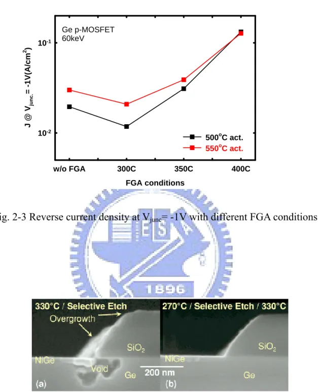
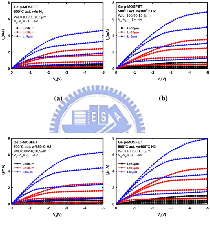
the reverse current reduced. The reason for the increasing reverse current after higher FGA temperature (>300℃) is that Ge out-diffusion and Al incorporation in Ge bulk introduce defects near the p+ n junction. Figure 2-4 is published on 2008 Electrochem. Solid-State Lette. from IMEC and ASM Belgium [14]. It shows that the temperature >300℃, large-scale Ge voiding and germanide overgrowth occur because of the out-diffusion of Ge. Figure 2-5 and 2-6 are the channel length dependent Id-Vg and Id-Vd electrical characteristics of the 500℃ activated Ge PMOSFETs with different FGA temperatures, respectively. Id-Vg characteristic of the Al2O3 PMOSFETs with 500℃ activation for three different FGA temperatures is shown in Figure 2-7. It shows some interesting events in Figure 2-7. First, Ioff current is decreased after 300℃ FGA compared to non- FGA sample. However, Ioff current is increased after higher FGA temperature (400℃) compared to non- FGA sample and 300℃ FGA sample. Second, the 300℃ FGA sample has the steeper slop when Vd is small. Finally, we can find that forming gas annealing shifts the curves of Id-Vg. We explain the results in order. The reduction of Ioff current after 300℃ FGA is attributed to H2 passivates the interface state density (Dit: 7.53x10¹¹ eV-1cm-2 after 300℃ FGA vs. 1.07x10¹² eV-1cm-2 before) and improve the p+ n junction. But the higher temperature (400℃) introduces Ge out-diffusion in p+ n junction such that Ioff current is increased. The steeper slope of Id-Vg curve after 300℃ FGA is attributed to the lower Dit. Finally, the shift of the Id-Vg curve is attributed to threshold voltage shift. Id-Vd characteristics of the Al2O3 PMOSFETs with 500℃ activation for three different
FGA temperatures are shown in Figure 2-8.
Based on the first order current-voltage approximation, the drive current ID for a MOSFET in the saturation region can be written as below
(1.1)
Where Cox is the gate oxide capacitance and mainly determined by the permittivity and the thickness of the gate insulator. μn is the mobility for the electrons or holes. W and L are the channel width and length, respectively. VGS is the applied gate-to-source voltage, and VT is the threshold voltage. From the above equation, the drain current Id is affected by Cox and μn. The higher drain current Id after FGA is illustrated in Figure 2-8. We mainly attribute the higher drain current Id to higher mobility and increasing Cox. However, the higher mobility is attributed to the lower Dit and the lower S/D series resistance. The effective mobility of the Ge PMOSFETs with different FGA temperatures are illustrated in Figure 2-9(a). References with HfO2/Ge (SP and SN) [15] and Ge/Si after PMA (H2) [16] are compared with our data are illustrated in Figure 2-9(b). The extracted effective hole mobility of the MOSFETs equation is mentioned as below:
Where Qn= Cox (VGS-VT) and the drain conductance gd is defined as
Cox is obtained by C-V measurement for Ge PMOSFET at f (frequency)=10 kHz and gd is obtained by Id-Vg at Vd=-50 mV. From Figure 2-9(a), we find that the mobility after FGA is larger than non-FGA. Specially, the mobility after 400℃ FGA is almost 2 times than non-FGA in all electric field. We can find that our device characteristics are not bad in comparison with others in Figure 2-9(b). However, the Cox is higher after FGA is showed in Figure 2-10. We consider that mobility is affected by Cox in our work. Id-Vg and Id-Vd characteristics are shown in Figure 2-11 and 2-12, respectively. In Figure 2-11 and 2-12, it shows the similar subthreshold slope and drive current except Ioff current for 500 and 550℃ samples. Ioff current at 550 ℃ sample is larger than 500℃ sample 1.6 times while Vg is negative. Figure 2-13 shows Vth characteristics of the Al2O3 Ge PMOSFETs with different FGA and activation temperatures. The continuing positive shift of Vth is related to Ge out-diffusion [17], [18], [19]. Two possible incorporation mechanism: (a) out-diffusion of gaseous GeO species from the substrate and downward into the high-k layer through airborne transportation and (b) GeO volatilization from the IL and top surface of the Ge substrate [19]. The incorporation mechanism possibly causes VFB shift by inducing negative fixed charges near the interface and into the dielectric.
(1.3)
Where Rch is channel resistance and RSD is source drain (S/D) series resistance. Figure 2-14 shows the Rm-Lg curves for extraction of RSD and ΔL. (a), (b), and (c) are different FGA temperatures at 500℃ activation. (d) is 300℃ FGA with 550℃ activation. We find that the S/D series resistance is reduced after FGA. The S/D series resistance of as-deposited sample is 194Ω and 400℃ is 123Ω. The decreasing S/D series resistance attributes to higher temperature improves the interface between the Ge substrate and metal pads by the formation of alloy. However, the reducing S/D series resistance improves the drive current (ID) and effective mobility (μeff) as mentioned previously. It is illustrated in Figure 2-15 that the extraction of RSD and ΔL with different FGA conditions at 500 and 550℃. Figure 2-16 (a),(b) show Dit calculated from the Conductance and Charge pumping method, respectively. We can find the similar trend from the two figures. After 300℃ FGA, Dit is reduced slightly and Dit is increased after higher FGA temperature. It means that 300℃ FGA indeed improve the interface between the substrate and the gate insulator by H2 and higher FGA temperature (≧400℃) degrade the interface. Figure 2-17 shows charge pumping current v.s Vg with different FGA temperatures was evaluated at f =1MHz. We also find that the Icp current is decreased after FGA treatment in comparison with as-deposited sample. Figure 2-18 (a) shows the on/off ratio of Ge PMOSFETs with different FGA and activation temperatures. Ion and Ioff are extracted at Vth+0.8V and Vth-4V, respectively. The 300℃ FGA sample have higher value at on/off ratio about 103. However, the 400℃ FGA samples have the higher drive
current than others. As a result of the junction leakage, it degrades the on/off ratio. From Figure 2-18 (b), the minimum of sub-threshold slope of Ge PMOSFET is 300℃ FGA sample because of the minimum of Dit.
BTI is an important reliability issue of high-k gate dielectrics on silicon. Consequently, it is necessary to evaluate the BTI property of the high-k gate dielectrics on germanium. It is measured in MOSFETs biased under inversion. A negative voltage (Vstress) was applied to the gate of a device, while the S/D and the substrate were grounded. Id-Vg and Id-Vd measurement were conducted during the stress intervals. The measurement time between the two consecutive stresses was ensured to be minimal in order to reduce the possible de-trapping of the oxide trapped charge. Figure 2-19 show the NBTI degradation of Id degradation [Figure 2-19 (a)] and Gm degradation [Figure 2-19 (b)] by stress for Ge PMOSFETs. It should be noted that non-FGA samples are subjected to severer the Id and Gm degradations. Figure 2-20 show the NBTI degradation of Vth shift [Figure 2-20 (a)] and SS degradation [Figure 2-20 (b)] by stress for Ge PMOSFETs. It also represents that non-FGA samples have a higher Vth shift and SS increase in comparison with FGA samples. It means that non-FGA samples are subjected to NBTI degradation involves interface-trap generation. By employing FGA, Ge PMOSFETs show almost no change in sub-threshold swing. It suggests that the immunity from interface-trap degradation of Ge PMOSFETs could be achieved.
2-4
Summary
We already demonstrated a Ge bulk PMOSFETs by the standard 4 mask process. Most important parameters such as Id-Vg, Id-Vd, effective mobility, Vth, sub-threshold swing and so on are showed in this chapter. To further ensure the FGA technique can improve the interface between the Ge substrate and gate dielectric, we employed NBTI. It showed that 300℃ FGA can improve slightly the interface between Ge bulk and Al2O3 gate dielectric by lowering Dit. After 300℃ FGA, the S/D series resistance also reduced from 194 Ω to 181 Ω. Since the improvements of the interface quality and S/D contact, the drive current the mobility increased. But the higher temperature FGA (>300℃) introduced the Ge out-diffusion such that the junction leakage current increased. Although the junction leakage current increased, the S/D series resistance decreased significantly and the interface state density (Dit) increased slightly. After 400℃ FGA, it showed the highest mobility in comparison with others in our work. Stressing at Vg=-3.2 or -3V, it showed that FGA samples had smaller Vth shift, Id and Gm degradation and change of sub-threshold swing compared with non-FGA samples.
Dilute HF(HF:H2O=1:30,5 mins) and D.I. water 10 mins PECVD deposit Field Oxide
(thickness~4200 A)
Define the S/D region(1stMask)
Implantation(B+,60KeV,1e15cm-2)
Dopant activation (550℃,550 ℃)
Active area opening (2nd Mask)
ALD Al2O3deposition (~170 ℃)
Contact hole opening (3rdMask)
Al metallization (thermal coater)
Define metal pads (4thMask)
Ge substrate FOX P-N junction Al2O3 film Al Al Al FOX FOX
Forming gas annealing (~5% H2,95% N2;30 mins)
Fig. 2-2 Effect of forming gas anneal (FGA) on 100 μm
2p
+n diodes with
different activations (a) 500℃ and (b) 550℃. The activations are done for 30s.
Ge p-MOSFET 500oC act. 60keV Vjunc.(V) -2 -1 0 1 2 J(A/cm 2 ) 10-4 10-3 10-2 10-1 100 101 102 w/o H2 w/300oCH 2 w/400oCH2 w/350oCH2 Ge p-MOSFET 550oC act. 60keV Vjunc.(V) -2 -1 0 1 2 J(A/cm 2 ) 10-4 10-3 10-2 10-1 100 101 102 w/o H2 w/300oCH2 w/400oCH2 w/350oCH 2
(a)
(b)
Fig. 2-3 Reverse current density at V
junc= -1V with different FGA conditions.
Fig. 2-4 Cross-sectional SEM images of Ni salmanide processes from IMEC.
The SEM image is published on 2008 Electrochem. Solid-State Lette.
Ge p-MOSFET 60keV FGA conditions w/o FGA 300C 350C 400C J @ V junc . = -1V(A/ cm 2 ) 10-2 10-1 500oC act. 550oC act.
(a) (b)
(c) (d)
Figure 2-5 The channel length dependent I
d-V
gelectrical characteristics of the
500℃ activated Ge PMOSFETs with different FGA temperatures. (a)w/o FGA,
(b)w/300℃ FGA, (c) w/350℃ FGA, and (d)w/400℃ FGA.
Ge p-MOSFET 500oC act. w/o H2 60 keV W/L=100/50,10,5 μm Vd= -0.6,-2.1V Vg(V) -5 -4 -3 -2 -1 0 1 Id (μ A) 100 101 102 103 104 L=50um L=10um L=5um Ge p-MOSFET 500oC act. w/300oC H2 W/L=100/50,10,5μm Vd= -0.6,-2.1V Vg(V) -5 -4 -3 -2 -1 0 1 Id (μ A) 100 101 102 103 104 L=50um L=10um L=5um Ge p-MOSFET 500oC act. w/350oC H2 W/L=100/50,10,5μm Vd= -0.6,-2.1V Vg(V) -5 -4 -3 -2 -1 0 1 Id (μ A) 100 101 102 103 104 L=50um L=10um L=5um Ge p-MOSFET 500oC act. w/400oC H2 W/L=100/50,10,5μm Vd= -0.6,-2.1V Vg(V) -5 -4 -3 -2 -1 0 1 Id (μ A) 100 101 102 103 104 L=50um L=10um L=5um
(a) (b)
(c) (d)
`
Figure 2-6 The channel length dependent I
d-V
delectrical characteristics of the
500℃ activated Ge PMOSFETs with different FGA temperatures. (a)w/o FGA,
(b)w/300℃ FGA, (c) w/350℃ FGA, and (d)w/400℃ FGA.
Ge p-MOSFET 500oC act. w/o H2 W/L=100/50,10,5μm Vg-Vth= -1~ -4V Vd(V) -5 -4 -3 -2 -1 0 Id (m A) 0 2 4 6 8 L=50μm L=10μm L=5μm Ge p-MOSFET 500oC act. w/300oC H2 W/L=100/50,10,5μm Vg-Vth= -1~ -4V Vd(V) -5 -4 -3 -2 -1 0 Id (m A) 0 2 4 6 8 L=50μm L=10μm L=5μm Ge p-MOSFET 500oC act. w/350oC H2 W/L=100/50,10,5μm Vg-Vth= -1~ -4V Vd(V) -5 -4 -3 -2 -1 0 Id (m A) 0 2 4 6 8 L=50μm L=10μm L=5μm Ge p-MOSFET 500oC act. w/400oC H2 W/L=100/50,10,5μm Vg-Vth= -1~ -4V Vd(V) -5 -4 -3 -2 -1 0 Id (m A) 0 2 4 6 8 L=50μm L=10μm L=5μm
Figure 2-7 I
d-V
gcharacteristic of the Al
2O
3PMOSFETs with 500℃ activation
for three different FGA temperatures.
Figure 2-8 I
d-V
dcharacteristics of the Al
2O
3PMOSFETs with 500℃ activation
for three different FGA temperatures.
Ge p-MOSFET 500oC act. 60keV W/L=100/5 μm Vd= -0.6,-2.1V Vg(V) -4 -3 -2 -1 0 1 Id (μ A) 100 101 102 103 104 w/o H2 w/300oC H2 w/400oC H2 Ge p-MOSFET 500oC act. 60keV W/L=100/5 μm Vg-Vth= -1~ -4V Vd (V) -5 -4 -3 -2 -1 0 Id (m A) 0 2 4 6 8 w/o FGA w/300oC FGA w/400oC FGA
Figure 2-9 (a) The effective mobility of the Ge PMOSFETs with different FGA
temperatures. (b) References with HfO
2/Ge (SP and SN) [12] and Ge/Si after
PMA (H
2) [13] are compared with our data.
Weff/Leff=100/4 μm Electric Field (MV/cm) 0.0 0.1 0.2 0.3 0.4 0.5 Mobility (cm 2 /V s ) 0 50 100 150 200 250 Silicon Universality Black-No FGA Red-300oC FGA Blue-400oC FGA solid-500oC act. open-550oC act. Electric Field (MV/cm) 0.0 0.2 0.4 0.6 Mobility (cm 2 /Vs) 0 100 200 300 400 Silicon Universality 2006 IEDM HfO 2/Ge(SN)-2007 TED
HfO2/Ge(SP)-2007 TED
Our work: 500oC act. 400FGA
(a)
Figure 2-10 C-V characteristics of Ge PMOSFETs with different FGA at 500℃
activation.
(a)
Al/Al2O3/n-Ge sub.
Vg(V) -3 -2 -1 0 1 2 3 Capacitan ce ( μF/ cm 2 ) 1e-1 2e-1 3e-1 4e-1 5e-1 6e-1 7e-1 w/o FGA w/300oC FGA w/400oC FGA
Figure 2-11 I
d-V
gcharacteristics of the Al
2O
3Ge PMOSFETs with 300℃ FGA
for two different activations.
Figure 2-12 I
d-V
dcharacteristics of the Al
2O
3Ge PMOSFETs with 300℃ FGA
for two different activations.
Ge p-MOSFET w/300oC FGA W/L=100/5 μm Vd= -0.6,-2.1V Vg (V) -5 -4 -3 -2 -1 0 1 Id (μ A) 100 101 102 103 104 500oC act. 550oC act. Ge p-MOSFET 60keV w/300oC FGA W/L=100/5 μm Vg-Vth= -1~ -4V Vd (V) -5 -4 -3 -2 -1 0 I d (mA) 0 2 4 6 8 500oC act. 550oC act.
Figure 2-13 V
thcharacteristics of the Al
2O
3Ge PMOSFETs with different FGA
and activation temperatures.
Ge p-MOSFET W/L=100/5μm w/o H2 w/300C H2 w/400C H V th (V ) -0.5 -0.4 -0.3 -0.2 500oC act. 550oC act.
(a) (b)
(c) (d)
Figure 2-14 The R
m-L
gcurves for extraction of R
SDand ΔL. (a), (b), and (c) are
different FGA temperatures at 500℃ activation. (d) is 300℃ FGA with 550℃
activation.
Ge p-MOSFET 60keV
500oC act. w/o FGA
Channel length on mask (μm)
0 10 20 30 40 50 Rm (k Ω ) 0 2 4 6 8 10 RSD~194 Ω ΔL~0.51μm Ge p-MOSFET 60keV 500oC act. w/300oC FGA
Channel length on mask (μm)
0 10 20 30 40 50 Rm (k Ω ) 0 1 2 3 4 5 6 RSD~181 Ω ΔL~0.11μm Ge p-MOSFET 60keV 500oC act. w/400oC FGA
Channel length on mask (μm)
0 10 20 30 40 50 Rm (k Ω ) 0 1 2 3 4 5 RSD~123Ω ΔL~0.17μm Ge p-MOSFET 60keV 550oC act. w/300oC FGA
Channel length on mask (μm)
0 10 20 30 40 50 Rm (k Ω ) 0 1 2 3 4 5 6 RSD~160Ω ΔL~0.54μm
Figure 2-15 The extraction of R
SDand ΔL with different FGA conditions at 500
and 550℃.
Ge p-MOSFET Area=10-4 cm2 solid---500oC act empty---550oC act.w/o FGA w/300C FGA w/400C FGA
S /D R esis tance( Ω ) 100 120 140 160 180 200 Δ L 0.1 0.2 0.3 0.4 0.5 0.6
Figure 2-16 (a) D
itcalculated from the Conductance method. (b) D
itcalculated
from the Charge pumping method.
Ge p-MOSFET 60 KeV
W/L=100/50μm freq.=1M Hz
w/o FGA w/300C FGA w/400C FGA
Dit (eV -1 cm -2 ) 1011 1012 1013 1011 1012 1013 500oC act. 550oC act. Ge p-MOSFET 60 KeV W/L=100/50μm freq.=1M Hz
w/o FGA w/300C FGA w/400C FGA
D it (e V -1 cm -2 ) 1011 1012 1013 1011 1012 1013 500oC act. 550oC act.
(a)
(b)
Figure 2-17 Charge pumping current v.s V
gwith different FGA temperatures
was evaluated at f =1MHz.
Ge p-MOSFET 60 KeV W/L=100/10μm freq.=1M Hz Vg(V) -2 -1 0 1 2 3 I cp (μ A) 0 2e-1 4e-1 6e-1 8e-1 1e+0 open: 550oC act.closed: 500oC act. w/o FGA
w/300oC FGA
Figure 2-18 (a) The on/off ratio of Ge PMOSFETs with different FGA and
activation conditions. (b) Subthreshold swing of Ge PMOSFETs different FGA
and activation conditions.
Ge p-MOSFET W/L=100/5μm w/o H2 w/300C H2 w/400C H ON /OFF r a ti o(I on /I of f ) 102 103 104 500oC act. 550oC act. Ge p-MOSFET W/L=100/5μm w/o H2 w/300C H2 w/400C H Su bt hr e s h o ld sw in g (m V /d e c a d e ) 100 200 300 400 500 600 700 500oC act. 550oC act.
(a)
(b)
Figure 2-19 Dependence of (a) I
ddegradation and (b) G
mdegradation on total
stress time at two kinds of inversion stress voltages for all Ge PMOSFETs.
Stress time(s) 100 101 102 103 I degradationd (Δ Id /Id x100% ) -40 -30 -20 -10 0 500oC,w/o FGA 500oC,w/300oC FGA 550oC,w/300oC FGA closed: Vstress=-3V open: Vstress=-3.2V Stress time(s) 100 101 102 103 Δ Gm /G m (% ) -14 -12 -10 -8 -6 -4 -2 0 500oC,w/o FGA 500oC,w/300oC FGA 550oC,w/300oC FGA closed: Vstress=-3V open: Vstress=-3.2V
(a)
(b)
Figure 2-20 Dependence of (a) threshold voltage shift and (b) SS on total stress
time at two kinds of inversion stress voltages for all Ge PMOSFETs.
Stress time(s) 100 101 102 103 Δ Vth (m V) -500 -400 -300 -200 -100 0 500oC,w/o FGA 500oC,w/300oC FGA 550oC,w/300oC FGA closed: Vstress=-3V open: Vstress=-3.2V Stress time(s) 100 101 102 103 S u bthres hold s w ing(mV /decade) 150 200 250 300 350 400 500oC,w/o FGA 500oC,w/300oC FGA 550oC,w/300oC FGA closed: Vstress=-3V open: Vstress=-3.2V
(a)
(b)
Chapter 3
Electric characteristics of p
+-n junction of Si
1-xGe
x/Ge/Si
3-1 Introduction
We employed forming gas annealing (FGA) technique to improve the interface quality between the Ge substrate and the high-k gate dielectric such that the interface state density (Dit) is reduced slightly in Chapter2. As a result of the surface of Ge substrate is Ge bonds, Ge out-diffusion or oxygen inter-diffusion would be able to occur to form the low-k and poor electrical quality GeOx. It is necessary to employ pretreatment prior the deposition of high-k dielectrics. NH3 surface treatment [3] has been applied on high-k/Ge system to improve the electrical characteristics by forming GeOxNy interfacial later, but nitrogen incorporation may not be sufficient to fully passivate the dangling bonds on Ge surface and prevent the oxidation of the underlayer. It also induced positive fixed charges and a pretty high interface state density (Dit) [3]. Hence, it is reported that Si interlayer passivation on Ge is employed [17]. It is reported that a Si interlayer between a germanium substrate and a high-k gate dielectric, deposited using SiH4 gas at 580℃, significantly improved the electrical properities of Ge devices in terms of low Dit , less C-V hysteresis and frequency dispersion. However, we also employed the same technique of SiH4 pretreatment prior the deposition of Al2O3 gate
dielectric to passivate the Ge surface. But the result of SiH4 pretreatment in our work is not predicted as we thought to form a thin Si interlayer. It is replaced a thin Si interlayer by a thick Si layer. Figure 3-2 shows the cross section of the capacitor by high-resolution transmission electron microscope (TEM). The Si interlayer was deposited by PECVD at 400℃.The duration of SiH4 pretreatment was 10s. From Figure 3-2, we found that the thickness of Si layer at least is more than 10 nm. And the quality of this Si layer is not good. Hence, we employed ultra high vacuum chemical vapor deposition (UHVCVD) to deposit the thin Ge and Si layers. In Chapter 3, we investigated the pn junction properties of Si/SiGe/Ge/Si systems. In our work, we employed two kinds of thickness of top Si layer. The thicknesses of Si layers are 2.5 or 5 nm. The range of dosage in our experiment is 1~3x1015 cm-2. And the annealing conditions are 500~700℃.
3-2 Experimental Procedures
The following substrate will be used in Chapter 3 which is different from the substrate we used in Chapter 2. At the beginning, we fabricate the pn junction to find out the better conditions of the dosages, implantation energy, annealing temperatures and annealing times. The starting wafers for the experiments are 5 inch Si (001) nominal n-type substrate with a resistivity of 2-6 Ohm cm. Above the nominal n-type substrate, 40 nm virtual SiGe substrate, 7 nm epitaxial Ge layer and 2.5 or 5 nm epitaxial Si layers are deposited by UHVCVD. First, the substrate is used with the 2.5 nm Si layer, we break it into fragments. After breaking the fresh wafer into fragments, the native oxide is removed by dipping the samples in a diluted HF solution (HF:H2O=1:100) for 90 seconds, followed by rinsing with de-ionized water (D.I water) 5 minutes and drying with N2. After that, we use a plasma enhanced chemical vapor deposition (PECVD) system to deposit the field oxide SiO2 (thickness~4200 Å). Then, we define the implant region by Mask 2 as mentioned in Chapter 2 and etch SiO2 by Buffer Oxide Etching (BOE). To form a P+-N junction with a boron doping in the P+ region by restricting the flow of drain current just under the surface, the samples are implanted by B+ with tilt: 7o and twist: 22o. The implant energy are10, 20, and 40 keV while the implant dose is 1x10¹⁵ atoms/cm2. Before activating the implant region, we deposit the thin oxide SiO2 by PECVD to prevent the dopant from losing. Annealing of the samples are performed in a N2
ambient in the JETFIRST RTP system at 500°C , 600°C and 700°C annealing temperatures. The annealing times are 30 and 120 seconds in 500°C , while it is 30 seconds in 600°C and 700°C. After annealing, we use the Mask 2 to etch the thin oxide SiO2 and define the metal pads. Subsequently, we coat aluminum (Al) on the backsides of these samples. Finally, all samples are treated in forming gas annealing (FGA) (N2/H2, 95:5 %) at 300 °C for 30 minutes. The overall fabrication processes of the epitaxial Ge p+- n junctions were illustrated in Figure 3-1. After the fabrication of pn junctions, we measure the current-voltage (I-V) characteristics by Keithley 4200 semiconductor characterization. In order to find out the effects in electrical characterization with different dosages and annealing times, we fabricate the pn junction again using the wafer with the 5 nm Si layer. After finishing the pn junction, we find out the better conditions of p+-n.
3-3 Results and Discussions
Table 2-1 shows the conditions of implantation and annealing for 2.5nm Si capping layer. Note that we didn’t have the device about 600oC 40keV. And Table 2-2 shows the conditions of implantation and annealing for 5 nm Si capping layer. Note that we used two different dosages in case of 5nm Si capping layer. Then, we show an equation [20] about the leakage current and a simple diagram about the path of the leakage current in Figure 3-3. We could divide the leakage current into two items. One is area leakage current, the other is perimeter leakage current. First, we discussed 2.5nm Si capping layer at different annealing conditions and we only chose 10keV to discuss. Figure 3-4(a) shows pn diode is implanted by Boron with 10keV energy and 1x1015cm-2 dose and annealing at 500oC 30s. Reverse leakage current is divided by different area. We find that the reverse leakage current at different area are not closed. Figure 3-4(b) shows the same conditions of annealing and implantation except the pn junction is divided by different perimeter. We find that the junction current is divided by different perimeter are closed in comparison with area. Consequently, we think the peripheral junction current dominates the junction leakage. Figure 3-5(a) shows p+ n diode was implanted by Boron with 10keV energy and 1x1015cm-2 dose and annealing at 500oC 2 minutes. Reverse leakage current was divided by different area. The result of junction leakage was like Figure 3-4(a). And Fig. 3-5(b) shows p+ n diode was implanted by Boron with 10keV
energy and 1x1015cm-2 dose and annealing at 500oC 2 minutes. Reverse leakage current was divided by different perimeter. We found that the junction current was divided by perimeter is closed compared with area. It meant that the junction leakage is dominated by peripheral leakage current. We also found the same result in Figure 3-6(a) and Figure 3-6(b). Finally, we showed the p+ n junction is annealing at 700oC activation in Figure 3-7(a) and (b). The result of junction leakage, which one is dominated, peripheral junction leakage dominated the junction leakage. Then, we took all conditions into comparison in Figure 3-8. We found some interesting things. First, the peripheral leakage wasn’t affect by implantation energy. Second, the peripheral leakage current was mainly affected by annealing temperature. The leakage current was reduced almost 10 times after 700oC annealing compared with 500oC activation. Hence, we though that the domination of peripheral leakage current is the defects. Because, 500oC~700oC annealing temperatures on Si couldn’t repair the defects by implantation. The main source of junction leakage came from these un-repair defects. Figure 3-9 shows the leakage current at different thermal budget. The main effect of leakage current is still annealing temperature. Then, we discussed the electrical properties of the p+ n diode with 5nm Si capping layer. Since, we had two different dosages 1x10¹⁵, 3x1015 cm-2. But, we found that the exhibit of 1x1015 cm-2 with 2.5nm Si capping layer is same as 5nm Si capping layer. Here, we only discussed the result of 3x1015 cm-2 with 5nm Si capping layer. Figures 3-10(a) and (b) show p+ n diode were implanted by Boron with 20keV energy and 3x1015cm-2
dose and annealing at 500oC 5 minutes. Reverse leakage current was divided by different area and perimeter, respectively. We found that the similar result with 5nm Si capping layer. The reverse leakage current was dominated by peripheral current. Because, the reverse leakage currents were divided by different perimeters, where are more closely than different areas. Figures 3-11(a) and (b) show p+ n diode were implanted by Boron with 20keV energy and 3x1015cm-2 dose and annealing at 500oC 10 minutes. Reverse leakage current was divided by different area and perimeter, respectively. We also found the same condition in comparison with 500oC 5 minutes case. Figures 3-12(a) and (b) show p+ n diode were implanted by Boron with 20keV energy and 3x1015cm-2 dose and annealing at 600oC 2 minutes. Reverse leakage current was divided by different area and perimeter, respectively. Again, we found the similar result at annealing 600oC 2 minutes. Consequently, we thought the defects from implantation would not be able to repair in continuous annealing led to high reverse leakage current. Figures 3-13(a), (b) show the effect of thermal budget on peripheral leakage current (Jp) at VR=-1V. The measurement of junction leakage is 2.5 and 5nm Si capping layer, respectively. We found that the peripheral leakage current was similar to each other in the range of 10-3~10-2 (A/cm). But, the time of annealing with 5nm Si capping layer is longer than 2.5nm Si capping layer. Hence, we thought the thinner Si capping layer is better for Si/Ge/Si1-xGex substrate material.
3-4 Summary
We had shown the electrical properties with different Si capping layer thickness and thermal budget. From the electrical analysis, we found that peripheral leakage current dominated the reverse leakage current with 2.5 and 5nm Si capping layers. And we thought the defects in Si capping layer attributed to peripheral current. Since, 500oC~700oC could not repair defects from implantation. However, higher annealing temperatures ware not good for Ge channel. Hence, we could deposit the thinner Si (<1 nm) capping layer top of Ge channel. Because, the thinner Si layer can be consume in continuous processes and Si capping layer can be the passivation layer to passivate Ge surface to gain the better interface quality.
Wafer cleaning (DHF)
PECVD Field Oxide (thickness~4200 A)
Define implant region (1stMask)
Implantation(B+,10~40KeV)
Activation (500℃,600,700 ℃)
Back contact (Al)
Forming gas annealing (~5% H2,95% N2;30 mins)
Metal pads (Al)
FOX Al Al Si substrate epi-SiGe: 40nm epi-Si: 2.5 or 5 nm epi-Ge: 7 nm
Fig. 3-2 TEM image of the capacitor cross section with SiH
4pretreatment. The
bright layer is Al
2O
3. And under the Al
2O
3is Si interlayer.
Al
2O
3Si interlayer
SiGe/Ge/Si(40/7/2.5)nm Dose:1E15 cm-2 600oC 30s 700oC 30s 10 keV G L 20 keV H J 40 keV 500oC 30s 120s C F K
Table 3-1 Conditions of implantation and annealing for 2.5 nm Si capping layer.
SiGe/Ge/Si(40/7/5)nm 500oC 5 mins 500oC 10 mins 600oC 2 mins 20keV 1E15cm-2 40keV A D B E C F 20keV 3E15cm-2 40keV G J H K I L
Table 3-2 Conditions of implantation and annealing for 5 nm Si capping layer.
B E A D
Fig. 3-3 The leakage current equation and a simple diagram about the path of
leakage current.
Fig. 3-4(a) This pn diode was implanted by Boron with 10keV energy and
1x10
15cm
-2dose and annealing at 500
oC 30s. Reverse leakage current was
divided by different area.
JA JP JP
a
a
2I
R= J
Ax Area + J
Px Perimeter
(
a
2) (
4a
)
a
Boron, 1E15cm-2, 10keV
500oC, 30s Area ratio= 1:1.24:6.04 Voltage (V) -2 -1 0 1 2 I (A/ c m 2 ) 10-3 10-2 10-1 100 101 102 103 A=2.02x10⁻⁴cm2 A=2.5x10⁻⁴cm2 A=1.22x10⁻³cm2
Fig. 3-4(b) This pn diode was implanted by Boron with 10keV energy and
1x10
15cm
-2dose and annealing at 500
oC 30s. Reverse leakage current was
divided by different perimeter.
Fig. 3-5(a) P
+N diode was implanted by Boron with 10keV energy and
1x10
15cm
-2dose and annealing at 500
oC 2 minutes. Reverse leakage current
was divided by different area.
Boron, 1E15cm-2, 10keV
500oC, 30s Perimeter ratio= 1:1.16:2.36 Voltage (V) -2 -1 0 1 2 I (A/cm) 10-5 10-4 10-3 10-2 10-1 100 Peri.=0.0604 cm Peri.=0.07 cm Peri.=0.1424 cm
Boron, 1E15cm-2, 10keV
500oC, 2mins Area ratio= 1:1.24:6.04 Voltage (V) -2 -1 0 1 2 I (A/cm 2 ) 10-3 10-2 10-1 100 101 102 103 small medium large
Fig. 3-5(b) P
+N diode was implanted by Boron with 10keV energy and
1x10
15cm
-2dose and annealing at 500
oC 2 minutes. Reverse leakage current was
divided by different perimeter.
Fig. 3-6(a) P
+N diode was implanted by Boron with 10keV energy and
1x10
15cm
-2dose and annealing at 600
oC 30s. Reverse leakage current was
divided by different area.
Boron, 1E15cm-2, 10keV
500oC, 2mins Perimeter ratio= 1:1.16:2.36 Voltage (V) -2 -1 0 1 2 I (A/cm) 10-5 10-4 10-3 10-2 10-1 100 small medium large
Boron, 1E15cm-2, 10keV
600oC, 30s Area ratio= 1:1.24:6.04 Voltage (V) -2 -1 0 1 2 I (A/cm 2 ) 10-3 10-2 10-1 100 101 102 103 small medium large