國
立
交
通
大
學
電機學院 電子與光電學程
碩
士
論
文
應用於極寬頻之射頻高功率放大器設計與實現
Design and Implementation of Extremely Broad Band
RF High Power Amplifier
研 究 生:賴珀質
指導教授:郭建男 教授
應用於極寬頻之射頻高功率放大器設計與實現
Design and Implementation of Extremely Broad Band
RF High Power Amplifier
研 究 生:賴珀質 Student:Po-Chih Lai
指導教授:郭建男 Advisor:Dr. Chien-Nan Kuo
國 立 交 通 大 學
電機學院 電子與光電學程
碩 士 論 文
A Thesis
Submitted to College of Electrical and Computer Engineering National Chiao Tung University
in partial Fulfillment of the Requirements for the Degree of
Master of Science in
Electronics and Electro-Optical Engineering July 2013
Hsinchu, Taiwan, Republic of China
應用於極寬頻之射頻高功率放大器設計與實現 學生:賴珀質 指導教授:郭建男 國 立 交 通 大 學 電 機 學 院 電 子 與 光 電 學 程 碩 士 班 摘 要 射頻功率放大器是通訊系統中的關鍵元件,而寬頻的射頻功率放 大器更有高於一般的設計難度,且通常為系統中最昂貴的硬體,除了 在通訊系統外,雷達與高階醫療儀器中亦常見寬頻的射頻功率放大器 的使用. 本論文揭櫫一種適用於 VHF 延伸至部份 L 波段的極寬頻射頻高功 率放大器設計方法,採用擁有高功率密度的氮化鎵電晶體作為功率元 件,利用非線性模型進行模擬設計,並用 FR4 電路板實現驗證與調測, 設計的挑戰在於需同時間兼顧頻寬與輸出功率,量測結果顯示頻寬可 由 150 MHz 延伸至 1200 MHz,飽和功率可達 5 瓦,效率超過 40%.
Design and Implementation of Extremely Broad Band RF High Power Amplifier
Student: Po-Chih Lai Advisors:Dr. Chien-Nan Kuo
Degree Program of Electrical and Computer Engineering
National Chiao Tung University
ABSTRACT
Many wireless communication transceivers, radars and medical instruments involve RF power amplifier. To design a narrow band RF power amplifier is difficult, but to design a broad band RF power amplifier is even more challenged. This thesis introduces a method to design an extremely broad band RF power amplifier frequency ranging from VHF through UHF to lower L band.
A GaN HEMT is used to construct this power amplifier because of the intrinsic broad band and high power characteristic. To achieve such low Q in the pass band, a low pass type Bridged-T input matching network is adopted. Resistive feedback between the gate and the drain is used to enhance the gain flatness. The output matching network is implemented with LC sections optimized for broad band performance. The measurement data shows bandwidth ranging from 150 MHz to 1200 MHz, 5 W saturation output power, and PAE over 40%.
致謝 能完成這篇論文首先要感謝的是指導教授郭建男博士,能包容我 以在職的身分,一路走走停停、步履闌珊地走到了今天,老師許多的觀 點和建議讓我在研究和工作的專業領域上都受益良多!感謝口試委員 溫瑰岸教授與施鴻源博士的諸多建議與指導!也感謝實驗室的夥伴們, 俊興、子超、勁夫、家愷、志維、偉智和奕豪在研究上的討論和協助!
Contents
Abstract (Chinese)……….…...…………...………..i Abstract (English)………...…….ii Acknowledgement………...iii Contents………...……iv List of Tables………..………....….vii List of Figures………...……….viii Chapter 1 Introduction………11.1 The application of broad band RF power amplifiers………..1
1.1.1 Software defined radio ………...…1
1.1.2 Radar application………...2
1.1.2.1 Pulse radar………2
1.1.2.2 UWB radar………...3
1.1.2.3 Ground penetrating radar………..4
1.1.3 NMR magnetic field probing……….………...….……….4
1.1.4 CATV application………6
1.1.5 North American broadcast television………...……….6
1.2 The device technology of RF power amplifiers……….7
1.2.1 GaAs amplifiers………...7
1.2.2 Silicon amplifiers………7
1.2.3 GaN Amplifiers………...8
1.2.4 Device Level Technology Comparison………...8
Chapter 2 RF Power Amplifier Miscellanea …………...………12
2.1 RF power amplifier operation modes………...12
2.1.1 Linear Amplifier………....13 2.1.1.1 Class A Mode……….14 2.1.1.2 Class B Mode……….16 2.1.1.3 Class AB Mode………..17 2.1.1.4 Class C Mode……….17 2.1.2 Switching amplifiers……….19 2.1.2.1 Class D………...19 2.1.2.2 Class E………19 2.1.2.3 Class F………20
2.2 RF power amplifier terminologies……….21
2.2.1 Transducer Power Gain………..……….21
2.2.2 Gain Flatness………..…….21
2.2.3 Linearity………..22
2.2.3.1 1-dB compression……….22
2.2.3.2 Third-order intercept point………...…23
2.2.4 Efficiency………25
2.2.5 Power control………..25
Chapter 3 Broad Band Design Techniques………..27
3.1 Previous work on broad band power amplifiers………...27
3.2 Compressing Trajectory Dispersion Method………29
3.3 Multiple-Q Method (Chebyshev broad-banding technique)………32
3.4 Dummy bias technique……….35
Chapter 4 Practical Broad Band PA Design………41
4.1 GaN HEMT large-signal modeling introduction………..41
4.2 Bridged-T broad band design with large-signal model………....42
4.2.1 Bias consideration……….43
4.2.2 PA architecture……….…..44
4.2.3 PCB layout………45
4.2.4 Non-linear simulation with large-signal model……….……46
4.3 Verification and measurement………..50
4.3.1 Bias measurement……….50
4.3.2 Small signal measurement……….50
4.3.3 Environment setup for large signal measurement……….51
4.3.4 Large signal measurement………….………52
4.4 Result analysis and discussion……….55
4.5 Comparison with prior works………...………57
Chapter 5 Result analysis and discussion……….58
List of Tables
Table 1.1 Si, GaAs, SiC, and GaN material properties comparison……..……….…9
Table 1.2 Comparison of power density for production released devices…………..9
Table 1.3 Specifications of this work………...…….11
Table 2.1 Summary of power amplifier classes……….………...20
Table 3.1 Q curves, 2-section network, per transformation ratio. The Q curves are numbered from the outer most Q1 towards the inner Q3……….………32
Table 3.2 Q curves, 3-section network, per resistive transformation ratio. The Q curves are numbered from the outer most Q1 towards the inner Q3…...33
Table 3.3 Comparison of Broad Band PA Design Method……….…..40
Table 4.1 ADS non-linear simulation data @ P3dB………...………...…...48
Table 4.2 Raw data of Figure 4.21………....……55
Table 4.3 Achieved performances of this work @ Pin 27dBm………56
List of Figures
Figure 1.1 The UWB radar transmits in a very wide spectrum with very low
power………...4
Figure 1.2 Description of NMR frequency detection and calculation………...5
Figure 2.1 A basic PA topology………...………...…13
Figure 2.2 The I/V curve showing the bias point and load line for a transiston…..13
Figure 2.3 Class-A operation………...………...…..14
Figure 2.4 Class-A amplifier waveforms………..………...…15
Figure 2.5 Class-A amplifier waveforms………..…...……16
Figure 2.6 Class-B operation………...……….17
Figure 2.7 Q-point of Class-A, AB, B and C type amplifiers………..18
Figure 2.8 Conduction angle relations for linear amplifiers……….18
Figure 2.9 Block diagram showing definition of transducer power gain….………21
Figure 2.10 1-dB Compression characteristics………...…22
Figure 2.11 Corruption of signal due to nearby interferers………..…23
Figure 2.12 Third-order Intercept calculation………..………24
Figure 3.1 A simplified diagram of the balanced amplifier………..27
Figure 3.2 A simplified diagram of the distributed amplifier………...…..28
Figure 3.3 A simplified diagram of the feedback amplifier……….28
Figure 3.4 Z0=25, Q=1.75; node1-node2 shunt C=6.1pF; node1-node2 series L=3.8nH; red line marks the trajectory dispersing ranging from 800MHz to 1000MHz…………...………...….29
Figure 3.5 Z0=25, Q=1.75; node1-node2 shunt L=5.1nH; node1-node2 series
to 1000MHz………..30
Figure 3.6 50 to 3-ohm transformation; Z0 = 12.5, Q = 1.75; node1-node2 Shunt C = 6.10pF; node2-node3 Series L = 3.85 nH; node3-node4 Shunt L = 1.32 nH; node4-node5 Series C = 32.3 pF……..………31
Figure 3.7 Z0 = 12.3, SWR = 1.12 @ ZS = 3; N1-2 Shunt C = 6.9 pF; N2-3 Series L = 4.4 nH; N3-4 Shunt C = 30.4 pF; N4-5 Series L = 0.99 nH…………...…………..……….33
Figure 3.8 Z0 = 12.2, SWR = 1.01 @ ZS = 3; N1-2 Shunt C = 4.30 pF, N2-3 Series L = 6.22 nH; N3-4 Shunt C = 16.57 pF, N4-5 Series L = 2.42 nH; N5-6 Shunt C = 42.05 pF, N6-7 Series L =0.63 nH………...….34
Figure 3.9 Circuit diagram of dummy bias………35
Figure 3.10 A simple L type LC low pass filter………...36
Figure 3.11 A T type LC low pass filter………...………36
Figure 3.12 A T type LC low pass filter added a bridged capacitor………37
Figure 3.13 The prototype of the bridged-T matching Networks………38
Figure 3.14 Simplified FET linear model……….39
Figure 3.15 Further simplified FET model with equivalent input capacitance……39
Figure 3.16 Bridged-T network with simplified FET model………....40
Figure 4.1 ADS Schematic of bias sweeping………..….43
Figure 4.2 Result of bias sweeping………...…43
Figure 4.3 Diagram of the Bridged-T network extremely broad band PA…….…..44
Figure 4.4 PCB layout of the Bridged-T network extremely broad band PA……...45
Figure 4.5 PCB assembly of the Bridged-T network extremely broad band PA…..45
Figure 4.6 ADS Schematic of the Bridged-T network extremely broad band PA...46
Figure 4.7 The detail of the Bridged-T network in the ADS Schematic…………..47
Figure 4.9 The detail of the output matching network in the ADS Schematic….…48
Figure 4.10 The transducer power gain @ P3dB………...…….…….…49
Figure 4.11 Fundamental output power, 2nd and 3rd harmonic vs. frequency @ P3dB………...……….…..49
Figure 4.12 The picture of NPTB00004 Bridged-T Network extremely broad band PA PCB………..………50
Figure 4.13 S-parameter simulation and measurement data comparison…….……51
Figure 4.14 Diagram of large signal measurement setup………...51
Figure 4.15 Picture of large signal measurement setup………....52
Figure 4.16 Large signal measurement data @ 150MHz………...……..53
Figure 4.17 Large signal measurement data @ 300MHz………...…..53
Figure 4.18 Large signal measurement data @ 600MHz……….54
Figure 4.19 Large signal measurement data @ 900MHz...54
Figure 4.20 Large signal measurement data @ 1200MHz………...54
Chapter 1
Introduction
1.1 The application of broad band power amplifiers
Apart from the narrow bandwidth wireless application, the technical requirements of broad band application are much more rigorous. Plenty of niche apparatuses which need broad band power amplifiers are described in the following.
1.1.1 Software defined radio [1]
The Software-Defined Radio (SDR) architecture has been in existence for some time. Practical implementation on a larger scale has been made possible only recently due to the vast improvements in digital signal processing ICs and RF front end components. The components are similar to ones used in radio transceivers including modulator demodulators, frequency convertors, low noise amplifiers, and power amplifiers. The difference is that operation frequency modulation formats and encoding are purely determined by software. This offers the system the flexibility to adapt to the communication environment by scanning for available spectrum through software and optimizing the modulation format or radio standards to minimize interference. Significant cost savings are expected from increased spectral efficiency and from the ability to adapt to future standards. The key enablers for SDR include broad band linear front end components such as the power amplifier (PA)
and low noise amplifier (LNA), ADC and DACs for RF-to-digital to- RF conversion, and a high speed DSP for dynamic signal processing. Broad band and linearity requirements are critical to the ability of the SDR to adapt to multiple bands, modulation formats, and radio standards. For systems like the JTRS (Joint Tactical Radio System) and PMR (Public Mobile Radios), power amplifiers need to operate over multi-decade bandwidth covering VHF, UHF, and L-bands, and need to be highly efficient and compact, especially when the amplifier is used in a handheld or mobile unit. By using a single broad band PA instead of individual narrowband amplifiers for each band, significant cost savings are obtained through reduced component count by eliminating multiple PAs and its supporting bias, matching, switch and filter circuitry, further saving board real estate and reducing overall size. The PA requirements for portable and mobile SDR platforms range in power from a few watts to hundreds of watts, covering multi-octave and even multi-decade bandwidth while maintaining high efficiency.
1.1.2 Radar application
Microwave radar transmitters require PA which can magnify RF output power. Following items are the radars that require broad band PA.
1.1.2.1 Pulse radar
A pulse radar transmits a sequence of short pulses of RF energy. By measuring the time for echoes of these pulses scattered off a target to return to the radar, the range to the target can be estimated by the pulse radar. The major components of a pulse radar are the transmitter,
consisting of an oscillator and a pulse modulator, of course, a broad band PA also included; the antenna system, which passes electromagnetic energy from the transmitter to the transmission medium, and receives reflections from the target; the receiver, which amplifies the signal received by the pulse radar and detects returns from targets; and interfaces, including displays and interfaces to other electronic systems.
1.1.2.2 UWB radar
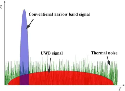
Ultra Wideband (UWB) radar systems transmit signals across a much wider frequency than conventional radar systems and are usually very difficult to detect. The transmitted signal is significant for its very light power spectrum, which is lower than the allowed unintentional radiated emissions for electronics. The most common technique for generating a UWB signal is to transmit pulses with very short durations (less than 1 nanosecond). The spectrum of a very narrow-width pulse has a very large frequency spectrum approaching that of white noise as the pulse becomes narrower and narrower. These very short pulses need a wider receiver bandwidth as conventional radar systems.
The amount of spectrum occupied by a signal transmitted by an UWB radar (i.e. the bandwidth of the UWB signal) is at least 25% of the center frequency. Thus, a UWB signal centered at 2 GHz would have a minimum bandwidth of 500 MHz and the minimum bandwidth of a UWB signal centered at 4 GHz would be 1 GHz. Often the absolute bandwidth is bigger than 1 GHz.
Figure 1.1 The UWB radar transmits in a very wide spectrum with very low power
1.1.2.3 Ground penetrating radar
Ground penetrating radar (commonly called GPR) is a geophysical method that has been developed over the past thirty five years for shallow, high-resolution, subsurface investigations of the earth. GPR uses high frequency pulsed electromagnetic waves (generally 10 MHz to 1,000 MHz) to acquire subsurface information. Energy is propagated downward into the ground and is reflected back to the surface from boundaries at which there are electrical property contrasts. GPR is a method that is commonly used for environmental, engineering, archeological, and other shallow investigations.
1.1.3 NMR magnetic field probing [2]
One of the primary requirements for effective Magnetic Resonance Imaging (MRI) is sufficient uniformity of the main magnetic field. Spatial homogeneity within a few ppm is never obtained without sophisticated correction systems ("shims"). The shimming process
requires a precise measurement and analysis of the magnetic field, which can be highly time consuming. One quick and easy way to measure the magnetic field is based on NMR probes with sweeping of the radio frequency. To measure the magnetic field from 0.08 Tesla to 7 Tesla, the radio frequency must be swept from 3.4MHz to 300MHz according toγ factor, 42.576255 MHz/T. The field is measured with a relative precision better than 0.1 ppm.
Normally, for each frequency sweep, resonance is detected twice, once on increasing, once on decreasing frequency. Then the mean value of these 2 counts is used to calculate the real NMR frequency.
Figure 1.2 Description of NMR frequency detection and calculation
1.14 CATV application
In North American cable TV networks, the radio frequencies used to carry signals to the customer are allocated from several tens MHz to around 1GHz. Since the cable network is a closed system, frequencies used for over-the-air services such as mobile radio, cellular telephone, or aircraft communications can be assigned to carry television programming. Slight frequency offsets are applied in some systems so that any signal leakage out of the cable distribution plant is less likely to cause objectionable interference to over-the-air users of the same frequencies. The main modulation scheme of CATV is QAM, implying good linearity required.
1.15 North American broadcast television
The North American broadcast television frequencies are on designated television channels numbered 2 through 69, approximately between 54 and 806 MHz. Traditionally, the frequencies are divided into two sections, the very high frequency (VHF) band and the ultra high frequency (UHF) band. The VHF band is further subdivided into two more sections, VHF-Lo (band I) and VHF-Hi (band III). In between lie allocations for other services including the FM broadcast band (band II), bands used for land mobile radio, radio remote control, civil service agencies, amateur radio, and aircraft navigation aids and voice ,communication (airband). All analog television systems use vestigial sideband modulation, a form of amplitude modulation in which one sideband is partially removed. In digital television systems, the modulation scheme is QAM and COFDM.
1.2 The device technology of power amplifiers [3]
This section introduces the devices such like GaAs, LDMOS and GaN. Each of the devices mentioned here surpass the others in its specialty domain. Finally, a comparison between GaAs, Si LDMOS and GaN technologies will show the advantages of each in broad band applications.
1.2.1 GaAs amplifiers
The GaAs devices include GaAs mesfet, GaAs pHEMT, GaAs HEMT and GaAs HBT. GaAs amplifiers are used as pre-drivers, drivers, and final stage amplifiers operating in microwave and millimeter frequencies. GaAs amplifiers operate in the 5V to 28V range. Power density limitations require either combining these devices, or excluding them from use in higher power applications where space limitations prohibit power combining.
1.2.2 Silicon amplifiers
Silicon amplifiers typically consist of silicon bipolar and Laterally Diffused Metal Oxide Semiconductor (LDMOS) technologies. These technologies are best known to operate at 28V, with new improvements up to 50V. This technology works well in VHF and UHF frequency ranges, but can also work up to 3.5GHz. Packaged modules using multiple die can offer power levels up to 1000W at 1GHz, but typical power levels are less than 200W. The intrinsic parasitic capacitance characteristics in this technology limit the bandwidth performance and power capabilities.
1.2.3 GaN Amplifiers
Gallium Nitride (GaN) amplifiers are deployed in high power wireless systems where design, manufacture, and adoption rates are increasing each year. For applications operating in frequency bands less than 6GHz, the manufacturers recognize that this wide-band gap technology offers significant advantages over existing Si and GaAs amplifiers. Advantages include higher voltage and broadband performance with high drain efficiency. There is increased GaN manufacturing activity in the U.S. and Japan toward higher frequency applications, (those greater than 10GHz), with emphasis on improvements in bandwidth, power output, and efficiency.
1.2.4 Device Level Technology Comparison
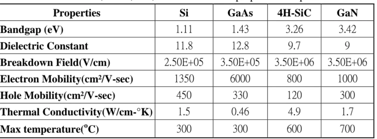
The data in Table 1.1 [4] allows a comparison of the most important performance metrics of silicon (Si), gallium arsenide (GaAs), silicon carbide (SiC), and gallium nitride (GaN). The larger thermal conductivity of SiC and GaN enables lower temperature rise due to self heating. The five to six times’ higher breakdown field of SiC and GaN is what gives those materials the advantage over Si and GaAs for RF power devices. Both GaN and SiC are wide bandgap materials, but only SiC suffers from poor electron transport properties, which hinders its use in very high frequency amplifiers. In addition, the wide bandgap gives devices the ability to operate at higher temperatures, and for some applications, allows devices to switch larger voltages.
Table 1.1 Si, GaAs, SiC, and GaN material properties comparison
Properties Si GaAs 4H-SiC GaN
Bandgap (eV) 1.11 1.43 3.26 3.42
Dielectric Constant 11.8 12.8 9.7 9
Breakdown Field(V/cm) 2.50E+05 3.50E+05 3.50E+06 3.50E+06
Electron Mobility(cm²/V-sec) 1350 6000 800 1000
Hole Mobility(cm²/V-sec) 450 330 120 300
Thermal Conductivity(W/cm-°K) 1.5 0.46 4.9 1.7
Max temperature(oC) 300 300 600 700
GaN HEMTs, GaAs pHEMTs, and Si LDMOS all have established positions in the broadband power amplifier application space. With any of these technologies the device manufacturer has many design variables that can affect performance dramatically. Among these are FET finger sizing and placement, epitaxial stack design, multi-die combining techniques, and packaging. Key performance properties of the three major RF power transistor technologies derived from production ready products are shown in Table 1.2 [5], [6].
Table 1.2 Comparison of power density for production released devices Item \ Device Nitronex 5W GaN 5W GaAs MESFET Nitronex 90W GaN 125W Si LDMOS CREE 6W GaN VDD 28V 28V 28V 28V 28V FET Periphery 2mm 4mm 36mm 180mm 1.2mm Power Density 2.5 W/mm 1.25W/mm 2.5 W/mm 0.7 W/mm 5W/mm
Comparing GaN to GaAs in the 5W power level shows that both technologies have sufficiently low load impedance Q and similar impedance transformation ratios. Both technologies are using the same drain voltage and both have minimal contribution of parasitics to the load
impedance. GaAs tends to have an advantage at higher frequencies as there are mature short gate length process nodes available. GaN has the advantages of improved thermal resistance and far higher output power capability.
Comparing GaN to Si LDMOS is more difficult. GaN has far higher power density which allows higher power levels to be put in a single packaged device. This reduces die-level parasitics and can allow for less complicated internal designs (smaller FET sizes) and therefore improved package parasitics and broader bandwidths. This results in a significant improvement in impedance transformation ratio. GaN is also a better high frequency technology and allows for higher frequency broad band designs to be realized. The lower power density of LDMOS has the advantage of inherently better thermal resistance. In some applications the power level achievable using GaN is limited by worst case junction temperature, therefore marginalizing the power density benefit.
GaN has a unique combination of high operating voltage and high power density, allowing broadband band high power designs than either GaAs FETs or Si LDMOS FETs. This is particularly interesting since current GaN HEMTs are first generation devices while both GaAs and Si are relatively mature technologies. The ability to develop higher power wideband designs with improved inherent robustness will continue to push GaN into an increasing number of applications. Future device generations will continue to widen this gap, making GaN an excellent fit for today’s broad band designs.
1.3 Design target
A broad band (from VHF to lower L band) and high power (>2 W) design is required, but deficient in the industry. The major goal of this thesis is to prove that such low Q (~0.6), broad band and high power board level RF power amplifier is available by using an unmatched GaN HEMT. Such PA can be used in the military FHSS SDR.
Table 1.3 Specifications of this work
Categories Specifications
Frequency range (MHz) 200 ~ 1200
Gain (dB) >10
Output power (dBm) >36
Chapter 2
RF Power Amplifier Miscellanea
No doubt the most expensive hardware component in a wireless communication system is the RF power amplifier. Though the RF power amplifiers had developed for a very long time and some of them were quite matured, many new architectures and devices still bloom and thrive because of new wireless communication technology launch. No matter how the new technology and devices are evolving, some fundamental categories and terminologies yet remain firm and erect.
2.1 RF power amplifier operation modes
In spite of there are different classifications for PAs, the most widely used is the distinction between linear and switching amplifiers. In linear amplifiers, the output amplitude of the signal is a linear function of the input amplitude. Class A, B, and AB amplifiers come under this type where the output transistor acts as a current source and the average output impedance during the operation is relatively high. The current and voltage waveforms through and across the output device are often full, or partial sinusoids. In switching amplifiers like Class-D, E and F, the power amplifier is driven with a large amplitude signal, turning the device ON or OFF as a switch. These amplifiers can achieve a very high efficiency at the expense of linearity.
OMN IMN VDD RFC D G S
Figure 2.1 A basic PA topology
2.1.1 Linear Mode Amplifier
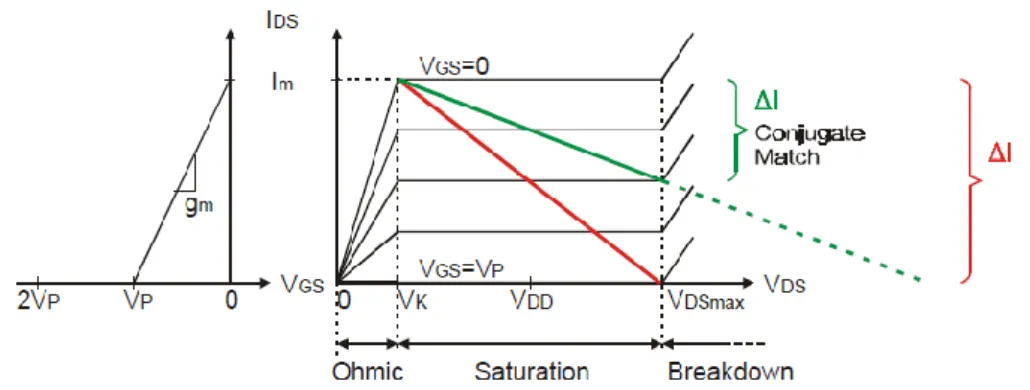
Linear amplifiers operate at constant gain and are based on the load-line theory [7], which states that the maximum power a transistor can deliver to a load is determined by the supply voltage and the maximum current of the transistor. When the transistor load is a large inductor/RF choke, the maximum voltage swing possible at the drain of this transistor is 2*supply voltage. The load line (of the optimum load resistance) for maximum output power is plotted from Ropt = VDSmax -
Vk / Im.
In other words, PAs can deliver maximum power to a load given by RLoad,opt. This resistance is then transformed to 50 Ω using an
impedance transformation network.
2.1.1.1 Class A
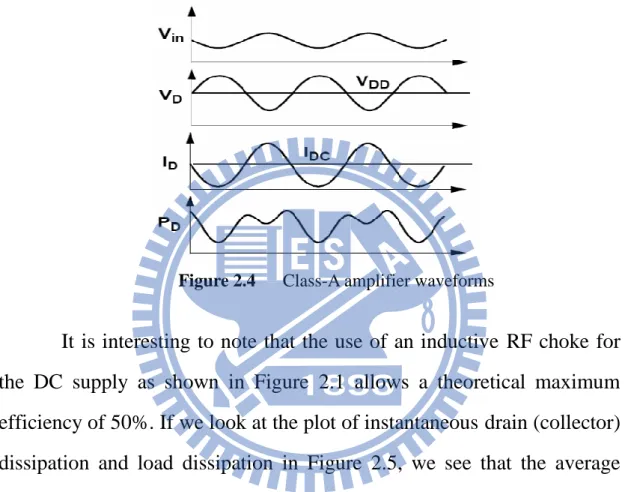
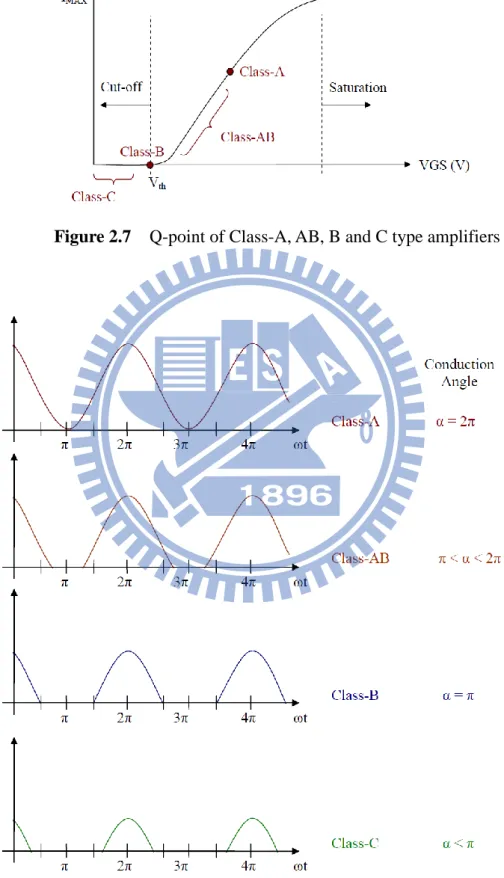
In class A, the quiescent current is large enough that the transistor remains at all times in the saturation (active) region and acts as a current source, controlled by the drive. Consequently, the drain voltage and current waveforms are (ideally) both sinusoidal. The Class-A amplifier is defined by a transistor that conducts current over the full 360 degrees of a cycle, 100% of the input signal is used. Class-A amplifiers are typically more linear and less complex than other types. The class of operation is determined by the operating point on the load-line i.e., from the I/V characteristics of the transistor. Figure 2.3 shows the bias point for a transistor in Class-A operation. Here the transistor is biased at the center of the load line i.e., the transistor is in the saturation (active) region at all times and the output voltage/current swings are maximum. The conduction angle α, which is the time for which the device is conducting, is equal to 2π in class-A amplifiers, as shown in Figure 2.8.
The voltage, current and power waveforms of a class-A amplifier are shown in Figure 2.4. As can be seen from the plots, the amplifier is always conducting, which results in a maximum efficiency of only 50%. However, the linearity is excellent as it preserves the input and output waveforms without any distortion.
Figure 2.4 Class-A amplifier waveforms
It is interesting to note that the use of an inductive RF choke for the DC supply as shown in Figure 2.1 allows a theoretical maximum efficiency of 50%. If we look at the plot of instantaneous drain (collector) dissipation and load dissipation in Figure 2.5, we see that the average power dissipated in the load and in the transistor drain (collector) are equal, hence the figure of 50%. As the transistor drain (collector) current decreases on the falling side of the wave, the DC source “pumps” power into the load circuit. As the transistor drain (collector) current increases, dissipation increases in the transistor and instantaneous power into the load decreases. The DC current from the supply remains practically constant. This is because the RFC inductor acts to smooth the current waveform.
Figure 2.5 Class-A amplifier waveforms
2.1.1.2 Class B
Class-B amplifiers are biased at the threshold voltage of the transistor such that the conduction angle is now π, as shown in Figure 2.8. The current waveform is positive only for one cycle of the input voltage. Hence the power consumption will be lower than class-A type. The optimal load resistance is now R
Load,opt = Vmax/(Imax), which is the same as
with Class-A type amplifiers. Theoretical efficiency is around 78%, but the linearity is worsened in these types of amplifiers. However, Class-B amplifiers also suffer from cross-over distortions at the switching points.
The gate bias in a class-B PA is set at the threshold of conduction so that (ideally) the quiescent drain current is zero. As a result, the transistor is active half of the time and thedrain current is a half sinusoid. Since the amplitude of the drain current is proportional to drive amplitude and the shape of the drain-current waveform is fixed, class-B provides linear amplification.
Figure 2.6 Class-B operation
2.1.1.3 Class AB
Class-A and B are two extremities of PA topologies in terms of efficiency and linearity. However, PA’s operating in the region between these two operating points is widely used and they are aptly known as class-AB amplifiers. Good linearity and efficiency can be achieved with devices in this regime. The conduction angle now is π <α<2 π.
2.1.1.4 Class C
Class-C amplifiers, which are non-linear, are biased below the cut-off region and their conduction angle is < π, as shown in Figure 2.8. With very low power consumption, the efficiency can reach up to 100%. However, the output power levels will also be quite low and unsuitable for most of the applications.
Figure 2.7 Q-point of Class-A, AB, B and C type amplifiers
2.1.2 Switch mode amplifiers
In switching amplifiers, the power amplifier is driven with a large amplitude signal, turning the device ON or OFF as a switch. They operate at constant input power (in saturated mode) and power control is obtained by varying the gain of the amplifier. Note that switching amplifiers are by definition non-linear with respect to the input signal; that is, amplitude information is not preserved.
2.1.2.1 Class D
Class-D PAs use two or more transistors as switches to generate a square drain-voltage waveform. A series-tuned output filter passes only the fundamental-frequency component to the load, resulting in power outputs of (8/π2
)VDD2/R and (2/π2)VDD2/R for the transformer-coupled and complementary configurations, respectively. Current is drawn only through the transistor that is on, resulting in 100 % efficiency for an ideal PA. A unique aspect of class D (with infinitely fast switching) is that efficiency is not degraded by the presence of reactance in the load. Practical class-D PAs suffer from losses due to saturation, switching speed, and drain capacitance. Finite switching speed causes the transistors to be in their active regions while conducting current. Drain capacitances must be charged and discharged once per RF cycle.
2.1.2.2 Class E
Class-E amplifiers are a relatively novel type of switching amplifier wherein the voltage and current waveforms are shaped using L’s
and C’s in such a way to achieve an efficiency of 100%. Under ideal condition, the voltage of the switch transistor drops to zero and has zero slope just as the transistor turns on and conducts current. This ensures that neither voltage nor current exists simultaneously in the circuit, thus achieving 100% efficiency. Class-E amplifiers require only a single transistor and can operate at frequencies as high as tens of GHz.
2.1.2.3 Class F
Class-F amplifiers employ harmonic resonators at the output to shape the drain waveforms. The harmonic traps are designed in such a way that the voltage waveform resembles a square wave (with the introduction of some harmonic components in the waveform) and the current wave resembles a half sine wave. Conversely, “inverse class-F” can also be designed. Again, both the voltage and current waveforms do not exist simultaneously, thus achieving good efficiency. With higher harmonics, the efficiency can be improved up to 100%, but linearity is severely worsened.
2.2 RF power amplifier terminologies
In this section, some of the important terms and specifications related to a PA are discussed.
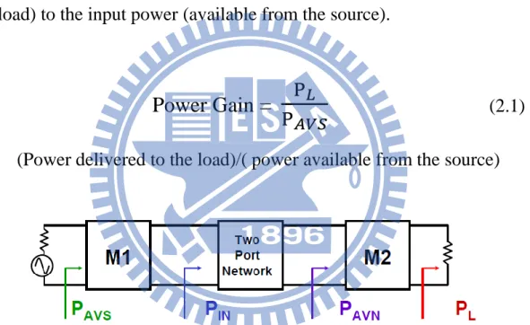
2.2.1 Transducer Power Gain
PA’s are required to boost the transmitted signal by providing a signal gain to the output of the preceding stage, usually a PA driver or a mixer. Transducer power gain is the ratio of output power (delivered to the load) to the input power (available from the source).
Power Gain =
(2.1)
(Power delivered to the load)/(power available from the source)
Figure 2.9 Block diagram showing definition of transducer power gain
2.2.2 Gain Flatness
This is the measure of uniformity of the gain across the wide frequency range of interest. This parameter commonly used for wide band systems. It is desired that the gain be flat over the frequency band.
2.2.3 Linearity
Linearity is an important metric of any amplifier. It is desired that the amplifier operate with high linearity i.e., the output power be linear with input power. However, a device eventually saturates after a certain input power, and this introduces harmonics in the output power spectrum. Linearity in power amplifiers is of serious concern because they can be often made to operate in the non-linear region to deliver a large output power. 1-dB compression and third order intercept points are typically used to measure linearity.
2.2.3.1 1-dB compression
As the name suggests, this is the input power at which the linear gain of the amplifier has compressed by 1 dB. The output referred 1-dB compression point (in dB) would then be given by the sum of the input referred 1-dB point (in dB) and the gain of the amplifier (in dB). This metric is a often used measure of the linear power handling capability of the PA.
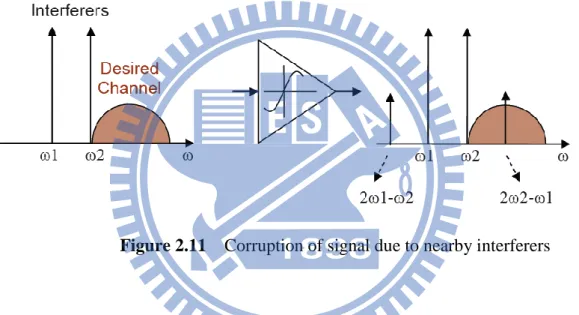
2.2.3.2 Third-order intercept point
This is a useful metric when comparing RF blocks with different specifications as it is independent of the input power levels. Assuming two interferers very close to the desired frequency, a non-linear output from the amplifier will generate inter-modulation products. The most important of the products is the third order product since it falls directly in the frequency band of interest. This situation is shown in Figure 2.11.
Figure 2.11 Corruption of signal due to nearby interferers
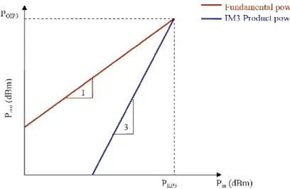
The amplitude of this IM3 product term increases in the order of cube of the fundamental amplitude and can be as significant as the fundamental tone after a certain input power. Figure 2.12 shows a plot of the IM3 product as a function of the input RF level. The third-order intercept point is the extrapolated intersection of this curve and the fundamental power. The input/output referred IP3 can be estimated from this plot.
Figure 2.12 Third-order Intercept calculation
Linearity can often be traded-off with efficiency depending on the class of operation. The choice of high linearity versus efficiency is based on the type of modulation used for transmission. For constant envelope modulation schemes like GMSK, FSK, the amplitude remains constant and the data is modulated using the phase of the carrier signal. Whereas in non-constant envelope modulation schemes like CDMA, the amplitude of the signal also carries some data information and hence it is important to maintain the exact shape of the signal without introducing any distortion through the power amplifier. Extremely linear power amplifiers are required for non-constant envelope modulation techniques, while the linearity can be traded-off for better efficiency in constant envelope modulation schemes.
Alternatively, techniques exist to improve the linearity while maintaining a good efficiency. Examples of such techniques are Doherty Amplifiers, Envelope elimination and restoration, Feed-forward technique, etc.
2.2.4 Efficiency
A measure of how efficiently the supply power is translated to output power is given by the efficiency.
(2.2)
A 100% η implies that the entire supply power is delivered to the load. However, this is practically impossible to achieve. The best way to improve the efficiency is the use of circuit techniques such that both voltage and current waveforms do not exist simultaneously. Switching amplifiers use this approach to achieve efficiencies up to 80%. However, as a trade-off, linearity needs to be compromised for better efficiency.
When comparing PAs with different input power levels, PAE (Power Added Efficiency) is a commonly used metric.
(2.3)
2.2.5 Power control
One of the many power saving schemes, especially in cellular systems, is the use of power control circuitry. When the mobile system is near a base-station, a decision logic at the output of the PA senses that high output power levels are not required and the control circuitry controls the amount of bias/supply to reduce the power levels. The reverse operation is performed when the base-station is at a distance away
η 𝑜𝑤𝑒𝑟 𝑑𝑒𝑙𝑖𝑣𝑒𝑟𝑒𝑑 𝑡𝑜 𝑡ℎ𝑒 𝑙𝑜𝑎𝑑 𝑜𝑤𝑒𝑟 𝑑𝑟𝑎𝑤𝑛 𝑓𝑟𝑜𝑚 𝑡ℎ𝑒 𝑠𝑜𝑢𝑟𝑐𝑒
from the mobile system. The battery life is thus improved, but at the expense of extra circuitry.
Chapter 3
Broad Band Design Techniques
To design a broad band amplifier, many specs other than bandwidth, such like output power, linearity, efficiency, etc., will be compromised in order to expand the operation bandwidth. In this chapter, several broad band design techniques are presented. Each of them has their unique pros and cons, depending on their specific application.
3.1 Previous work on broad band power amplifiers
In broad band power amplifier design, a key element is maintaining a flat gain over the band while also providing a good input VSWR. Commonly this is addressed using the balanced amplifier approach, as illustrated in Figure 3.1, whereby the input is reactively matched for gain sloping (equalization) and quadrature couplers provide a good match when two similar amplifiers are placed between them.
INPUT
OUTPUT
Figure 3.1 A simplified diagram of the balanced amplifier
Another approach often used is the distributed amplifier, as illustrated in Figure 3.2. The distributed amplifier has the advantage of large bandwidth, excellent flatness, and low input VSWR. But it has low gain, low efficiency, and requires a relatively large size.
I N P U T
O U T P U T
Figure 3.2 A simplified diagram of the distributed amplifier
Also used for broad band amplifiers is the feedback amplifier, as illustrated in Figure 3.3. This approach commonly employs negative feedback in a combination of series current and shunt voltage type to provide input match and gain equalization. This approach yields a relatively small size but at microwave frequencies the gain is low and the efficiency is compromised when resistive feedback is used.
OUTPUT
INPUT
3.2 Compressing Trajectory Dispersion Method [8]
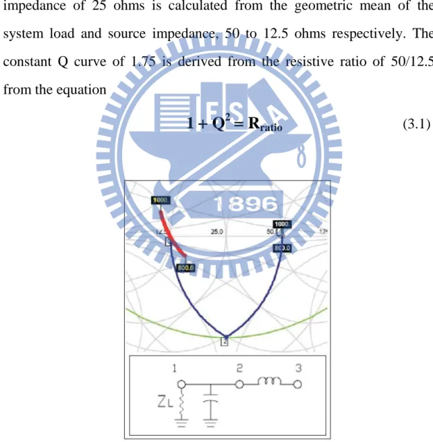
Shunt C and series L disperse a trajectory in smith chart with increasing frequency. In other words when using these matching elements in a low pass network, the higher frequencies will rotate and transform more than the lower frequencies, which spreads the trajectory relative to frequency in a clockwise direction. In Figure 3.4, a two-element low pass network is charted on a Z0 = 25 normalized Smith Chart. The normalized
impedance of 25 ohms is calculated from the geometric mean of the system load and source impedance, 50 to 12.5 ohms respectively. The constant Q curve of 1.75 is derived from the resistive ratio of 50/12.5 from the equation
1
Q
2
R
ratio (3.1)Figure 3.4 Z0=25, Q=1.75; node1-node2 shunt C=6.1pF;
node1-node2 series L=3.8nH; red line marks the trajectory dispersing ranging from 800MHz to 1000MHz
On the other hand, high-pass matching networks consisting of shunt inductors and series capacitors will transform the lower frequencies more than the higher frequencies. In Figure 3.5, a two-element high pass L-network transformation from 50 to 12.5 ohms is demonstrated on a 25-ohm normalized Smith Chart. It is easy to see that the trajectory , ranging from 800MHz to 1000MHz, of lower frequencies dispersing more than the higher ones.
Figure 3.5 Z0=25, Q=1.75; node1-node2 shunt L=5.1nH;
node1-node2 series C=8.2pF; red line marks the trajectory dispersing ranging from 800MHz to 1000MHz
Unlike a low-pass L-network, the higher frequencies are transformed less than the lower frequencies. If the low-pass trajectory of Figure 3.4 were overlaid onto Figure 3.5, the two trajectories would form the letter X. Exploiting this relationship by combining these dispersion
effects can leverage a broad band transformation. A broad band band-pass network is illustrated in Figure 3.6, a 50 (node1) to 3 (node5) ohm transformation. With the Smith Chart normalized to the geometric mean, it is easy to see that low pass nodes 1-2-3 are symmetrical in Q to the high pass nodes 3-4-5. Combining these two networks’ halves folds and compresses the trajectory into a condensed 3-ohm driving point load.
Figure 3.6 50 to 3-ohm transformation; Z0 = 12.5, Q = 1.75; node1-node2 Shunt C
= 6.10pF; node2-node3 Series L = 3.85 nH; node3-node4 Shunt L = 1.32 nH; node4-node5 Series C = 32.3 pF.
Compare to the simple two low pass L-network, as depicted in Figure 3.4 and Figure 3.5, the combination of Low-Pass and High-Pass L-Network obviously compresses the trajectory around node5 and thus broadening the bandwidth, shown in Figure 3.6.
3.3 Multiple-Q Method (Chebyshev broad-banding technique)
As a rule in broad band transformations, maintaining a lower Q (quality factor) curve for a given transformation by increasing the number of n-sections will yield a higher bandwidth. However, there is the limitation that using more than a four-section matching network will not yield greater bandwidth. To further extend the bandwidth, one of the effective ways is the multiple-Q method, also called Chebyshev broad-banding technique.
With the complexity of the multiple Q curve network, deriving a design from a Smith Chart alone would not be an intuitive process. Tables 3.1 and Tables 3.2 were derived by optimization with an ADS simulator utilizing a gradient optimizer.
Table 3.1 Q curves, 2-section network, per transformation ratio. The Q curves are numbered from the outer most Q1 towards the inner Q3. Q1 Q2 Q3 Trans. Ratio 0.72 0.71 0.61 1.67 0.82 0.80 0.62 2.00 1.27 1.22 0.58 5.00 1.63 1.51 0.50 10.00 1.96 1.71 0.45 16.67 2.19 1.91 0.42 25.00 2.39 2.01 0.38 33.30 2.72 2.15 0.35 50.00 3.30 2.53 0.29 100.00
Table 3.2 Q curves, 3-section network, per resistive transformation ratio. The Q curves are numbered from the outer most Q1 towards the inner Q3. Q1 Q2 Q3 Trans. Ratio 0.92 0.60 0.65 1.67 1.37 0.90 0.61 5.00 1.53 1.00 0.60 7.14 1.68 1.08 0.58 10.00 1.89 1.21 0.53 16.67 2.06 1.32 0.50 25.00 2.20 1.41 0.49 33.33 2.41 1.52 0.45 50.00 2.57 1.61 0.44 66.67 2.80 1.74 0.41 100.00
As illustrated in Figure 3.7, the transformation is mostly symmetrical with two Q curves, an outer curve (Q1 green) and an inner curve (Q3 magenta). However, node 5 falls at a higher impedance than the 3-ohm target in order to center the fish shaped trajectory at Z = 3 + j0 and so therefore a third Q curve (Q2, cyan) is defined at node 4.
Figure 3.7 Z0 = 12.3, SWR = 1.12 @ ZS = 3; N1-2 Shunt C = 6.9 pF; N2-3 Series
In Figure 3.8, there is a three-section transformation, the trajectory fits into a 3-ohm 1.01 SWR circle. Three Q curves are adequate for defining the three section network since the trajectory is small and circular in shape, unlike in Figure 3.7, here no impedance offset is needed at node 7.
Figure 3.8 Z0 = 12.2, SWR = 1.01 @ ZS = 3; N1-2 Shunt C = 4.30 pF, N2-3 Series
L = 6.22 nH; N3-4 Shunt C = 16.57 pF, N4-5 Series L = 2.42 nH; N5-6 Shunt C = 42.05 pF, N6-7 Series L =0.63 nH.
As mentioned above, Table 3.2 was derived from optimization. Here Q curves are provided for resistive transformation ratios of 1.67:1 (50 ohms to 30 ohms) to 100:1 (50 ohms to 0.5 ohms).
3.4 Dummy bias technique
This broadband technique is suitable for implementing in the gain block or the PA driver and has shown the excellent gain flatness.
Figure 3.9 Circuit diagram of dummy bias
This technique use smaller RF choke (L) and much larger bias resistor (R), hence causing more power consumption.
3.5 Bridged-T network
To deduce the Bridged-T network, an evolution view of circuit analysis is present. Starting from a simple L type LC low pass filter example shown in Figure 3.10, the 3dB bandwidth is about 1.35GHz.
Figure 3.10 A simple L type LC low pass filter
To extend the 3dB bandwidth, one more inductor is added and formed a T type low pass filter, the 3dB bandwidth extended to about 1.46GHz.
Based on the T type low pass filter, a capacitor is added between two terminators, after some adjusting, this capacitor significantly increased the 3dB bandwidth. This might be due to the zero included because of the new bridged capacitor.
Figure 3.12 A T type LC low pass filter added a bridged capacitor
The following will describe the use of the bridged-T input matching network that absorbs the FET input capacitance into a simple filter network to provide simultaneous gain flatness, good input return loss [9]. The bridged-T input matching network is a second-order “all-pass” network shown in Figure 3.13. In Figure 3.14, it shows a simplified linear FET model.
Figure 3.13 The prototype of the bridged-T matching networks
Neglecting Ri, Cds, and taking into account Miller effect, we
obtain the further simplified FET model of Figure 3.15, where Cin, is the
equivalent input capacitance and RL is the load impedance presented to
the FET stage.
Considering the circuit shown from Figure 3.13 to Figure 3.15, this bridged-T is a second-order all-pass network if L = Rs
2
Cgs/2,
C1=Cgs/4, R=Rs, [9]. When Ri >0 the network no longer is of the standard
all-pass form but L, C1 and R can still be chosen such that the generator sees a pure resistive at all frequencies. The design equations for this condition are [10]
R = Rs (3.2)
L = R/ωc (3.3)
C1 = 1/2ωcR (3.4)
Figure 3.14 Simplified FET linear model
Figure 3.15 Further simplified FET model with equivalent input capacitance
Combining Figure 3.15 with Figure 3.13 and using Cin, as C2 and
C as C1, we obtain the all-pass matching network of Figure 3.16. Arranging L and C and let the generator seeing a pure resistive R, this network provides a broad band resistive match as well as gain equalization up to the frequency of resonance, ωc. Although the all-pass
network itself has a flat amplitude response with no real cutoff frequency, the voltage across Cin (or C2) does decrease after ωc.
Figure 3.16 Bridged-T network with simplified FET model
The voltage (Vin) directly corresponds to the linear gain of the
FET stage, since this is the control voltage for the voltage controlled current source in the FET model. For a given Vin, ωc can be increased by
reducing R.
Comparing with prior broad band PA design methods, the Bridged-T input matching network is the most suitable method for our specs mainly due to the low Q characteristic.
Table 3.3 Comparison of Broad Band PA Design Method
Broad band PA Design Method Comparison
\ Balanced PA Distributed PA Bridged-T input matching Pros flat gain
good VSWR
large bandwidth flat gain
compact size, low pass (Q) flat gain
Cons coupler bandwidth issue low gain, low PAE,
Chapter 4
Practical Broad Band PA Design
The major task of this thesis is to design and implement an extremely broad band RF high power amplifier with a GaN HEMT unmatched transistor. A NITRONEX product “NPTB00004” [11] is chosen because of cost effectiveness and non-linear model availability. For a research-driven purpose, this device is suitable for the school lab to study or verify the circuit architecture since its package is SOIC-8, which is easy to solder on the PCB. A completely design and verification procedures are present in the following sections.
4.1 GaN HEMT large-signal modeling introduction
Recently, most effort in PA design has been focused on GaAs pseudomorphic HEMTs (pHEMTs), Si LDMOSFETs, and GaN HEMTs. Models have been developed and adapted to these devices and share many common features because they are all field-effect structures. The focus of this section is to introduce the development of GaN HEMT models.
Here present one possible solution to the modeling applied to the GaN HEMT while acknowledging that there are many other viable solutions. There are two general approaches to HEMT (or other active device) modeling. One is table-based, the best known of which has been developed by Root [12]. The table data can either be measured or
simulated using 2-D physical simulators. A more recent version of this approach is the new x-parameter model formulation, which is based on significant small- and large-signal measurements [13]. This approach can be very accurate, but requires intensive measurement resources. To improve accuracy, the entire simulation space must be mapped using both large- and small-signal measurements including load–pull and linearity.
It is certainly desirable to have the largest possible measurement database from which to extract and verify any model, but these measurements can be time consuming and expensive. A properly formulated model based on physical equations allows a reduction in required measurements without a significant loss in accuracy. The second approach involves the description of the active device by closed-form physical equations, the parameters of which can be extracted from measured data. This is the approach chosen to support the NITRONEX device model used in this thesis. The model described here uses various formulations, combined in such a way as to allow parameter extraction using a minimal set of measurements. A well-known application is found in Angelov (or Chalmers) model [14].
4.2 Bridged-T broad band design with large-signal model
In this thesis, NITRONEX GaN HEMT transistor NPTB00004 is used to design the Bridged-T network extremely broad band power amplifier. The vendor provides the large-signal model, a kind of Angelov model, executed in non-linear simulation, generating results such like compressed output power, harmonics, efficiency and linearity predicting.
43
4.2.1 Bias consideration
The goal of this thesis is to optimize to output power, therefore, the bias will be set to achieve max output power, rather than linearity. Based on the datasheet [11], the drain-source voltage Vds should be set at 28V, and the quiescent gate-source voltage, Vgsq, optimized for CW power and efficiency, should be regulated so as to get the quiescent drain current around 50mA.
Figure 4.1 ADS Schematic of bias sweeping
Figure 4.2 Result of bias sweeping
m1 VDS= IDS.i=0.053 VGS=-1.600000 28.000 10 20 30 40 50 0 60 50 100 150 200 0 250 VGS=-1.800 VGS=-1.700 VGS=-1.600 VGS=-1.500 VGS=-1.400 VGS=-1.300 VGS=-1.200 VGS=-1.100 VGS=-1.000 VDS ID S .i , m A m1 m1 VDS= IDS.i=0.053 VGS=-1.600000 28.000
By the simulation data shown in Figure 4.2, the quiescent gate-source voltage, Vgsq, getting around 50mA quiescent drain current at Vds 28V is about -1.6V. Under such bias condition, the PA will operate close to class-AB mode.
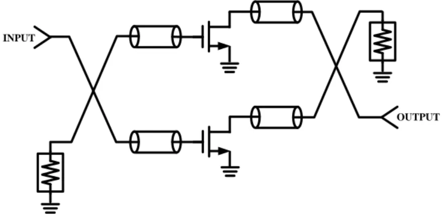
4.2.2 PA architecture
Intending to design an extremely broad band PA of operation frequency ranging from several tenth of MHz up to GHz, the most suitable input matching network architecture is the Bridged-T network, which is mentioned in 3.5 of Chapter 3. To enhance the gain flatness, the resistive feedback from the drain to the gate is also implemented in this design. Considering to the easy implementation and adjustability, a structure of LC sections (several pieces of microstrip section following grounded capacitor) is carried out as the output matching network.
VDD Vg INPUT OUTPUT OMN IMN LC Sections Bridged-T Network
4.2.3 PCB layout
A four layer PCB with 50 Ω grounded-CPW line was fabricated with FR-4, and soldered manually. The ground through-holes (via) are specifically arranged for minimize the grounding parasitic effect and enhance the heat transportation. The two screw holes fit the precise location of the heat sink used in this case. To deserve to be mentioned, the grounded-CPW line is draw with mini-meter rule nearby, which is convenient to accurately locate the parallel grounded capacitors.
Figure 4.4 PCB layout of the Bridged-T network extremely broad band PA
4.2.4 Non-linear simulation with large-signal model
After settling down the Bridged-T network, the non-linear simulation can be executed to get the PA load impedance with good broad band performance. A topology of three LC sections was adopted to become the PA output matching network due to easy design and simple implement. Tedious iteration between input and output matching adjustment made the simulation result contenting.
Figure 4.6 ADS Schematic of the Bridged-T network extremely broad band PA
By means of ADS non-linear simulation template, some non-linear characteristics of the power amplifier, suck like compression output power or harmonics, can be extracted from NPTB00004 Angelov model. By the way, the impedance of grounded-CPW line in the PCB layout (Figure 4.4) calculated by TXLINE calculator is 49.885 Ω, the microstrip with the same width calculated by TXLINE calculator is 49.0697 Ω. Therefore, the microstrip model is used in the simulation (Figure 4.6) for simplicity since the difference between them is trivial.
From Figure 4.7 to Figure 4.9, the design details of the bridged-T input matching network, resistive feedback and the output matching network are revealed.
Figure 4.7 The detail of the Bridged-T network in the ADS Schematic
Figure 4.9 The detail of the output matching network in the ADS Schematic
Figure 4.10 shows the gain flatness simulation data of this extremely broad band power amplifier. It drops after 1.3GHz and maintains excellent flatness before the rolling off. The transducer power gain was deduced from 3dB compression point and still be around 12dB in the pass band.
Table 4.1 ADS non-linear simulation data @P3dB
Transducer Power Gain Fundamental Frequency Fundamental Output Power dBm Second Harmonic dBc Third Harmonic dBc Fourth Harmonic dBc Fif th Harmonic dBc 100.0 M 200.0 M 300.0 M 400.0 M 500.0 M 600.0 M 700.0 M 800.0 M 900.0 M 1.000 G 1.100 G 1.200 G 1.300 G 1.400 G 1.500 G 37.04 37.21 37.39 37.51 37.51 37.36 37.21 37.34 37.50 37.58 37.44 37.18 36.81 36.15 35.18 11.58 11.60 11.56 11.56 11.56 11.58 11.64 11.74 11.87 11.98 12.05 12.04 11.88 11.52 10.95 -11.72 -12.38 -12.08 -11.66 -11.70 -12.09 -11.80 -11.95 -12.30 -12.97 -13.38 -12.72 -11.17 -9.293 -8.015 -14.99 -15.04 -15.13 -14.79 -14.61 -15.35 -17.40 -18.05 -18.08 -19.15 -20.67 -21.54 -19.42 -17.20 -17.04 -17.70 -17.25 -17.49 -19.43 -18.60 -16.88 -16.45 -17.53 -19.65 -19.62 -20.12 -23.19 -28.16 -32.00 -32.51 -25.55 -25.03 -24.22 -25.77 -28.05 -26.05 -23.66 -26.49 -29.72 -31.75 -33.17 -30.74 -42.44 -52.89 -58.87
Figure 4.10 The transducer power gain @ P3dB
Figure 4.11 shows 3dB compression output power and 2nd harmonic versus frequency simulation data of this broad band power amplifier. Data shows the output power being more than 37dBm till 1.2GHz, as well as 2nd harmonic kept around 11.5dBc before output power rolling off.
Figure 4.11 Fundamental output power, 2nd and 3rd harmonic vs. frequency@ P3dB
200. M 400. M 600. M 800. M 1. 00G 1.20G 1.40G 0. 000 1.60G 3 6 9 12 0 15 RFfreq
Transducer Power Gain, dB
2 0 0 .M 4 0 0 .M 6 0 0 .M 8 0 0 .M 1 .0 0 G 1 .2 0 G 1 .4 0 G 0 .0 0 0 1 .6 0 G 15 20 25 30 35 10 40 RFfreq S p e ct ru m [1 ] S p e ct ru m [2 ] S p e ct ru m [3 ]
4.3 Verification and measurement
The most essential task of all is to measure, verify as well as tune
the soldered “NPTB00004 Bridged-T Networkextremely broad band PA” PCB in this work. Both small and large signal measurement data are collected and put in order.
4.3.1 Bias measurement
The actual bias setting is a little different from the simulation.
VDD is still the same set at 28V. However, in order to get the quiescent drain current around 50mA, the gate voltage (Vg) must adjust to -1.4V, instead of the bias simulation result -1.6V.
Figure 4.12 The picture of NPTB00004 Bridged-T
Network extremely broad band PA PCB
4.3.2 Small signal measurement
As depicted in Figure 4.13, the small signal measurement data are
quite similar to the simulation data. Input return loss and output return loss match fairly well, only the gain of the measurement data is somewhat
larger than the simulation data in the pass band. It is observed that the gain roll off slightly after 1.2GHz, significantly rolling off after 1.4GHz.
Figure 4.13 S-parameter simulation and measurement data comparison
4.3.3 Environment setup for large signal measurement
Figure 4.14 shows the setup of NPTB00004 Bridged-T Network extremely broad band power amplifier large signal measurement. A Broad band PA driver made of Mitsubishi GaAs FET MGF0951P [15] is used to drive this extremely broad band power amplifier. A 50W 30dB attenuator is to protect the spectrum and avoiding extra non-linearity produced by the spectrum itself.
Figure 4.15 Picture of large signal measurement setup
4.3.4 Large signal measurement
The large signal measurement data describe in the following pages, which are measured under the environment setup depicted in 4.3.3 of this chapter. The measurement items include output power, 2nd harmonic, 3rd harmonic, gain and PAE. The measurement frequency ranges from 150MHz to 1.2GHz.
Figure 4.16 Large signal measurement data@ 150MHz
Figure 4.18 Large signal measurement data@ 600MHz
Figure 4.19 Large signal measurement data@ 900MHz
To summarize the miscellaneous measurement data to a more concise presentation, a chart in Figure 4.21 extracts the information showing up from Figure 4.16 to Figure 4.20.
Figure 4.21 Summary of all the large signal measurement @ Pin 27dBm
Table 4.2 Raw data of Figure 4.21
4.4 Result analysis and discussion
From Figure 4.21 and Table 4.2, a performance overview of the NPTB00004 Bridged-T Network extremely broad band power amplifier can be taken in at a glance. It shows that the output power can exceed 37dBm (except 150MHz) while input power as high as 27dBm in the pretty wide operation frequency range. Within the operation frequency ranging from 150MHz to 1200MHz, the maximum output power, driving by 27dBm input power, could be as high as 38.2dBm, while minimum
Freq. (MHz) Pin (dBm) Pout (dBm) Gain (dB) 2nd Harmonic (dBm) 2nd Harmonic (dBc) 3rd Harmonic (dBm) 3rd Harmonic (dBc) Id (mA) PAE (%) 150 27 36.55 9.55 27.06 -9.49 19.16 -17.39 370 43.62 300 27 37.72 10.72 25.08 -12.64 24.55 -13.17 420 50.30 600 27 38.2 11.2 25.65 -12.55 24.33 -13.87 450 52.44 900 27 37.3 10.3 26.65 -10.65 20.14 -17.16 420 45.67 1200 27 37.26 10.26 26.44 -10.82 5.27 -31.99 360 52.79
output power reaches 36.55dBm. Also under such driving condition and frequency range, PAE all exceeding 40%, 2nd harmonic being around -11dBc, 3rd harmonic ranging from -13.17dBc to -31.99dBc and the compressed gain is about 10dB.
Table 4.3 Achieved performances of this work @ Pin 27dBm
Categories Min Max
Frequency range (MHz) 150 1200 Gain (dB) 9.55 11.2 Output Power (dBm) 36.55 38.2 PAE (%) 43.62 52.79 2nd harmonic (dBc) -12.64 -9.49 3rd harmonic (dBc) -31.99 -13.17
Though the output power can exceed 37dBm, from Figure 4.10 to Figure 4.14, we can observe that non-linearity or compression imperceptibly begin at 22dBm or so, depending on the frequency. It is just as well to use in constant envelope modulation such like FSK or GMSK, which remains constant amplitude and the data is modulated using the phase of the carrier signal. Whereas in non-constant envelope modulation schemes like CDMA, the amplitude of the signal also carries some data information and hence it is important to maintain the exact shape of the signal without introducing any distortion through the power amplifier. Extremely linear power amplifiers are required for non-constant envelope modulation techniques, while the linearity can be traded-off for better efficiency in constant envelope modulation schemes.