Edge-coupled membrane terahertz photonic transmitters based
on metal–semiconductor–metal traveling-wave photodetectors
Jin-Wei Shi, Shi-Wei Chu, and Ming-Chun Tien
Graduate Institute of Electro-Optical Engineering, National Taiwan University, Taipei 10617, Taiwan, Republic of China
Chi-Kuang Suna)
Graduate Institute of Electro-Optical Engineering and Department of Electrical Engineering, National Taiwan University, Taipei 10617, Taiwan, Republic of China
Yi-Jen Chiu and John E. Bowers
Department of Electrical and Computer Engineering, University of California, Santa Barbara, Santa Barbara, California 93106-5050
共Received 19 August 2002; accepted 5 November 2002兲
Ultra-high-speed photodetectors and printed-circuit antennas construct photonic transmitters. In this letter, we demonstrate a terahertz 共THz兲 photonic transmitter: edge-coupled membrane photonic transmitters based on metal–semiconductor–metal traveling-wave photodetectors, which are fabricated with low-temperature-grown GaAs photoabsorption layers. With a membrane-based and edge-coupled structure, the demonstrated photonic transmitters can eliminate the requirement of Si lenses and attain an over 20 times higher optical-to-THz power conversion efficiency 2⫻10⫺4than vertical illuminated photonic transmitters with Si lenses at the same operation frequency. © 2002
American Institute of Physics. 关DOI: 10.1063/1.1533846兴
Photonic transmitters are composed of ultra-high-speed photodetectrs共PDs兲 and printed-circuit antennas.1Under op-tical excitations with high-repetition-rate共GHz–THz兲 mode-locked laser diodes2,3or heterodyne-mixed continuous-wave 共cw兲 laser diodes,4 photonic transmitters can radiate high-frequency electromagnetic waves. Low-temperature-grown 共LTG兲 GaAs-based photonic transmitters attract lots of atten-tions due to their ability to operate in the THz frequency regime共corresponding to 100–1000m optical wavelength兲, which lies beyond the capabilities of both solid-state lasers on the short-wavelength side and of electronic sources such as Gunn or IMPATT diodes5 on the long-wavelength side. Compared with other millimeter- or submillimeter-wave emission techniques such as Gunn diodes,5p-type Ge-based
or quantum-cascade THz lasers,6,7 and resonant tunneling diodes,8 photonic transmitters have the advantages of sim-plicity, compactness, wide tunability, and room-temperature operation capability. The demonstrated LTG-GaAs-based photonic transmitters have been applied in THz image sys-tems and THz spectrometers.9,10 There are two main trends in the advance of photonic transmitters:11,12 improving optical-to-THz power conversion efficiency and obtaining high radiation power. Achieving higher conversion efficiency plays a key role in the integration of photonic transmitter systems. High-conversion-efficiency photonic transmitters relieve the power burden imposed on excitation semiconduc-tor lasers. By utilizing the heterodyne mixing technique with cw lasers, the state-of-the-art LTG-GaAs-based vertical-illuminated photomixer with an optical resonant cavity and a resonant twin-dipole antenna structure demonstrated
conver-sion efficiencies around 3.3⫻10⫺5and 9⫻10⫺6at 850 GHz and 1.6 THz, respectively.12,13 Adopting high-conversion-efficiency edge-coupled ultra-high-speed photodetectors should further improve the bandwidth-efficiency product as
well as the conversion efficiency of photonic
transmitters.11,12 However, the previously demonstrated edge-coupled THz distributed photomixers exhibited much lower conversion efficiency than the vertical-illuminated photomixers.14
In this letter, we demonstrate a LTG-GaAs-based THz photonic transmitter, which is composed of an edge-coupled metal–semiconductor–metal 共MSM兲 traveling-wave photo-detector 共TWPD兲 共Refs. 15–17兲 and a co-planar-waveguide 共CPW兲 fed slot antenna.18 By utilizing a membrane antenna structure and taking advantage of the superior fully distrib-uted microwave guiding property in MSM TWPDs, high-optical-to-THz-power conversion efficiency (⬃2⫻10⫺4) can be achieved by testing the photonic transmitter under pulsed operation condition at a 1.6 THz frequency without using Si lenses.
The top view of the demonstrated device is shown in Fig. 1. We adopt a CPW fed slot antenna in our demonstrated device because it can generate higher power than the spiral antenna in the designed resonant frequency4and can be eas-ily integrated with the MSM TWPD, which has a CPW struc-ture to support the photoexcited microwave-guiding mode.15–17 A quarter-wavelength impedance transformer is placed between the CPW fed slot antenna and the MSM TWPD for impedance matching. This impedance matching stub is important for a maximum electrical power transfer from the TWPD to the antennas. The radio-frequency 共rf兲 isolation bias tee, which acts as an inductance,19 avoids the high-frequency ac current 共with a resonant frequency of the slot line antenna兲 leaking into the dc probe pad. Comparing a兲Author to whom correspondence should be addressed; electronic
mail: [email protected]
APPLIED PHYSICS LETTERS VOLUME 81, NUMBER 27 30 DECEMBER 2002
5108
our active photoabsorption region with that of the previous edge-coupled distributed photomixer,14the optical scattering loss between adjacent distributed active regions can be avoided with our demonstrated structure. Another advantage is that the electrical bandwidth of our fully distributed MSM TWPD will not be limited by the Bragg cutoff frequency.20 The detailed fabrication processes of our demonstrated de-vice are almost identical to that of the self-aligned MSM TWPDs and are given in Ref. 15. For most photomixers operating in millimeter- and submillimeter-wavelength re-gimes, Si lenses are required for improving the antenna ra-diation efficiency from substrates.21 However, this integra-tion will increase the cost of packaging. In addiintegra-tion, the long distance between the center 共where the antenna should be兲 and the edge共where the photodetector edge should be兲 of the available Si lens is also an obstacle for the edge-coupled input optical beam. In order to overcome this problem, we use a membrane structure in our demonstrated edge-coupled THz photonic transmitters. We removed the GaAs substrate and mounted the membrane of the fabricated device on a glass substrate, which has a much lower dielectric constant than the GaAs layer and can thus allow the radiation of THz energy into the substrate or free space more easily.21 This technique has been adopted in the packaging of ultra-high-speed photodetectors for mass production purposes.22 The geometric sizes of the measured devices are given in Table I, which has been used to simulate the frequency response of the S11parameter of this demonstrated structure.
23
The simu-lation results show a resonant frequency near 1.6 THz due to the resonant CPW fed slot antenna.
In order to measure the device performance, we used a mode-locked Ti:sapphire laser with a repetition rate of 82 MHz. By passing the broadband femtosecond optical pulses through e´talons, we can increase the repetition rate of the light source and trigger the photonic transmitters by coupling this high-repetition-rate light into the edge-coupled MSM TWPD. We used microscope cover glasses with double-sided silver coating as the e´talon filters. The thickness of the e´tal-ons determines the optical longitudinal mode spacing and repetition rate of the optical pulse train. Some mode-locked semiconductor lasers also use a similar principle to increase the repetition rate to the THz frequency regime by means of intracavity reflectors.2 The e´talons that we fabricated have four different resonant frequencies, which are 490 GHz, 670 GHz, 1.1 THz, and 1.6 THz. Take the Ti:sapphire spectrum after the 1.6 THz e´talon, for example, which is shown as an inset of Fig. 2, the free spectral range of this e´talon filter is found to be ⬃3.2 nm with a full width at half maximum
共FWHM兲 of the transmission peaks ⬃1.3 nm. The FWHM of the transmission peaks implies that the time domain FWHM of the generated optical pulse train envelope is around ⬃1 ps. We used two parabolic mirrors to collimate and focus the radiated THz pulse onto a liquid-helium-cooled Si bolometer for power measurement. We modulated the excitation optical beam with a mechanical chopper and connected the output electrical signal of the bolometer to a lock-in amplifier to improve the signal/noise ratio. The responsivity of the Si bolometer was calibrated with a blackbody radiation source.4,12 The THz beam propagation loss in air was also measured and calibrated by measuring the THz power as a function of distance. For example, the obtained propagation loss at 1.6 THz is about ⬃17.1 dB/m.
Figure 2 shows the normalized THz power radiated from the photonic transmitter at four different operation frequen-cies under the same operation condition. We excited the de-vice with the same optical average power under a fixed dc bias voltage. We can observe that under the 1.6 THz opera-tion condiopera-tion the demonstrated device exhibits the highest THz output power. This measurement result is consistent with the antenna simulation result,23 as discussed before. Figure 3 shows the measured bias-dependent output power FIG. 1. Schematic diagram共top view兲 of the demonstrated THz photonic
transmitter.
FIG. 2. Measured THz power at four different operation frequencies. Inset shows the measured optical spectrum after a 1.6 THz e´talon filter. TABLE I. Geometric sizes of the demonstrated THz photonic transmitter.
Geometric size Center strip and air gap widths in
the MSM TWPD active region
2m/0.3m
MSM TWPD length 20m
Gap width of CPW fed slot line antenna
2m
Total length of CPW fed slot line antenna
70m
Center strip and air gap widths of the impedance transformer
10m/7m
Impedance transformer length 35m
Width and length of rf isolation bias tee fingers
2m/35m
Total thickness of GaAs-based epilayer and glass substrate
5m/1 mm
Metal共Ti/Au兲 thickness 1m
5109
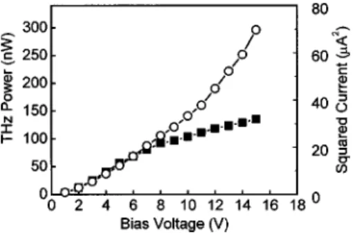
共solid square兲 at the 1.6 THz frequency after considering the propagation loss under a fixed optical power excitation共0.66 mW兲. High conversion efficiency of ⬃2⫻10⫺4between op-tical excitation power 共before coupling into the MSM TWPD兲 and collected THz radiation power are achieved at a 15 V dc bias voltage. The obtained 135 nW average THz power corresponds to a peak THz power of 1.6 mW. In our measurement setup, we collected only the radiated power from the glass substrate side, thus even higher output power and conversion efficiencies can be expected if we can also collect the THz radiation from the free-space side. We ne-glected the THz power contribution from high harmonic fre-quencies 共3.2 THz, 4.8 THz, etc.兲 because of the electrical bandwidth limitation in MSM TWPD共less than 1 THz兲 and the bandwidth共100 GHz–3 THz兲 of a THz filter inside the Si bolometer. The obtained conversion efficiency is much higher than the previously reported values12,13 and can be attributed to the improved bandwidth-efficiency perfor-mances of the adopted LTG-GaAs-based MSM TWPDs than the vertical-illuminated LTG-GaAs based PDs.15 The mea-sured THz power from photomixers exhibits a near-quadric dependency on the applied bias voltage and excitation opti-cal power,12 thus higher conversion efficiency along with higher radiated power than the values shown in Fig. 3 can be expected with increased optical pumping power and dc bias voltage. The above demonstrated maximum radiation power and conversion efficiency of this device is limited by the damage threshold of the e´talon filters, instead of the band-width degradation or thermal heating problems of this device.12 We square the measured bias-dependent photocur-rents 共open circles, Fig. 3兲 and compare them to the bias-dependent THz output power in Fig. 3. It can be observed that the radiated THz power is proportional to the squared photocurrents when the bias voltage is below 7 V. However, under high dc bias voltages 共8–15 V兲, the radiated THz power starts to saturate. We attribute this phenomenon to the lifetime increasing effect in LTG-GaAs-based PDs under high bias voltages.12,16Carrier lifetime increase implies elec-trical bandwidth degradation and output power degradation in the THz frequency regime.
In conclusion, by using the edge-coupled MSM TWPD with superior microwave guiding properties, we demonstrate a membrane THz photonic transmitter without Si lenses and attain a high-optical-to-THz power conversion efficiency (2
⫻10⫺4) under a pulsed operation condition. The maximum THz radiation power and the optical-to-THz conversion effi-ciency were limited by the maximum allowable optical power transmitted after the e´talon filters. The edge-coupled structure and high-conversion-efficiency characteristic of our demonstrated devices are suitable for monolithic integration with a mode-locked semiconductor laser with high repetition rate or a two-wavelength cw diode laser. The integrated de-vice can act as a compact, all-solid-state, and tunable THz radiation source.
This work is sponsored by the National Science Council of Taiwan, under NSC91-2215-E-002-021 and NSC91-2112-M-002-050, and partially sponsored by Institute of Applied Science and Engineering Reserach, Academia Sinica, Tai-wan.
1T. Nagatsuma, M. Shinagawa, N. Sahri, A. Sasaki, Y. Royter, and A.
Hirata, IEEE Trans. Microwave Theory Tech. 49, 1831共2001兲.
2
D. A. Yanson, M. W. Street, S. D. McDougall, I. G. Thayne, J. H. Marsh, and E. A. Avrutin, Proceedings of the 2001 International Topical Meeting on Microwave Photonics Technical Digest共2002兲, p. 25.
3S. Arahira, Y. Matsui, and Y. Ogawa, IEEE J. Quantum Electron. 32, 1211 共1996兲.
4S. Verghese, K. A. McIntosh, and E. R. Brown, IEEE Trans. Microwave
Theory Tech. 45, 1301共1997兲.
5H. Eisele, A. Rydberg, and G. I. Haddad, IEEE Trans. Microwave Theory
Tech. 48, 626共2000兲.
6
Yu. P. Gousev, I. V. Altukhov, K. A. Korolev, V. P. Sinis, M. S. Kagan, E. E. Haller, M. A. Odnoblyudov, I. N. Yassievich, and K.-A. Chao, Appl. Phys. Lett. 75, 757共1999兲.
7R. Kohler, A. Tredicucci, F. Beltram, H. E. Beere, E. H. Linfield, A. G.
Davies, D. A. Ritchie, R. C. Iotti, and F. Rossi, Proceedings of the Con-ference on Lasers and Electro-Optics共CLEO兲, OSA, postdeadline papers, CPDC 12-1共2002兲.
8M. Reddy, S. C. Martin, A. C. Molnar, R. E. Muller, R. P. Smith, P. H.
Siegel, M. J. Mondry, M. J. W. Rodwell, H. Kroemer, and S. J. Allen, Jr., IEEE Electron Device Lett. 18, 218共1997兲.
9K. J. Siebert, H. Quast, R. Leonhardt, T. Loffler, M. Thomson, and S.
Czasch, Appl. Phys. Lett. 80, 3003共2002兲.
10C. Pin, G. A. Blake, M. C. Gaidis, E. R. Brown, K. A. McIntosh, S. Y.
Chou, M. I. Nathan, and F. Williamson, Appl. Phys. Lett. 71, 1601共1997兲.
11
K. Kato, IEEE Trans. Microwave Theory Tech. 47, 1265共1999兲.
12A. W. Jackson, Ph.D. thesis, University of California at Santa Barbara 共1999兲.
13S. M. Duffy, S. Verghese, K. A. McIntosh, A. Jackson, A. C. Gossard, and
S. Matsuura, IEEE Trans. Microwave Theory Tech. 49, 1032共2001兲.
14E. K. Duerr, K. A. McIntosh, S. Verghese, Proceedings of the Conference
on Lasers and Electro-Optics共CLEO兲, OSA Technical Digest 共2000兲, p. 382.
15
J.-W. Shi, K. G. Gan, Y. J. Chiu, Y.-H. Chen, C.-K. Sun, Y. J. Yang, and J. E. Bowers, IEEE Photonics Technol. Lett. 13, 623共2001兲.
16K. G. Gan, J.-W. Shi, Y.-H. Chen, C.-K. Sun, Y. J. Chiu, and J. E. Bowers,
Appl. Phys. Lett. 80, 4054共2002兲.
17J.-W. Shi, K. G. Gan, Y.-H. Chen, C.-K. Sun, Y. J. Chiu, and J. E. Bowers,
IEEE Photonics Technol. Lett. 14, 1587共2002兲.
18B. K. Kormanyos, W. Harokopus, Jr., Linda P. B. Katehi, and G. M.
Rebeiz, IEEE Trans. Microwave Theory Tech. 42, 541共1994兲.
19K. C. Gupta, R. Garg, I. Bahl, and P. Bhartia, Microstrip Lines and Slot-lines,共Artech House, Boston, MA, 1996兲.
20
T. T. Wong, Fundamental of Distributed Amplification 共Artech House, Boston, MA, 1993兲.
21D. B. Rutledge, D. P. Neikirk, and D. P. Kasilingam, Proceedings of the
Conference on Infrared and Millimeter Waves共1983兲, Vol. 10.
22
Y. Royter, T. Furuta, S. Kodama, N. Sahri, T. Nagatsuma, and T. Ishibashi, IEEE Electron Device Lett. 21, 158共2000兲.
23Zeland Software, Inc. IE3D, Taipei, Taiwan. FIG. 3. Measured THz output power共solid square兲 and squared
photocur-rents共open circle兲 vs bias voltage under a fixed optical excitation power of 0.66 mW.