i
國 立 交 通 大 學
應用化學研究所
博 士 論 文
新穎四元硫鉍鉛礦型結構硒化物的合成與特性鑑定
Synthesis and Characterization of New Lillianite-type Quaternary
Homologous Series of Selenides
研 究 生:陳奎伯
指導教授:李積琛 博士
中 華 民 國 九 十 九 年 五 月
新穎四元硫鉍鉛礦型結構硒化物的合成與特性鑑定
Synthesis and Characterization of New Lillianite-type Quaternary
Homologous Series of Selenides
研 究 生:陳奎伯
Student:Kuei-Bo Chen
指導教授:李積琛
Advisor:Chi-Shen Lee
國 立 交 通 大 學
應 用 化 學 系
博 士 論 文
A ThesisSubmitted to Department of Applied Chemistry College of Science
National Chiao Tung University in partial Fulfillment of the Requirements
for the Degree of Doctor of Philosophy
in
Applied Chemistry
iii
Contents
PageChinese Abstract vi
English Abstract viii
Acknowledgments x
List of Tables xi
List of Figures xiv
Chapter 1 Introduction 1
1.1. Thermoelectric materials 1
1.2. Homologous series 9
1.3 Motivation and goal of this thesis 12
Chapter 2
Experimental and Theoretical Studies of Sn3-δPbδBi2Se6 (δ = 0.0 – 0.7)
14
2.1 Experiments 15
2.1.1 Synthesis 15
2.1.2 Single-crystal X-ray Diffraction (XRD) 16
2.1.3 Characterization 25
2.1.4 Physical Property Measurements 25
2.1.5 Theoretical Calculations 26
2.2 Results and Discussion 27
2.2.1 Crystal Structure 27 2.2.2 Electronic Structure 31 2.2.3 Physical Properties 34 2.2.4 Thermoanalysis 35 2.3 Conclusions 37 Chapter 3
Experimental and Theoretical Studies of (PbxSn1-x)6Bi2Se9 (x= 0 – 4.36)
38
3.1 Experiments 39
3.1.1 Synthesis 39
3.1.2 Single-crystal X-ray diffraction (XRD) 39
3.1.4 Physical Property Measurements 43 3.1.5 Calculation of the Electronic Structure 43
3.2 Results and Discussion 44
3.2.1 Synthesis and Structure Analysis 44
3.2.2 Crystal Structure 48
3.2.3 Electronic Structure 50
3.2.4 Physical Properties 52
3.2.5 Thermoanalysis 54
3.3 Conclusions 55
Chapter 4 Synthesis and Characterization of Quaternary Selenides Sn2Pb5Bi4Se13 and Sn8.65Pb0.35Bi4Se15 56 4.1 Experiments 57 4.1.1 Synthesis 57 (a) Sn2Pb5Bi4Se13 57 (b) Sn8.65Pb0.35Bi4Se15 58
4.1.2 Single-crystal X-ray diffraction (XRD) 60
(a) Sn2Pb5Bi4Se13 60
(b) Sn8.65Pb0.35Bi4Se15 61
4.1.3 Characterization 64
4.1.4 Calculation of the Electronic Structure 65
4.1.5 Physical Property Measurements 65
4.2 Results and Discussion 66
4.2.1 Description of the structure 66
(a) Sn2Pb5Bi4Se13 66 (b) Sn8.65Pb0.35Bi4Se15 67 4.2.2 Electronic Structure 69 (a) Sn2Pb5Bi4Se13 69 (b) Sn8.65Pb0.35Bi4Se15 70 4.2.3 Physical Properties 73 4.2.3 Thermoanalysis 73 4.3 Conclusions 76
v Pb12.92Sb2.08Bi2Se19
5.1 Experiments 78
5.1.1 Synthesis 78
5.1.2 Single-crystal X-ray diffraction (XRD) 79
5.1.3 Characterization 83
5.1.4 Physical Property Measurements 84
5.1.5Calculation of the Electronic Structure 84
5.2 Results and Discussion 85
5.2.1 Crystal structure 85
5.2.2 Electronic Structure 87
5.2.3 Physical Properties 88
5.2.4 Thermoanalyses 89
5.3 Conclusions 90
Chapter 6 Synthesis and Characterization of Quaternary Selenides Sn4Bi10Se19 and Sn8.5Pb1.5Bi18Se37
91 Synthesis 92
Single-crystal X-ray diffraction (XRD) 93
Structure description 98
Chapter 7 Conclusions 99
References 101
新穎四元硫鉍鉛礦型結構硒化物的合成與特性鑑定
學生: 陳奎伯 指導教授: 李積琛 博士
國立交通大學應用化學研究所
摘要
我們使用固態燒合成四元鉍鉛礦型結構硒化物,藉由單晶繞射解析並研究其晶體結 構。利用能帶計算與物理性質量測來證明這類化合物均具有半導體性質。 在第一部份中合成出具有相寬的四元化合物Sn3-xPbxBi2Se6 (x = 0 - 0.7),此結構為Pnma (No. 62)空間群之斜方晶系,與礦物中的硫鉍鉛礦 Pb3Bi2S6(Lillinite)的結構相似。
差異在於接近tropochemical cell-twinning 面上之原子並非呈現鏡面對稱,而是滑動對稱。 單晶結果顯示,當鉛的含量增加時,原子逐漸往tropochemical cell-twinning 面上移動, 由理論計算出來的結果顯示,當不是放在tropochemical cell-twinning 面上時具有較強的 鍵結能與較低的結構總能量。此一結果會影響解晶時所選擇空間群的正確性。 第二部份為具有相寬的四元化合物PbxSn6-xBi2Se9 (x=0 – 4) ,此結構為空間群 Cmcm (No. 63)之斜方晶系,與 Pb6Bi2S9結構相同。此化合物為NaCl-(311)層狀結構所組成,標 示為L(7, 7),表示攣晶面兩邊各由七層八面體的寬度沿著[010]的方向組成。 第三部份中,Sn2Pb5Bi4Se13 與 Sn8.65Pb0.35Bi4Se15為不具有相寬之四元化合物,其空 間群均為C2/m (No.12)斜方晶系。兩者結構上均具有硫鉍鉛礦系列的特性,於同系列的 分類法標示分別為L(4, 5)與 L (4, 7) 由導電度與理論計算的結果證實具有狹窄能隙之半 導體,Sn2Pb5Bi4Se13 和 Sn8.65Pb0.35Bi4Se15的Seebeck 係數分別為-80 和 178 (μV/K)。 最後,Pb13Sb2.08Bi1.92Se19為新結構的化合物,屬於C2/m (No. 12)空間群之單斜晶系,
vii 晶胞常數為a = 14.127(3) Å, b = 4.2625(8) Å, c = 34.477(6) Å, β = 96.329(4)°,最後所得之 R 值為 R1/wR2/GOF = 0.0351/0.0822/1.045, Pb13Sb2.08Bi1.92Se19有NaCl-(311)層狀結構,於 同系列的分類法標示為L(7, 8)。並經由理論計算與導電度、Seebeck 係數的量測,證實 為具有半導體性質的材料。
Synthesis and Characterization of New Lillianite-type Quaternary
Homologous Series of Selenides
Student: Kuei-Bo Chen Advisor: Dr. Chi-Shen Lee
Department of Applied Chemistry
National Chiao Tung University
Abstract
In this dissertation, all selenide compounds were synthesized by solid state method. These structures were determined and investigated with X-ray diffraction of single crystals. Calculations of the density of states, measurements of Seebeck coefficient and electrical conductivity confirm that these compounds are p- or n-type semiconductors with a narrow band gaps.
Firstly, New ternary and quaternary chalcogenides Sn3-xPbxBi2Se6 (x = 0 - 0.7) were
synthesized and crystallize in the orthorhombic space group Pnma (No. 62). The structure for these compounds is related to Pb3Bi2S6 with an atomic position near the cell-twining plane
with lillianite homologous series L(4, 4). The ternary phase contains partially occupied Sn site and a quaternary system exhibits a phase width in the range of 0 ≦ x ≦ 0.7. Single-crystal structure analysis indicates that there is a correlation between the Pb composition and position shift of M5 site from the cell-twining plane. Band structure calculations confirmed that the structure is more stable when the position of M5 site is shifted away the cell-twining plane.
ix
orthorhombic space group Cmcm (No. 62) and isostructural to the mineral heyrovskyite, Pb6Bi2S9. The PbxSn6-xBi2Se9 features a three-dimensional framework containing slabs of
NaCl-(311) type with lillianite homologous series L(7, 7) . PbxSn6-xBi2Se9 exhibits identical
layers of 7 octahedra wide slabs and each slab is composed of fused rectangular [M12Se12] rod
units that are expanded along direction [010].
In the third section, quaternary selenides Sn2Pb5Bi4Se13 and Sn8.65Pb0.35Bi4Se15 were
synthesized and crystallize in monoclinic space group C2/m (No.12). These compounds exhibit tropochemical cell-twinning of NaCl-type structures with lillianite homologous series L(4, 5) and L(4, 7) for Sn2Pb5Bi4Se13 andSn8.65Pb0.35Bi4Se15, respectively. Measurements of
electrical conductivity indicate that these materials are semiconductors with narrow band gaps; Sn2Pb5Bi4Se13 is n-type, whereas Sn8.65Pb0.35Bi4Se15 is a p-type semiconductor with Seebeck
coefficients -80(5) and 178(7) μV/K at 300K, respectively.
Finally, quaternary chalcogenides Pb13Sb2.08Bi1.92Se19 was synthesized and crystallize in
monoclinic space group C2/m (No.12), with lattice parameters of Pb13Sb2.08Bi1.92Se19: a =
14.127(3) Å, b =4.2625(8) Å, c = 34.477(6) Å, β= 96.329(4)°, R1/wR2 = 0.0351/0.0822 and
GOF = 1.045. These structures reveal novel structure type. Pb13Sb2.08Bi1.92Se19 features a
three-dimensional framework containing alternate layers of 7 and 8 octahedra wide slabs of NaCl-(311) type with lillianite homologous series L(7, 8). The semiconductor properties are confirmed with electronic calculations, Seebeck coefficient and electrical conductivity measurements.
Acknowledgments
漫長的碩博八年時間一轉眼就結束,這段時間內經歷了很多,也學習
了很多。能夠完成這本博士論文,首先要感謝的就是我的指導老師 李積琛
教授的諄諄教誨,讓我對科學研究與人生的價值有了更進一步的瞭解。此
外也要感謝百忙中撥空參加口試的裘性天 教授、陳登銘 教授、許火順 教
授,以及中正大學的廖儒修 教授,對於論文內容提供了許多寶貴的意見。
在實驗室裡,最感謝明芳同學,在我需要的任何時間、事情,不論是
生活上、課業上,都毫不猶豫的給予援手,如果沒有你的幫忙,能不能畢
業應該還是個大問題。已經畢了業的翊媚、靜宜、芳卿、冠程、大毛、偉
印、香蕉、翔翔,一起度過研究生活的時光不曾忘記。實驗室的博班成員
呆呆、阿明、郝哥、文亨,感謝你們在實驗上的幫助,實驗室的未來就靠
你們了。另外,佳芬、家瑜、俊明、俊超、蝌蚪、書維等學弟妹,活潑的
個性使實驗室充滿了歡樂的氣氛。好友亞玄、韋達、盈真,因為我的固執
堅持害你們吃不少苦,謝謝你們對我這麼大的信任。
當然不忘感謝我的家人無條件的為我付出,不管在經濟上還是精神上,
對我來說都是相當重要的,尤其是母親對我的支持已不是用筆墨所能表達
我對她的感謝。
最後,這本論文要獻給天國的子怡,我有努力在執行當年的承諾。 我
深信,帶著我對大家的感謝及大家對我的支持,可以讓我更堅強的面對未
來的種種挑戰。
xi
List of Tables
Page Chapter 1
Table 1.1 The sulfosalts with known structures of lillianite family 11
Chapter 2
Table 2.1 Crystallographic Data for Sn2.67Bi2.26Se6 and Sn3-δPbδBi2Se6. (δ =
0, 0.1, 0.3, 0.5, 0.7)
21 Table 2.2 Selected Interatomic Distances in Å for Sn3-δPbδBi2Se6 22 Table 2.3a Fractional Atomic Coordinates and Equivalent Isotropic Atomic
Displacement Parameters (Ueq) in 10-3 (Å2) and Site Occupancies for
Sn3Bi2Se6
22
Table 2.3b Fractional Atomic Coordinates and Equivalent Isotropic Atomic Displacement Parameters (Ueq) in 10-3 (Å2) and Site Occupancies for
Sn3-δPbδBi2Se6. (δ = 0.1)
23
Table 2.3c Fractional Atomic Coordinates and Equivalent Isotropic Atomic Displacement Parameters (Ueq) in 10-3 (Å2) and Site Occupancies for
Sn3-δPbδBi2Se6. (δ = 0.3)
23
Table 2.3d Fractional Atomic Coordinates and Equivalent Isotropic Atomic Displacement Parameters (Ueq) in 10-3 (Å2) and Site Occupancies for
Sn3-δPbδBi2Se6. (δ = 0.5)
24
Table 2.3e Fractional Atomic Coordinates and Equivalent Isotropic Atomic Displacement Parameters (Ueq) in 10-3 (Å2) and Site Occupancies for
Sn3-δPbδBi2Se6. (δ = 0.7)
24
Table 2.4 Three models with varied assignments of metal sites for LMTO calculations
26 Table 2.5 Bond valence for Sn3-δPbδBi2Se6 (δ = 0 – 0.7) 30
Chapter 3
Table 3.1 Crystallographic Data for PbxSn6-xBi2Se9 (x=0, 1.78, 4.36) 40 Table 3.2a Fractional Atomic Coordinates and Equivalent Isotropic Atomic
Displacement Parameters (Ueq / 10-3 Å2) and Site Occupancies for Sn6Bi2Se9
Table 3.2b Fractional Atomic Coordinates and Equivalent Isotropic Atomic Displacement Parameters (Ueq / 10-3 Å2) and Site Occupancies for
Pb1.78Sn4.22Bi2Se9
41
Table 3.2c Fractional Atomic Coordinates and Equivalent Isotropic Atomic Displacement Parameters (Ueq / 10-3 Å2) and Site Occupancies for
Pb1.78Sn4.22Bi2Se9
41
Table 3.3 Interatomic Distances for PbxSn6-xBi2Se9 (x=0, 1.78, 4.36) 42 Table 3.4a Anisotropic Displacement Parameter (U /10-3 Å2) for
Pb4.36Sn1.64Bi2Se9.
41 Table 3.4b Anisotropic Displacement Parameter (U /10-3 Å2) for
Pb1.78Sn4.22Bi2Se9
42 Table 3.5 Three models with varied assignment of metal sites for the LMTO
calculations
50 Table 3.6 ICOHP values by integrating the area of the COHP curves 52
Chapter 4
Table 4.1 Crystallographic Data for Sn2Pb5Bi4Se13 and Sn8.65Pb0.35Bi4Se15 62 Table 4.2 Fractional Atomic Coordinates and Equivalent Isotropic Atomic
Displacement Parameters (Ueq / 10-3 Å2) and Site Occupancies for
Sn2Pb5Bi4Se13
63
Table 4.3 Fractional Atomic Coordinates and Equivalent Isotropic Atomic Displacement Parameter (Ueq / 10-3 Å2), and Site Occupancies for
Sn8.65Pb0.35Bi4Se15
63
Table 4.4 Interatomic Distances for Sn2Pb5Bi4Se13 64 Table 4.5 Selected Distances in Å for Sn8.65Pb0.35Bi4Se15 64 Table 4.6 Four models with varied assignment of metal sites for the LMTO
calculations
70
Chapter 5
Table 5.1 Crystallographic Data for Pb13Sb2.08Bi1.92Se19 78 Table 5.2 Fractional Atomic Coordinates and Equivalent Isotropic Atomic
Displacement Parameters (Ueq / 10-3 Å2) and Site Occupancies for
Pb12.92Sb2.08Bi2Se19
xiii
Table 5.3 Interatomic Distances for Pb13Sb2.08Bi1.92Se19 82 Table 5.4 Anisotropic Displacement Parameter (U /10-3 Å2) for
Pb13Sb2.08Bi1.92Se19
83
Chapter 6
Table 6.1. Crystallographic Data for Pb4Bi10Se19 and Sn8.5Pb1.5Bi18Se37 95 Table 6.2. Fractional Atomic Coordinates and Equivalent Isotropic Atomic
Displacement Parameters (Ueq / 10-3 Å2) and Site Occupancies for
Sn4Bi10Se19
96
Table 6.3 Interatomic Distances for Sn4Bi10Se19. 96 Table 6.4. Fractional Atomic Coordinates and Equivalent Isotropic Atomic
Displacement Parameters (Ueq / 10-3 Å2) and Site Occupancies for
Sn8.5Pb1.5Bi18Se37
97
Table 6.5. Interatomic Distances for Sn8.5Pb1.5Bi18Se37. 97
List of Figures
Page
Chapter 1
Figure 1.1 Schematic of thermoelectric module operation (left) cooling mode; (right) heating mode
3 Figure 1.2 Thermoelectric circuit made of conductors A and B with junction
temperatures T1 and T2. Z is the coordinate along the conductors joining the
two exits a and b of the voltmeter.
4
Figure 1.3 The Seebeck coefficients, electrical conductivity and thermal conductivity trend of metals, semiconductors, and insulators.
5 Figure 1.4 Relationship between power generating performance index of
thermoelectric power generating module and theoretical generating efficiency
6
Figure 1.5 Temperature dependencies on non-dimensional power generating performance index of main thermoelectric conversion materials
7 Figure 1.6 Lillianite Pb3Bi2S6 structure projected on (001) direction 10
Chapter 2
Figure 2.1 (a) Experimental and simulated powder X-ray patterns for Sn3-δPbδBi2Se6 (δ = 0–0.7). (b) The refined unit cell volume as a function of
Pb composition.
17
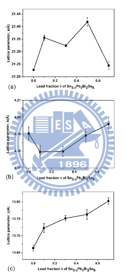
Figure 2.2 Lattice parameters for Sn3-δPbδBi2Se6 (0 ≤ δ ≤ 0.7) as a function
of the Pb composition
18 Figure 2.3 The crystal structure of Sn3-δPbδBi2Se6 as a projection along the
crystallographic b-axis [010]. The slabs exhibit NaCl (311) tilt planes and the atoms along the cell-twinning plane exhibit glide arrayal. Δx indicates the shift in position of the M5 atom from the cell-twinning plane.
28
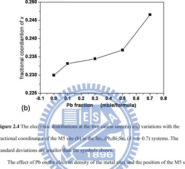
Figure 2.4 The electronic distributions at the five cation sites (a) and variations with the fractional coordinate x of the M5 site (b) in the
Sn3-δPbδBi2Se6 (δ = 0–0.7) systems. The standard deviations are smaller than
the symbols shown.
29
xv
coordinate x of the M5 sites. The black line is the difference in total energy; the energy at x = 0.25 was set to zero for this curve. The blue line shows the ICOHP for the M5 atom vs. fractional coordinate x. The gray area
corresponds to single-crystal results for the Sn3-δPbδBi2Se6 (δ = 0–0.7)
system.
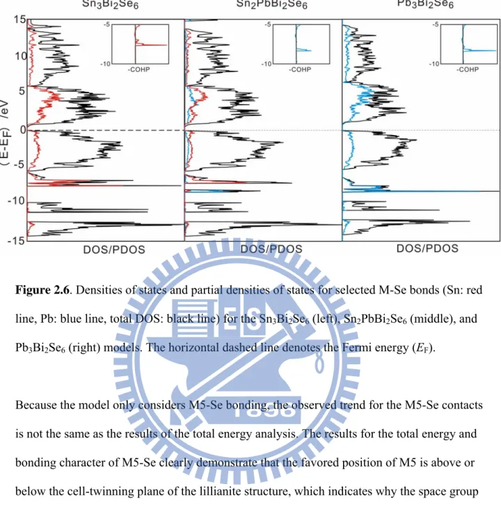
Figure 2.6 Densities of states and partial densities of states for selected M-Se bonds (Sn: red line, Pb: blue line, total DOS: black line) for the Sn3Bi2Se6
(left), Sn2PbBi2Se6 (middle), and Pb3Bi2Se6 (right) models. The horizontal
dashed line denotes the Fermi energy (EF).
32
Figure 2.7 Crystal-orbital Hamiltonian populations (COHP) for selected M-Se interaction curves (M1-Se and M2-Se: black line, M3-Se and M4-Se: red line, and M5-Se: blue line) for Sn3Bi2Se6 (left), Sn2Pb1Bi2Se6 (middle),
and Pb3Bi2Se6 (right).
33
Figure 2.8 Temperature dependence of electrical conductivity (a) and thermoelectric power (b) of Sn3-δPbδBi2Se6 for δ = 0 (light blue), δ = 0.1
(black), δ = 0.3 (red), δ = 0.5 (green) and δ = 0.7 (dark blue).
35
Figure 2.9 Thermal analysis (TG/DTA scans) of Sn3-δPbδBi2Se6 (δ = 0, 0.1,
0.3, 0.5, 0.7)
36
Chapter 3
Figure 3.1 (a)Experimental and simulated X-ray powder patterns for
Pb6-xSnxBi2Se9 (x=0 – 6). (b) The unit cell volume and lattice parameters as a
function of Lead composition in PbxSn6-xBi2Se9 (x= 0 –5).
47
Figure 3.2 The electronic distributions at the five cation sites in the PbxSn6-xBi2Se9 (x = 0–4.36) systems. The standard deviations are smaller
than the symbols shown.
47
Figure 3.3 Crystal structures of PbxSn6-xBi2Se9 (a) projection along [100]
direction with slightly perspective and (b) representation using octahedra chains with the same slab thickness.
49
Figure 3.4 DOS/PDS for series of models: Pb6-xSnxBi2Se9 (x = 0, 3, 6). The
black, red, and blue lines refer to total, Sn and Pb atoms, respectively. The horizontal dashed line denotes the Fermi energy (EF).
51
thermoelectric power (b) of PbxSn6-xBi2Se9 (x=0, 2 and 4).
Figure 3.6 Thermal analysis (TG/DTA scans) of Pb6-xSnxBi2Se9 (x=0, 2 and
4)
54
Chapter 4
Figure 4.1 Experimental and simulated X-ray powder patterns for a) Sn2Pb5Bi4Se13 and b) Sn8.65Pb0.35Bi4Se15.
59 Figure 4.2 Crystal structures of Sn2Pb5Bi4Se13 (a) and Sn8.65Pb0.35Bi4Se15 (b)
in a projection along the crystallographic b-axis [010], showing slabs I, II and III of NaCl (113) tilt planes.
66
Figure 4.3 Density of states (left), partial density of states, and
crystal-orbital hamiltonian populations (COHP) for selected M-Se (M1-Se : black line, M2-Se : red dashed line, and M6-Se : blue line) interactions (right) curves of Sn2Pb5Bi4Se13. The horizontal dashed line denotes the Fermi
energy (EF). The contributions from slab I (M3 (Bi) + M4 (Pb)) and slab II
(M1(Bi) + M2(Bi) + M5(Pb)) are denoted with red and blue lines.
69
Figure 4.4 DOS/PDOS for series of models: SnxPb9-xBi4Se15 (x = 0, 2, 4, 9).
The black, red, and green lines refer to total, Sn and Pb atoms, respectively.
71 Figure 4.5 Density of states (left), partial density of states, and
crystal-orbital hamiltonian populations (COHP) for selected M-Se (M1-Se : black line, M3-Se : blue line, M5-Se : red line and M7-Se : green line) interactions (right) curves of Sn7Pb2Bi4Se15. The horizontal dashed line
denotes the Fermi energy (EF).
72
Figure 4.6 PDOS and COHP plots for Sn9Bi4Se15 (red) and Sn7 Pb2Bi4Se15
(blue). a) PDOS for M7 (M = Sn, Pb). b) COHP for M7-Se contact. The horizontal dashed line denotes the Fermi energy (EF).
72
Figure 4.7 Temperature dependence of electrical conductivity (a) and thermoelectric power (b) of Sn2Pb5Bi4Se13 (black) and Sn8.65Pb0.35Bi4Se15
(red).
74
Figure 4.8 Thermal analysis (TG/DSC scans) of Sn2Pb5Bi4Se13 (a) and
Sn8.65Pb0.35Bi4Se15 (b)
xvii Chapter 5
Figure 5.1 Experimental and simulated X-ray powder patterns for Pb13Sb2.08Bi1.92Se19
79 Figure 5.2 Crystal structures of Pb13Sb2.08Bi1.92Se19 (a) projection along
[010] direction with slightly perspective and (b) representation using octahedra chains with different slab thickness.
86
Figure 5.3 Density of states (left), partial density of states, and
crystal-orbital hamiltonian populations (COHP) for selected M-Se (M2-Se : blue line, M3-Se : black dashed line, and M6-Se : red line) interactions (right) curves of Pb13Sb2.08Bi1.92Se19. The horizontal dashed line denotes the
Fermi energy (EF). The contributions from slab I (M1 (Pb) + M2 (Pb) + M3
(Bi) + M4 (Pb)) and slab II (M5 (Pb) + M6 (Sb) + M7 (Pb) + M8 (Pb)) are denoted with blue and red lines.
88
Figure 5.4 Electrical conductivity and thermal power of Pb13Sb2.08Bi1.92Se19 89 Figure 5.5 Thermal analysis (TG/DTA scans) of Pb13Sb2.08Bi1.92Se19 90
Chapter 6
Figure 6.1 show the structure of Sn4Bi10Se19 andSn8.5Pb1.5Bi18Se37 in a
projection along the crystallographic b-axis [010].
98
Chapter 1
Introduction
1.1. Thermoelectric materials
Energy plays a crucial role in modern society. We all depend on a constant and reliable supply of energy⎯for our homes, businesses, and for transport. It is therefore not surprising
that global warming and fast-rising energy costs have seriously affected our daily life. In
particular, the increase in carbon dioxide emissions from the burning of fossil fuels is believed to be the origin of irreversible climate change. Approximately 90% of the world’s electric power is generated by engines that use fossil fuels and typically operated at ~35% efficiency, with roughly ~65% of heat lost to the environment. Therefore, the reduction in carbon dioxide emissions, either by more efficient use of fossil fuels or greater use of renewable energy, is very important. In this regard, thermoelectric devices are expected to play a vital role in meeting our future energy needs, by enabling a significant reduction in greenhouse gas emissions and our dependence on fossil fuels.
The physics and materials science of thermoelectrics largely developed during two periods of great discovery. In the three decades between 1821 and 1851, the basic
thermoelectric effects were explored and understood macroscopically, and more importantly their applicability to thermometry, power generation, and refrigeration was recognized. With the exception of Altenkirch’s derivation of thermoelectric efficiency in 1911, progress in the field was negligible in the 80 years that followed. Only after the 1930s, the microscopic understanding of electronic interactions in conductors led to the development of
thermoelectric materials currently employed for solid state refrigeration and power generation.1
2
The thermoelectric devices have several obvious advantages when compared with conventional refrigeration systems: (1) Thermoelectric devices can function in environments that are too severe, too sensitive, or too small for conventional refrigeration. (2)
Thermoelectric devices have no moving parts, and no fluids or other materials that require periodic replenishment; theoretically, they can run indefinitely without the need of any kind of maintenance. (3) Highly precise temperature control within ±0.1 oC can be ensured using
thermoelectric devices and appropriate support circuitry. (4) Thermoelectric devices contain no chlorofluorocarbons or other materials which may pollute the environment. (5)
Accelerated life-testing indicated the capability of thermoelectric devices to exceed more than 100 000 hours of steady-state operation. (6) The direction of heat transfer in a thermoelectric system is fully reversible. Changing the polarity of the DC power supply causes heat to be transferred in the opposite direction––a cooler can then become a heater.
According to all the above mentioned advantages, thermoelectric devices have in the last decade found very broad applications in many areas, such as military, aerospace,
instrumentation and sensors, industrial and commercial products2.
Thermoelectric devices are solid-state devices that can convert electrical energy into a temperature gradient or convert thermal energy from a temperature gradient into electrical energy. Traditionally, the term thermoelectricity includes three separately identified
effects⎯the Seebeck effect, the Peltier effect, and the Thomson effect.3-5 The practical
applications of these thermoelectric phenomena remained limited until the development of semiconductor materials.
Among the most important applications of thermoelectric phenomena is thermoelectric refrigeration, which is achieved when a direct current is passed through one or more pairs of n- and p-type semiconductor materials.6 Figure 1.1 is a diagram of a single pair consisting of
to the p-type semiconductor material. The temperature TC of the interconnecting conductor
decreases and heat is absorbed from the environment. This heat absorption from the
environment (cooling effect) occurs when electrons pass from a low energy level in the p-type material through the interconnecting conductor to a higher energy level in the n-type material. The absorbed heat is transferred through the semiconductor materials by electron transport to the other end of the junction of TH temperature and liberated as the electrons return to a lower
energy level in the p-type material. This phenomenon is known as the Peltier effect bears the name of Jean-Charles Peltier, the French physicist who discovered it in 1834.
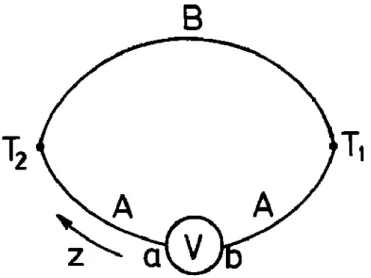
A second phenomenon is also important in thermoelectric refrigeration. When a temperature difference is established between the hot and cold ends of the semiconductor material, a voltage is generated. This voltage is called the Seebeck voltage, and it is directly proportional to the temperature difference. The constant of proportionality, shown in Fig. 1.2, is referred to as the Seebeck coefficient. It is defined as the open circuit voltage produced between two points on a conductor, when a uniform temperature difference of 1 K exists between those points.
Figure 1.1 Schematic of thermoelectric module operation (left) cooling mode; (right) heating mode
4
Figure 1.2 Thermoelectric circuit made of conductors A and B with junction temperatures T1
and T2. Z is the coordinate along the conductors joining the two exits a and b of the voltmeter.
Lastly, William Thomson (Lord Kelvin) predicted and subsequently experimentally observed a third thermoelectric phenomenon, the reversible cooling and heating of a homogeneous conductor when an electrical current flows along it in the presence of a temperature gradient. This is widely known as the Thomson effect and is defined by the rate of heat generated or absorbed in a single current carrying conductor subjected to a
temperature gradient. The Thomson coefficient is unique among the three main thermoelectric coefficients because it is the only thermoelectric coefficient directly measurable for individual materials. The Peltier and Seebeck coefficients can only be determined for pairs of materials.
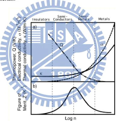
Good thermoelectric materials should possess large Seebeck coefficients and high electrical conductivity, but low thermal conductivity.7, 8 More specifically, a high electrical conductivity is necessary to minimize Joule heating effects, whilst a low thermal conductivity not only helps to retain heat at the junctions, but also to maintain a large temperature gradient. These three properties were later embodied in the so-called figure-of-merit,
where S is the Seebeck coefficient, σ the electrical conductivity and κ the thermal
conductivity. This non-dimensional power generating performance index is used to assess the power generating efficiency of semiconducting materials. The combination of these three properties allows to select the most suitable semiconducting materials for thermoelectric applications on the basis of their capability to attain a maximum value of the product ZT, where T is the absolute temperature (see Fig. 1.3).9 The power obtained depends on efficiency, which is, in turn, determined by the heat flux from the high temperature heat source and the temperature differential during thermoelectric power generation, and the thermoelectric properties of the materials.
Figure 1.3 The Seebeck coefficients, electrical conductivity and thermal conductivity trend of metals, semiconductors, and insulators9.
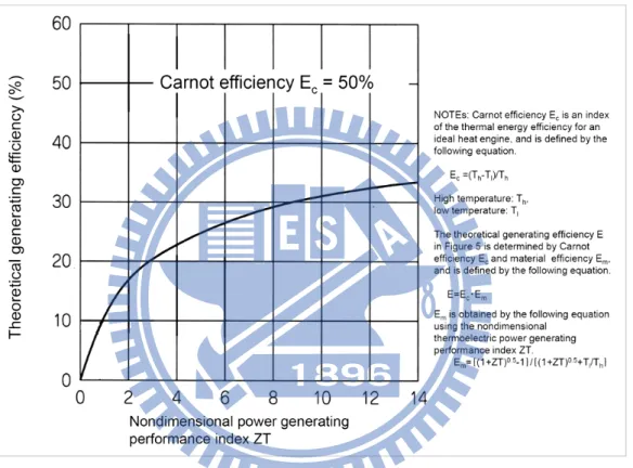
The maximum efficiency of thermoelectric generating systems is given by the Carnot efficiency; this is an index for an ideal heat engine, and the physical properties of the materials, which is termed material efficiency. The relationship between the performance index of a thermoelectric power generating module and the theoretical generating efficiency
6
in the case where the Carnot efficiency is 50% is shown in Fig. 1.4.10 According to this figure, the theoretical generating efficiency approaches the Carnot efficiency as the non-dimensional power generating performance index, ZT, becomes larger. In the current thermoelectric conversion materials in which ZT is approximately equal to 1, theoretical generating efficiency is approximately 9%.
Figure 1.4 Relationship between power generating performance index of thermoelectric power generating module and theoretical generating efficiency10.
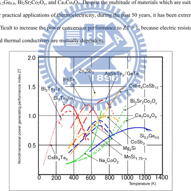
The thermoelectric conversion materials should have a non-dimensional power
generating performance index, ZT, of 2 or higher. The dependence of this power generating performance index of thermoelectric energy conversion materials on temperature is illustrated in Fig. 1.5. To date, the most widely used thermoelectric materials have been intermetallic compounds such as bismuth telluride (Bi2Te3), zinc antimonide (ZnSb) and SiGe. In particular,
Bi2Te3-based compounds have an unusually high ZT value at room temperature, and are
tends to initially increase with increasing temperature and to decrease once a certain temperature has been exceeded. The power generating performance index of Bi2Te3 and
Zn4Sb3 ranges between 1.0 and 1.25 in the low medium temperature region of 300-700 K,
while a compound of AgSbTe2/GeTe (composition ratio 1:1) shows ZT approximately equal
to 1.2 at 700K and Si0.2Ge0.8 shows ZT ≒ 0.7 at approximately 1100K. In the temperature
region under 500 K, BiTe-based compounds display high ZT values. In the medium temperature region of 700-900 K, AgSbTe2/GeTe and CeFe4CoSb12 are high efficiency
materials, and in the high temperature region up to 900 K, the high efficiency materials are Si0.2Ge0.8, Bi2Sr2Co2Oy, and Ca3Co4O9. Despite the multitude of materials which are suitable
for practical applications of thermoelectricity, during the past 50 years, it has been extremely difficult to increase the power conversion performance to ZT > 1, because electric resistance and thermal conductivity are mutually dependent.
Figure 1.5 Temperature dependencies on non-dimensional power generating performance index of main thermoelectric conversion materials11
8
During the 1990s, two approaches developed independently and mostly in different directions. Firstly, nanoscale constituents, prepared by different chemical approaches were introduced to the most prominent of bulk thermoelectric materials. 12-15 Secondly,
low-dimensional materials systems were now being assembled as three-dimensional nanocomposites containing a coupled assembly of nanoclusters showing short-range low dimensionality embedded in a host material,1, 16 thereby producing a bulk material with nanostructures and many interfaces that scatter phonons more effectively than electrons.
Among chalcogenides, Bi2-xSbxTe3-ySey is the best known thermoelectric material that
has long served the needs of cooling applications at ambient temperature (ZT ~ 1).9 Recently, two new materials were identified, CsBi4Te6 and AgPbmSbTe2+m which show good
thermoelectric properties (ZT = 0.82 and 2.2) at both low and high temperature.17, 18 In addition, new techniques have been developed for the deposition of nanometer-sized
thermoelectric materials on thin films. Some rational approaches to the development of future solid-state systems include materials with a large ZT value, such as clatherate19-21 and
skutterudite22, 23 phases. Lastly, chalcogenides that contain heavy main-group elements and
exist in minerals and synthetic compounds have attracted intensive research for their prospective applications in thermoelectric devices.
1.2. Homologous series
A series of structures built on the same structural principle with certain building blocks expanding by regular increments is called a homologous series. This could be built through the addition of a layer or a row of atoms on a given block. A homologous series is expressed by means of a mathematical formula that has ability to reproduce each member. It is a useful tool for designing compounds, because it allows a modular classification of its members, while concentrating on large scale structural features. The classification of the building blocks (or called modules) requires a certain level of abstraction with respect to the atomic
occupancy and bonding details. The efficacy of a given homology depends on its ability to generate an infinite number of structure types.
Complex structures can be assembled from one, or more kinds of building blocks. Generally, the building blocks of a homologous series of compounds are simple, common units that adopt archetypal structures or are excised from such structures (e.g., NaCl-type blocks). To form each member, these building blocks need to combine in various ways according to the principles of coordination chemistry or by the action of structure building operators, unit cell intergrowth, glide reflection twinning, cyclic twinning, etc.24 Within a homologous series, the type of fundamental building units and the principles that define how they combine remain preserved. Only the size of the building blocks can varies incrementally by changing the number of coordination polyhedra.
The term homologous series was used to describe chemical series that can be expressed by a general mathematical formula and built on the same structural principles,25 first in complex metal oxide systems26, 27 and later in intermetallics, chalcogenides, 28, 29 etc. Several homologous series are known for sulfides; these include the kobellite series,30 the pavonite series,31 the gustavite-lillianite series.32 In addition, it was found that the BaQ/Fe2Q3 system
10
et al. studied a new homologous series of Am[M1+lSe2+l]2m[M2l+nSe2+3l+n], where A denotes an
alkali or alkaline earth element; M is a main-group metal; and the three integer variables, l, m, and n, are used to control the shape or size in this series.34, 35
The lillianite homologous series has also been investigated by Kanatzidis et al.36 On the other hand, the first sample of lillianite (Pb3Bi2S6), a rare Pb-Bi sulfosalt, were found37and
defined38, 39 by Makovicky et al. Its members are generated by tropochemical cell twinning on to the (311) plane of slabs of galena (NaCl-type) lattices with a mirror as twin operation and reflecting the lattices across the mirror planes at z=±1/4. In different lillianite homologous series in the thickness of the NaCl-type building blocks varies. Tropochemical cell twinning is a twinning on the cell scale which has been reported for minerals. This phenomenon takes place during those structural changes that are accompanied by a change in chemical composition. It can also be considered as a stress-relieving mechanism that accommodates impurities in the crystal. Figure 1.6 depicts the Pb3Bi2S6 structure with tropochemical cell
twinning. The various members of the lillianite homologous series can be identified by the number of metal octahedral along the (111) direction of the galena slabs.
The structures of the lillianite homologous series are described by the symbols L, n, n', where L indicates a member of the lillianite series, and n and n' correspond to the number of octahedra between two sides of the tropochemical cell-twinning plane. The symbol L(n, n') reflects the cation/anion ratio (M/X). The limit of the M/X ratio is located between 1 (PbS for L(∞,∞) ) and 0.714 (PbBi4S7 for L(2,1)). In the polysynthetic twinning in NaCl-(311) type,
the M/X ratio decreases with increasing number of octahedral, n. For example, the mineral lillianite, Pb3Bi2S6, is denominated as L (4, 4) and KxSn6-2xBi2+xSe9 as L (7, 7), where the
symbols mean that two identical, 4 and 7, octahedral blocks undergo cell-twinning. The sulfosalts of the lillianite family with a known structure are summarized in Table 1.1. In lillianite, three Pb2+ ions in galena have been placed by two Bi3+ ions, and one cation site has been eliminated,
6PbS→3PbS+Bi2S3.
There is a 16.67% (1/6) “cation deficiency” as compared with perfect galena (PbS).
Table 1.1 The sulfosalts with known structures of lillianite family40, 41
Ideal composition symbol L(N,N') Species X/M M/X Galena, PbS 1.000 1.000 (∞,∞) Ourayaite, Ag12.5Pb15Bi20.5S52 1.083 0.923 (11,11) Heyrovskite, Pb5.4Bi2.42Ag0.18S9 1.125 0.889 (7,7) Eskimoite, Ag7Pb10Bi15S36 1.125 0.889 (9,5) Treasurite, Ag7Pb6Bi15S32 1.143 0.875 (8,4) Vikingite, Ag5Pb8Bi13S30 1.154 0.867 (7,4) Lillianite, Pb3Bi2S6 1.200 0.833 (4,4) Benjaminite, Ag3Bi7S12 1.200 0.833 (4,4) Gustavite, AgPbBi3S6 1.200 0.833 (7,1) Pavonite, AgBi3S5 1.250 0.800 (5,1) Cu3.21Bi4.79S9 1.286 0.778 (4,1) CuBi5S8 1.333 0.750 (3,1) Pb2Bi6S11 1.375 0.727 (2,2,1) Pb3Bi10S18 1.385 0.722 (2,2,1,2,1) PbBi4S7 1.400 0.714 (2,1)
12 1.3. Motivation and goal of this thesis
Post-transition-metal ions such as Bi3+ and Pb2+ often generate distorted coordination environments associated with the inert lone electron pair42-44. The chalcogenide compounds formed by combinations of such ions usually exhibit complex crystal structures and
semiconducting properties with a narrow band gap, and are promising materials for nonlinear optics45, ferroelectrics46, and thermoelectrics47-49. In a synthesis of new materials with useful thermoelectric properties, heavy main-group elements, such as tin, lead, antimony and bismuth, might enhance the electrical conductivity and diminish the thermal conductivity. Materials in this class contain various coordination environments constructed from M2+ (M = Sn, Pb) and M3+ (M = In, Sb, Bi) centers and Se2- ions assembled into a structure similar to
lillianite. These structures are homologous, with ordered intergrowths of “galena-like” structures cut parallel to the (311) plane to form a number of diverse frameworks with
chemically twinned arrangements, a current theme in crystal chemistry that has recently been reviewed38, 50-52. Many naturally occurring minerals and synthetic lillianite-type chalcogenides have been studied, including PbBi4S7 [L (2,1)]53; CuBi5S8 [L (3,1)]54; Cu3.21Bi4.79S9 [L (4,1)]55;
AgBi3S5 [L (5,1)]56; Pb3Bi2S637, 57, AgPbBi3S658,and AgPbSb3S6 [L (4,4)]59; Ag5Pb8Bi13S30 [L
(4,7)]39; Pb6Bi2S960and K0.54Sn4.92Bi2.54Se9 [L(7,7)]36; Ag3Bi7S12 [L (7,1)]61; KSn5Bi5Se13
[L(4,5)]36; Ag7Pb6Bi15S32 [L (4,8)]62; Ag7Pb10Bi15S36 [L (5,9)]38; and Ag12.5Pb15Bi20.5S52 [L
(11,11)]50. Most of the above lillianite-type chalcogenides are sulfosalts; only a few selenides have been reported. Recently, we have demonstrated that multinary selenides, such as
InSn2Bi3Se863, InSn6BiSe9 and Pb4InxM6-xSe13 (M = Bi, x = 2.1–2.8; Sb, x = 2)64, can be
prepared through solid-state synthetic routes that comprise various building units. Theoretical calculations have shown that the mixed occupancy metal sites arise from optimized M-Se bonding.
main-group elements. On introducing heavy main-group elements such as Pb and Bi, an intriguing feature is the stereochemical localization of their ns2 electrons that might influence the structural type and electronic structure, and consequently the electronic properties of the resulting compounds. Here we report the synthesis, structural characterization, measurements of physical properties, and calculations of electronic structures of five new quaternary
selenides Sn3-δPbδBi2Se6 (δ = 0 – 0.7), PbxSn6-xBi2Se9 (x = 0 – 4.36), Sn2Pb5Bi4Se13,
Sn8.65Pb0.35Bi4Se15 and Pb13Sb2.08Bi1.92Se19. First two compounds contained a measurable
phase width and the other compounds have no phase width. The compounds of Sn3-δPbδBi2Se6
(δ = 0.0 – 0.7) were synthesized and their structures are related to that of Pb3Bi2S6 with an
atomic position near the cell-twinning plane. Band structure calculations indicated that the structure is stabilized when the position of the M5 site is farther from the cell-twinning plane. The substitution of lead for tin cations in PbxSn6-xBi2Se9 because of the similar bonding
strength in Pb/Sn atoms and varying the Pb/Sn ratio produces significant variation of the physical and electronic properties. Quaternary selenides Sn2Pb5Bi4Se13 and Sn8.65Pb0.35Bi4Se15
exhibit tropochemical cell-twinning of NaCl-type structures with lillianite homologous series L(4, 5) and L(4, 7), respectively. Pb13Sb2.08Bi1.92Se19 reveals novel structure type with
alternated 7 and 8 octahedra wide slabs. Calculations of band structures, measurements of Seebeck coefficient and electrical conductivity confirm that these compounds are
14 Chapter 2
Experimental and Theoretical Studies of Sn3-δPbδBi2Se6 (δ = 0.0–0.7)
Abstract
New ternary and quaternary chalcogenides Sn3-δPbδBi2Se6 (δ = 0.0–0.7), were
synthesized from pure elements using the solid-state method. Their crystal structures, determined using single crystal X-ray diffraction, belong to the orthorhombic space group
Pnma (No. 62). The structure is related to Pb3Bi2S6 that contains NaCl [311] layer units and
zigzag arrays of metal atoms along the c-axis. A correlation between the Pb composition and the shifted position of a metal site was observed. Band structure calculations confirmed that the structure is stabilized when the position of the M5 site is farther from the mirror plane. Thermopower and conductivity measurements indicated that all of the compounds are n-type semiconductors with small band gaps.
2.1 Experiments 2.1.1 Synthesis
All reactions were carried out in a glovebox under a dry nitrogen atmosphere. The
elements were used as received: Sn powder, Alfa 99.5%; Bi powder, Alfa 99.95%; Pb powder, Alfa 99%; and Se powder, Alfa 99.9%. In a typical reaction, all compounds were obtained by heating a stoichiometric mixture of the elements in evacuated quartz tubes to 1073 K over 12 hr, holding at 1073 K for 18 hr, slow cooling to 773 K at a rate of 0.42 K min-1, and then cooling to room temperature naturally. Compound (1), Sn3Bi2Se6, was initially obtained from
a reaction intended to synthesize “Sn5Bi6Se14” through the solid-state method. Based on
powder X-ray diffraction results, the product of the “Sn5Bi6Se14” reaction yielded an unknown
phase after a search of the JCPDF database. A cuboid-shaped crystal was selected for
single-crystal X-ray diffraction measurements. The refined formula Sn3Bi2Se6 was determined,
which was then used to synthesize the pure phase under the same heating conditions specified above. Attempts to obtain the charge-balanced product Sn3Bi2Se6 failed; the reaction product
contained a mixture of Sn3Bi2Se6 and SnSe2 phases. Reactions of Sn3-γBi2+γSe6 (0 ≤ γ ≤ 1) with
Sn2.67Bi2.26Se6 (refined formula with vacancies) were conducted to probe the possible phase.
Two temperature profiles with slow cooling as described above and a quench reaction at 1073 K were performed. For reactions using the slow cooling process, a pure phase was obtained with γ = 0.38 and Sn2.67Bi2.26Se6 (refined formula). Products of the other reactions contained
the primary phase and impurities of SnSe2 and Sn3Bi2Se6. For reactions using the quenching
process, products of reactions with 0 ≤ γ ≤ 0.62 yielded similar powder X-ray patterns to Sn2.67Bi2.26Se6 with a broad peak width, indicative of poor crystallinity, with which it was
impossible to perform a single-crystal study. For the quaternary system, a series of reactions with Sn3-δPbδBi2Se6 (0 ≤ δ ≤ 2) were performed to investigate the phase width under the same
16
obtained when 0.1 < δ < 0.7 (Figure 2.1a). The calculated lattice parameters a and b exhibited weak correlations with the percent Pb composition, while the lattice parameter c expanded as the concentration of Pb increased in the framework (Figure 2.2). The effect of percent Pb composition on the cell volume is shown in Figure 2.1b, indicating that the cell volume varies from 1204(2) Å3 for Sn3Bi2Se6 (x = 0) to 1230(2) for Sn2.3Pb0.7Bi2Se6 (x = 0.7). The PbSe
impurity phase began to form when δ > 0.7. Crystals from the δ = 0.1, 0.3, 0.5, and 0.7 reactions were selected for single-crystal X-ray analysis.
2.1.2 Single-crystal X-ray Diffraction (XRD)
Cuboid-shaped crystals obtained for Sn3-δPbδBi2Se6 [δ = 0.0 (1), 0.1 (2), 0.3 (3), 0.5 (4),
and x = 0.7 (5)] were mounted on a glass fiber with epoxy glue for single-crystal X-ray diffraction analysis. Intensity data were collected using a diffractometer (Bruker APEX CCD equipped with graphite-monochromated Mo-Kα radiation, λ = 0.71073 Å) at 300 K. The crystal-to-detector distance was 5.038 cm and the exposure time was 30 s. Data were collected with a scan width of 0.3° in ω with four groups of 600 frames at ψ settings of 0°, 90°, 180°, and 270°. The 2θ values ranged between 1.76° and 56.54°. Diffraction peaks obtained from all frames of the reciprocal space images were integrated and used to determine the unit cell parameters using the Siemens SAINT program. The data were corrected for Lorentz and polarization effectsusing SADABS65. Absorption corrections were based on a function fitted to the empirical transmission surface sampled by multiple equivalent
measurements of numerous reflections. The structural model was obtained using the direct method and refined by full-matrix least-squares refinement based on F2 using the SHELXTL package66.
Figure 2.1 (a) Experimental and simulated powder X-ray patterns Sn3-δPbδBi2Se6 (δ = 0 –0.7).
18
Figure 2.2 Lattice parameters for Sn3-δPbδBi2Se6 (0 ≤ δ ≤ 0.7) as a function of the Pb
All compounds had an orthorhombic lattice. Analysis of the systematic absence of reflections for compounds 1, 2, and 3 suggested space group Pnma (No. 62). In the structural refinement process, a structural model was determined having five unique sites containing metal atoms (Sn, Bi, and Pb) and six unique sites containing Se atoms. The occupancy
parameters were refined along with the displacement parameters. The results indicated that all Se sites were fully occupied and the M1-M5 sites had mixed occupancies. The calculated electron densities of the M1-M5 sites were within 50–81 electrons/site, which were refined to fully occupied Sn (M3 site in compound 1) or mixed occupancy Sn/Bi or Sn/Pb sites. The final cycle of refinement included anisotropic displacement parameters and a secondary extinction correction performed on F2. For compound 1, the refinement of metal sites suffers
from strong correlation between site occupancy and displacement parameter due to the poor X-ray diffraction data. The refinements indicate different electron densities in M1-M5 sites, and subsequently the site composition were estimated from the refined electron densities and fixed in the final stage of refinement. Fourier maps from 1, 2 and 3 reveal residual peaks ~3.8–4.3 e-/Å3 close to M5 (~0.9 Å). The refined compositions for 1, 2, and 3 were
(Sn+2)3(Bi+3)2(Se-2)6, (Sn+2)2.93(Pb+2)0.19(Bi+3)1.89(Se-2)6, and (Sn+2)2.67(Pb+2)0.32(Bi+3)2(Se-2)6,
respectively, consistent with reaction stoichiometry.
Compounds 4 and 5 were initially refined with the C-centered space group Cmcm (No. 63), and structural refinements yielded reasonable values for R1/wR2 (4: 4.76%/11.85%, 5: 3.07%/7.08%). However, the anisotropic displacement factors for the position on the mirror plane (M5 site) had unreasonable values (~0.181 and ~0.126 Å2 along the a-axis for 4 and 5, respectively). These values could reflect partially occupied Sn or Bi sites, but the refined formulae were not charge-balanced and did not justify this refinement. Ultimately, the Pnma space group was chosen and the assignments for the metal and Se sites were similar to those
20
of 1–3. The final refinements yielded charge-balanced formulae for 4 and 5 of
(Sn+2)2.49(Pb+2)0.42(Bi+3)2.09(Se-2)6 and (Sn+2)2.1 (Pb+2)0.67(Bi+3)2.23(Se-2)6, respectively.
Crystallographic data and selected bond distances for compounds 1–5 are given in Tables 2.1, 2.2 and 2.3.
Table 2.1 Crystallographic Data for Sn3-δPbδBi2Se6. (δ = 0, 0.1, 0.3, 0.5, 0.7) Empirical formula Sn3Bi2Se6(1) Sn2.9Pb0.1Bi2Se6 (2) Sn2.7Pb0.3Bi2Se6(3) Sn2.5Pb0.5Bi2Se6(4) Sn2.3Pb0.7Bi2Se6 (5) Refined formula Sn3Bi2Se6 Sn2.93(6)Pb0.19(3)Bi1.89(5)Se6 Sn2.67(6)Pb0.32(4)Bi2.00(6)Se6 Sn2.49(4)Pb0.42(2)Bi2.09(4)Se6 Sn2.1(3)Pb0.67(1)Bi2.23(3)Se6 Formula weight 1247.79 1256.64 1274.34 1292.04 1309.74 Temperature, K 300(2) 300(2) 300(2) 300(2) 300(2) Wavelength, Å 0.71073 0.71073 0.71073 0.71073 0.71073 Crystal system Orthorhombic Orthorhombic Orthorhombic Orthorhombic Orthorhombic Space group Pnma (No. 62) Pnma (No. 62) Pnma (No. 62) Pnma (No. 62) Pnma (No. 62)
Unit cell dimensions, a a = 21.213(6) Å a = 21.373(4) Å a = 21.365(6) Å a = 21.399(8) Å a = 21.235(8) Å b b = 4.162(1) Å b = 4.1898(8) Å b = 4.190(1) Å b = 4.190(2) Å b = 4.198(2) Å c c = 13.640(4) Å c = 13.690(2) Å c = 13.741(4) Å c = 13.797(5) Å c = 13.846(6) Å Volume, Å3 1204.2(6) 1226.0(4) 1230.2(6) 1239.7(8) 1234.3(9) 4 4 4 4 4 Density (calculated), Mg/m3 6.883 6.808 6.881 6.923 7.048 Absorption coefficient, mm-1 53.343 53.56 55.71 57.589 60.161 F(000) 2080 2092.8 2118.4 2144 2170 Crystal size, mm3 0.1 × 0.03 × 0.03 0.08 × 0.03 × 0.03 0.1 × 0.05 × 0.04 0.08 × 0.03 × 0.03 0.08 × 0.04 × 0.03 Reflections collected 10884 8871 8866 8732 14065 Independent reflections 1701 [R(int) = 0.0455] 1721 [R(int) = 0.0388] 1734 [R(int) = 0.0333] 1744 [R(int) = 0.0571] 1746 [R(int) = 0.0492]
Completeness to theta = 28.24 99.90% 99.90% 99.50% 99.90% 99.80% Data / restraints / parameters 1701 / 0 / 67 1721 / 0 / 73 1734 / 0 / 73 1744 / 0 / 72 1746 / 0 / 72 Goodness-of-fit on F2 1.913 1.078 1.082 1.059 1.114
Final R indices [I > 2σsigma(I)] R1 = 0.0556, wR2 = 0.1310 R1 = 0.0319, wR2 = 0.0774 R1 = 0.0349, wR2 = 0.0792 R1 = 0.0467, wR2 = 0.1193 R1 = 0.0493, wR2 = 0.0975 Largest diff. peak and hole 4.765 and -3.348 e/Å3 3.836 and -2.35 e/Å3 3.91 and -2.873 e/Å3 5.846 and -4.778 e/Å3 2.942 and -3.985 e/Å3
22
Table 2.2 Selected Interatomic Distances in Å for Sn3-δPbδBi2Se6(δ=0 – 0.7)
δ 0 0.1 0.3 0.5 0.7 M1—Se6 2.785(2) 2.792(2) 2.794(2) 2.798(2) 2.780(1) M1—Se8 × 2 2.866(1) 2.877(3) 2.884(1) 2.889(1) 2.888(2) M1—Se9 × 2 3.033(1) 3.024(1) 3.036(3) 3.043(2) 3.047(1) M1—Se10 3.081(2) 3.067(1) 3.082(2) 3.086(2) 3.069(1) M2—Se7 × 2 2.841(1) 2.860(2) 2.865(3) 2.875(3) 2.892(1) M2—Se7 3.122(2) 3.179(1) 3.189(1) 3.227(3) 3.307(2) M2—Se8 2.844(2) 2.834(1) 2.831(2) 2.828(1) 2.784(1) M2—Se10 × 2 3.086(1) 3.098(1) 3.083(1) 3.076(2) 3.044(1) M3—Se6 2.798(2) 2.825(1) 2.816(1) 2.815(1) 2.778(2) M3—Se7 × 2 3.039(2) 3.060(2) 3.055(1) 3.054(2) 3.049(2) M3—Se10 2.975(2) 3.024(2) 3.027(1) 3.043(1) 2.053(1) M3—Se11 × 2 2.834(2) 2.848(1) 2.854(2) 2.738(2) 2.879(1) M4—Se9 × 2 2.977(2) 2.984(1) 2.970(2) 2.963(1) 2.919(1) M4—Se10 × 2 2.947(2) 2.982(2) 2.989(2) 3.001(2) 3.019(2) M4—Se11 2.709(2) 2.728(1) 2.728(4) 2.738(2) 2.759(2) M4—Se9 3.490(2) 3.513(2) 3.499(1) 3.487(3) 3.381(2) M5—Se6 × 2 2.861(2) 2.868(2) 2.876(1) 2.884(2) 2.881(2) M5—Se9 2.829(2) 2.893(1) 2.970(2) 3.071(2) 3.377(3) M5—Se11 × 2 3.194(2) 3.239(1) 3.241(1) 3.258(2) 3.303(2) M5—Se8 × 2 3.459(1) 3.451(2) 3.438(1) 3.429(3) 3.344(1) Table 2.3a Fractional Atomic Coordinates and Equivalent Isotropic Atomic Displacement
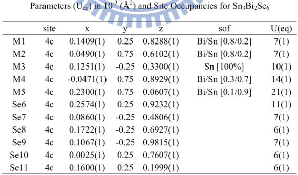
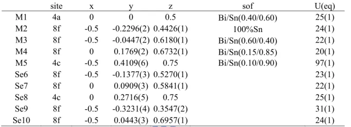
Parameters (Ueq) in 10-3 (Å2) and Site Occupancies for Sn3Bi2Se6
site x y z sof U(eq)
M1 4c 0.1409(1) 0.25 0.8288(1) Bi/Sn [0.8/0.2] 7(1) M2 4c 0.0490(1) 0.75 0.6102(1) Bi/Sn [0.8/0.2] 7(1) M3 4c 0.1251(1) -0.25 0.3300(1) Sn [100%] 10(1) M4 4c -0.0471(1) 0.75 0.8929(1) Bi/Sn [0.3/0.7] 14(1) M5 4c 0.2300(1) 0.75 0.0607(1) Bi/Sn [0.1/0.9] 21(1) Se6 4c 0.2574(1) 0.25 0.9232(1) 11(1) Se7 4c 0.0860(1) -0.25 0.4806(1) 7(1) Se8 4c 0.1722(1) -0.25 0.6927(1) 6(1) Se9 4c 0.1067(1) -0.25 0.9815(1) 7(1) Se10 4c 0.0025(1) 0.25 0.7607(1) 6(1) Se11 4c 0.1600(1) 0.25 0.1999(1) 6(1)
Table 2.3b Fractional Atomic Coordinates and Equivalent Isotropic Atomic Displacement Parameters (Ueq) in 10-3 (Å2) and Site Occupancies for Sn3-δPbδBi2Se6. (δ = 0.1)
site x y z Sof U(eq)
M1 4c 0.3597(1) 0.25 0.1697(1) Bi/Sn [0.812(7)/0.188] 18(1) M2 4c 0.0496(1) -0.75 -0.1119(1) Bi/Sn [0.840(7)/0.160] 17(1) M3 4c 0.1250(1) 0.25 0.1698(1) Sn/Bi [0.936(6)/0.064] 16(1) M4 4c 0.4528(1) -0.75 -0.1045(1) Sn/Bi [0.831(6)/0.169] 21(1) M5 4c 0.2669(1) -0.25 -0.0610(1) Sn/Pb [0.814(7)/0.186] 34(1) Se6 4c 0.2432(1) 0.25 0.0774(1) 20(1) Se7 4c 0.0865(1) -0.25 0.0182(1) 18(1) Se8 4c 0.3288(1) -0.25 0.3054(1) 18(1) Se9 4c 0.3923(1) -0.25 0.0187(1) 18(1) Se10 4c 0.4965(1) 0.25 0.2378(1) 17(1) Se11 4c 0.1593(1) -0.25 0.3002(1) 16(1)
Table 2.3c Fractional Atomic Coordinates and Equivalent Isotropic Atomic Displacement Parameters (Ueq) in 10-3 (Å2) and Site Occupancies for Sn3-δPbδBi2Se6. (δ = 0.3)
site x y z sof U(eq)
M1 4c 0.3606(1) 0.25 0.1685(1) Bi/Sn [0.797(8)/0.203] 20(1) M2 4c 0.0495(1) -0.75 -0.1117(1) Bi/Sn [0.820(8)/0.18] 19(1) M3 4c 0.1261(1) 0.25 0.1680(1) Sn/Bi [0.884(7)/0.116] 17(1) M4 4c 0.4521(1) -0.75 -0.1070(1) Sn/Bi [0.721(7)/0.279] 23(1) M5 4c 0.2655(1) -0.25 -0.0631(1) Sn/Pb [0.677(8)/0.323] 38(1) Se6 4c 0.2440(1) 0.25 0.0763(1) 23(1) Se7 4c 0.0870(1) -0.25 0.0180(1) 22(1) Se8 4c 0.3294(1) -0.25 0.3044(1) 19(1) Se9 4c 0.3946(1) -0.25 0.0175(1) 22(1) Se10 4c 0.4972(1) 0.25 0.2406(1) 18(1) Se11 4c 0.1603(1) -0.25 0.2987(1) 19(1)
24
Table 2.3d Fractional Atomic Coordinates and Equivalent Isotropic Atomic Displacement Parameters (Ueq) in 10-3 (Å2) and Site Occupancies for Sn3-δPbδBi2Se6. (δ = 0.5)
site x y z sof U(eq)
M1 4c 0.2619(1) 0.25 0.1671(1) Bi/Sn [0.718(5)/0.282] 17(1) M2 4c 0.0497(1) -0.75 -0.1118(1) Bi/Sn [0.789(2)/0.211] 15(1) M3 4c 0.1273(1) 0.25 0.1664(1) Sn/Bi [0.804/0.196(3)] 17(1) M4 4c 0.4515(1) -0.75 -0.1087(1) Sn/Bi [0.616(8)/0.384] 18(1) M5 4c 0.2632(1) -0.25 0.0649(1) Sn/Pb [0.584(4)/0.416] 38(1) Se6 4c 0.2451(1) 0.25 0.757(1) 17(1) Se7 4c 0.0883(1) -0.25 0.0175(1) 18(1) Se8 4c 0.3303(1) -0.25 0.3024(1) 14(1) Se9 4c 0.3967(1) -0.25 0.0168(1) 18(1) Se10 4c 0.4977(1) 0.25 0.2427(1) 13(1) Se11 4c 0.1614(1) -0.25 0.2976(1) 14(1)
Table 2.3e. Fractional Atomic Coordinates and Equivalent Isotropic Atomic Displacement Parameters (Ueq) in 10-3 (Å2) and Site Occupancies for Sn3-δPbδBi2Se6. (δ = 0.7)
site x y z sof U(eq)
M1 4c 0.3655(1) 0.25 0.1646(1) Bi/Sn [0.492(1)/0.508] 21(1) M2 4c 0.0498(1) -0.75 -0.1117(1) Bi/Sn [0.674(3)/0.326] 19(1) M3 4c 0.1314(1) 0.25 0.1644(1) Sn/Bi [0.579/0.421(7)] 25(1) M4 4c 0.4505(1) -0.75 -0.1114(2) Sn/Bi [0.354(4)/0.646] 23(1) M5 4c 0.2535(1) -0.25 -0.0676(1) Sn/Pb [0.334(1)/0.666] 63(1) Se6 4c 0.2484(1) 0.25 0.0747(1) 24(1) Se7 4c 0.0929(1) -0.25 0.0160(1) 24(1) Se8 4c 0.3328(1) -0.25 0.2988(1) 18(1) Se9 4c 0.4030(1) -0.25 0.0157(1) 25(1) Se10 4c 0.4994(1) 0.25 0.2481(1) 17(1) Se11 4c 0.1649(1) -0.25 0.2971(1) 18(1)
2.1.3 Characterization
X-ray powder diffraction analysis of the products was performed using a
Bragg–Brentano-type powder diffractometer (Bruker D8 Advance, operated at 40 kV and 40 mA, Cu Kα, λ = 1.5418 Å). For phase identification, XRD data were collected over a 2θ range from 5° to 90° with a step interval of 0.05°. The bond valence calculations were performed using valence bond theory with R0 values of 2.59, 2.67, and 2.72 Å for Sn2+, Pb2+, and Bi3+,
respectively67.
Energy dispersive spectra (SEM/EDX, Hitachi S-4700I High-Resolution Scanning Electron Microscope) were recorded for the cuboid crystalline samples. Semiquantitative EDS analysis of individual crystals of each reaction product confirmed the presence of Sn, Pb, Bi, and Se. Differential thermal analyzer (DTA) and thermogravimetry (TG) measurements were performed using a thermal analyzer (NETZSCH STA 409PC). A powder sample
(approximately 30 mg) was placed in an alumina crucible; Al2O3 powder served as a
reference sample. The sample was heated to 1273 K at 20 K/min under a constant flow of N2.
2.1.4 Physical Property Measurements
Seebeck coefficients were measured on a cold-pressed bar (1×1×5 mm3) with a
commercial thermopower measurement apparatus (MMR Technologies) over the temperature range 300–500 K under a dynamic vacuum (~10-2 Torr). Constantan served as an internal standard and silver conductive paint was used to create electrical contacts. DC conductivity measurements were performed using a standard four-probe method with a homemade device under vacuum (~10-2 Torr) over the temperature range 100–300 K. Electrical contacts
consisted of four copper wires attached to the bulk with silver glue. Samples were placed under a vacuum for air at least 1 hour to allow the silver glue to dry completely, which improved contact performance. To minimize the effects of grain boundaries in the crystalline
26
powder on the conductivity measurements, each cold-pressed sample was annealed at 773 K for 72 h before measurement.
2.1.5 Theoretical Calculations
Self-consistent tight-binding linear muffin tin orbital (LMTO) calculations using the atomic spheres approximation (ASA) were undertaken to investigate the electronic structures of these compounds. The density-function theory was applied with the local density
approximation (LDA)68-72. The atomic radii used were 1.72, 1.63, and 1.22 Å for Sn, Bi, and Se, respectively. All k-space integrations were performed with the tetrahedron method on 16 × 16 × 8 grids of unique k points in the first Brillouin zone. Within the Brillouin zone based on the primitive cell of Sn3Bi2Se6, 288 irreducible k points were used. We analyzed the
electronic structure by extracting information from the densities of states (DOS) and the curves for crystal-orbital Hamiltonian populations (COHP)73. To understand the effects of the M5 position and Pb concentration on the electronic structure, stability, and bonding of the as-synthesized compounds, two models were constructed of the electronic structure: (a) Sn3Bi2Se6 with the cation sites assigned to Bi(M1, M2) and Sn(M3-M5) in space group Pnma,
and with the fractional coordinate x of the M5 site ranging from x = 0.225 to x = 0.25 (on the mirror plane); (b) Sn3-δPbδBi2Se6 (δ = 0, 1, and 3) with varied assignments of metal sites.
Details of the models are described in Table 2.4.
Table 2.4. Three models with varied assignments of metal sites for LMTO calculations. Sn3Bi2Se6 Sn2Pb1Bi2Se6 Pb3Bi2Se6 M1 Bi Bi Bi M2 Bi Bi Bi M3 Sn Sn Pb M4 Sn Sn Pb M5 Sn Pb Pb Se6–Se11 Se Se Se
2.2 Results and Discussion 2.2.1 Crystal Structure
The crystal structures of compounds 1–5 are closely related to that of lillianite Pb3Bi2S6.
These as-synthesized phases contain four formulas per unit cell, with eleven
crystallographically inequivalent sites: four with mixed-occupancy cations Sn2+/Bi3+, one with Sn2+/Pb2+ or fully occupancy Sn2+, and six with Se2-. The structure is illustrated in Figure 2.3 as a projection along the crystallographic b-axis (010). The structure contains two slabs of the same thickness that exhibit NaCl (311) tilt planes expanding along the a, b direction, which are connected by a Se6 atom to form a three-dimensional structure. The same structural feature exists in KSn5Bi5Se1336 and InSn6BiSe963, which contain similar NaCl(311)-type layer
units. The lillianite phase Pb3Bi2S6 also contains a metal site on the cell-twinning plane
showing mirror symmetry. However, the M5 metal sites in the present selenides exhibit a zigzag array along the c-axis with glide symmetry. The coordination environments of the metal sites fall into two groups. (i) The M1-M4 sites are six-coordinate, with two types of distorted octahedral environments. The first type is a square pyramid having one short (~2.73 Å), four intermediate (2.92–3.02 Å), and one longer (~3.5 Å) bond trans to the shorter M-Se distances. The second type is a trigonal pyramid with three short M-Se bonds (2.7–2.9 Å) opposite to three longer ones (2.9–3.1 Å). (ii) The M5 site is close to the pseudo mirror plane with zigzag arrays along the (001) direction, as shown in Figure 2.3. Its coordination
geometry can be described as a monocapped trigonal prism with M5-Se distances varying between 2.861(2) and 3.459(1) Å. The M-Se distances in both structures are comparable to a binary system and some multinary selenides in the literature that contain mixed occupancies of Bi/Sn or Pb/Sn, such as Pb4Sb4Se1074, Pb0.875Sn0.125Se75, PbBi2Se476, InSn2Bi3Se863, and
28 Figure 2.3 The crystal structure of Sn3-δPbδBi2Se6 as a projection along the crystallographic
b-axis [010]. The slabs exhibit NaCl (311) tilt planes and the atoms along the cell-twinning
plane exhibit glide arrayal. Δx indicates the shift in position of the M5 atom from the cell-twinning plane.
Figure 2.4 The electronic distributions at the five cation sites (a) and variations with the fractional coordinate x of the M5 site (b) in the Sn3-δPbδBi2Se6 (δ = 0–0.7) systems. The
standard deviations are smaller than the symbols shown.
The effect of Pb on the electron density of the metal sites and the position of the M5 site was studied and the results are shown in Figure 2.4a. For ternary phase 1 and quaternary phases with a low Pb content, the refined electron count for metal sites fell into two groups with electrons ~78 (M1, M2) and ~55 e-/site (M3, M4, M5), located in different NaCl(311) slab units (Figure 2.3). As the Pb concentration was increased, the electron densities of the M1 and M2 sites decreased, while those of the M3-M5 sites increased (Figure 2.4a). The refined electron count of the metal sites regrouped to (M1, M3) and (M2, M4, M5) with ~55 and ~65 e-/site, respectively, at the highest Pb concentration (5, δ = 0.7). Figure 2.4b shows the fractional coordinate x of the M5 sites in the structure of 1–5. The results indicate that the M5 site gradually shifts to the cell-twinning plane at x = 0.25 as the composition of Pb on M5 increases. The interatomic distance of M5-Se9 increased from 2.841(1) Å to 3.377(3) Å and
30 the fractional coordinate x varied from 0.2300(1) for Sn3Bi2Se6 to 0.2465(1) for
Sn2.3Pb0.7Bi2Se6. Bond valence sum calculations (BVM) clearly indicated that the M5 site of
the ternary and Pb-rich quaternary phases approximated the formal oxidation states of Sn2+ and Pb2+. Because the single-crystal analysis suggested that the M5 sites are mixed occupied by Bi/Sn(major) and Pb(major)/Sn for ternary and Pb-rich compounds, respectively, the results of the BVM were consistent with the model for the mixed-occupancy M5 site. The other metal sites of compounds 1–5 had calculated valences between 2.89 and 3.40 (M1-M2, Bi-rich) and 2.17 and 2.50 (M3-M4, Sn-rich). Figure 2.3 shows that the paired (M1, M3) and (M2, M4) sites are associated with the pseudo mirror plane at x = 0.25. For the Pb-rich phase, the position of the M5 site is close to x = 0.25 and the electron densities of (M1, M3) and (M2, M4) were close. The structure may leads to a space group with a mirror plane, such as Cmcm, from single-crystal structural analysis.
Table 2.5 Bond valence for Sn3-δPbδBi2Se6 (δ = 0 – 0.7)
δ element M1 M2 M3 M4 M5 0 Pb 2.91 2.75 3.10 2.74 2.53 Bi 3.33 3.15 3.55 3.13 2.89 Sn 2.34 2.22 2.50 2.21 2.04 0.1 Pb 2.97 2.72 2.97 2.67 2.41 Bi 3.40 3.11 3.13 2.82 2.76 Sn 2.39 2.19 2.39 2.15 1.94 0.3 Pb 2.91 2.73 2.97 2.69 2.30 Bi 3.07 2.88 3.14 2.84 2.43 Sn 2.34 2.20 2.40 2.17 1.85 0.5 Pb 2.86 2.69 2.92 2.66 2.16 Bi 3.02 2.84 3.09 2.81 2.28 Sn 2.31 2.17 2.36 2.14 1.74 0.7 Pb 2.91 2.74 2.95 2.73 2.04 Bi 3.08 2.89 3.12 2.88 2.16 Sn 2.35 2.20 2.38 2.20 1.64
2.2.2 Electronic Structure
The effect of the M5 position along the a-axis was studied by varying the fractional
coordinate x from 0.225 to 0.25. The relative total energy and ICOHP values for M5-Se as a function of x are shown in Figure 2.5. For relative total energies, the results suggest that the model stabilizes when the x value is shifted away from x = 0.25. The most stable model is for
x = 0.2425, which is close to the observed value of 0.2465 for Sn2.3Pb0.7Bi2Se6. When x <
0.2425, the repulsive interaction between M5 and Se dominates and the total energy becomes unstable. The calculated ICOHP values can be treated as an index for the interatomic bonding strength; the results shown in Figure 2.5 indicate that the strong-bonding interatomic
interactions of the M5-Se contacts gradually increased until x = 0.23. The results also suggest that the structure is more stable when the M5 site is shifted away from the mirror plane.
Figure 2.5 Theoretical calculations for the Sn3Bi2Se6 model vs. the fractional coordinate x of
the M5 sites. The black line is the difference in total energy; the energy at x = 0.25 was set to zero for this curve. The blue line shows the ICOHP for the M5 atom vs. fractional coordinate
x. The gray area corresponds to single-crystal results for the Sn3-δPbδBi2Se6 (δ = 0 – 0.7)