國
立
交
通
大
學
電機資訊學院 電子與光電學程
碩
士
論
文
應用於低成本及高速化的多種類記憶體晶片系統之
新型可程式化控制(n, k, m)編碼參數的
錯誤更正編解碼器
A New Programmable Control (n, k, m) ECC Encoder-Decoder for
Low-cost, High-speed Various Memory-Chips System Applications
研 究 生:陳彝梓
指導教授:李鎮宜 教授
應用於低成本及高速化的多種類記憶體晶片系統之新型可程式化
控制(n, k, m)編碼參數的錯誤更正編解碼器
A New Programmable Control (n, k, m) ECC Encoder-Decoder for
Low-cost, High-speed Various Memory-Chips System Applications
研 究 生:陳彝梓 Student:Yi-Tzu Chen
指導教授:李鎮宜 Advisor:Chen-Yi Lee
國 立 交 通 大 學
電機資訊學院 電子與光電學程
碩 士 論 文
A Thesis
Submitted to Degree Program of Electrical Engineering and Computer Science
College of Electrical Engineering and Computer Science
National Chiao Tung University
in Partial Fulfillment of the Requirements
for the Degree of
Master of Science
in
Electronics and Electro-Optical Engineering
June 2005
Hsinchu, Taiwan, Republic of China
應用於低成本及高速化的多種類記憶體晶片系統之
新型可程式化控制(n, k, m)編碼參數的錯誤更正編解碼器
學生:陳彝梓
指導教授
:李鎮宜 教授
國立交通大學電機資訊學院 電子與光電學程﹙研究所﹚碩士班
摘
要
本篇論文使用新的錯誤更正碼的建構方式去實現了一個新型可程式化控制的錯誤 更正編解碼器之架構,這個被提議的錯誤更正碼具有「單一位元的錯誤更正,單一位元 組內有奇數位元的錯誤更正及單一位元組的錯誤偵測,兩個位元的錯誤偵測」之錯誤更
正及偵測的能力,並命名為SEC-SoddEC-SBED-DED codes。 此外一個關鍵的重點是它
很適合用於可程式化(n, k, m)編碼參數之控制,此處的n表示整個ECC編碼長度、k表示被
編碼的資料長度、m表示被編碼的資料的寬度,因此這個被提議的SEC-SoddEC-SBED
-DED codes具有非常彈性化的資料編碼長度及寬度,可進行任何的(n, k)系統體系上區 塊編碼。
本篇論文主要的目的是利用這個被提議的錯誤更正碼,去完成一個具有高速化及低 複雜度的可程式化之順向錯誤更正編碼與解碼電路,能符合多種類記憶晶片系統應用上 所需的高性能、低成本及適當的可靠度之需求。 另外地,我們也提出了交錯式
SEC-SoddEC-SBED-DED codes方法,可使得順向錯誤更正編解碼器具有多個位元組的錯
誤更正及偵測的能力,大幅提高了整體錯誤控制系統的可靠度,進而可朝向更廣泛與多 樣化的串列資料傳輸上的錯誤更正編碼之應用。
A New Programmable Control (n, k, m) ECC Encoder-Decoder for
Low-cost, High-speed Various Memory-Chips System Applications
Student:Yi-Tzu Chen
Advisors:Prof. Chen-Yi Lee
Degree Program of Electrical Engineering Computer Science
National Chiao Tung University
ABSTRACT
This paper utilizes new error-correcting-codes constructing approaches to present a new programmable control (n, k, m) error-correcting encoder-decoder architecture. The proposed ECC is named SEC-SoddEC-SBED-DED codes to have these capabilities of random Single bit
Error Correction-Single odd-bit Error Correction within a single byte-Single Byte Error
Detection-random Double bits Error Detection. An important key point is that the proposed
error-correcting code/circuit (ECC) is very well to these programmable or variable (n, k, m) parameters, where n=an ECC codeword length, k=an encoded information length, m= data-I/O wide. In other words, the proposed SEC-SoddEC-SBED- DED code has a very
flexible code-length and code-width to any type of a (n, k) systematic block-code without restriction.
Main purpose of the thesis is to show that the proposed error-correcting codes can finish a high-speed, low-complexity, programmable forward ECC encoding and decoding circuits to meet the high-performance, low-cost and moderate reliability demands for various
memory-chips system applications. In addition, we propose also interleaving SEC-SoddEC-
SBED-DED codes for the FEC-codec system which reaches to multiple bytes error
correcting-detecting accomplishment. Hence the reliability of whole error control system is enhanced in order to drive toward the wide varieties of serial error control coding systems applications.
Contents
Chinese Abstract
……….…..……iEnglish Abstract
………..….……iiContents
………..….……iiiList of Tables
………..…...vList of Figures
………...viSymbol Descriptions
………...viiiKeywords and Proper Nouns Explanations
……...ixChapter 1 Introduction
………...11.1 Motivations………...1
1.2 Outlines……….……….…………...……...3
Chapter 2 Basic Concepts for Memory Reliability Issues
and the Existing ECC codes
...……….………...42.1 The DRAM and Flash memory reliability issues……….………...4
2.2 A discussion on the existing ECC Codes….….…...……...6
Chapter 3 The Proposed ECC Codes Constructed Methods
and Interleaved Mechanisms
…….………...113.1 Constructed methods of the proposed SEC-SoddEC-SBED-DED ECC code……….…....11
3.2. Constructed methods of Multi-Bit-Layer SEC-SoddEC-SBED-DED ECC Code...15
3.3 Application Examples of Interleaved Mechanisms using
Multi-Bit-Layer SEC-SoddEC-SBED-DED Code...20
Chapter 4 Programmable Architecture, Circuit and Software Program
Design for the proposed FEC Codec
….…….…………...274.1 Programmable architecture of the proposed FEC Codec ...27
4.1.1 Sub-block Functions of Encoder….………...28
4.1.2 Sub-block Functions of Encoder….………..…..…………...29
4.2 Circuit Design of the proposed FEC Codec…………..….………...30
4.3 Software-Program Design for an arbitrary (n, k, m) SEC-SoddEC-SBED-DED Codec.…...34
4.4 Comparisons and Summary ...36
4.4.1 Comparisons of Random multiple-bit errors Detecting Capability...36
4.4.2 Comparisons and Analysis of Sector Error Rate for NAND-flash memory...38
4.4.3 Performance Comparisons between the existing ECC-codes and the proposed ECC-code...40
Chapter 5 Hardware and Software Simulation Results
...465.1 Hardware Simulation Results...46
5.2 Software Simulation Results...52
Chapter 6 Conclusions
...59List of Tables
Table 4.1 When data-wide m = 8-bit as one byte, the number of parity check bits
for different information length...27
Table 4.2 Operating clock-cycle counts of each functional block during encoding process for a page write...29
Table 4.3 Operating clock-cycle counts of each functional block during decoding process for a page read...29
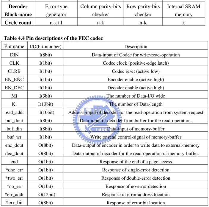
Table 4.4 Pin descriptions of the FEC codec...30
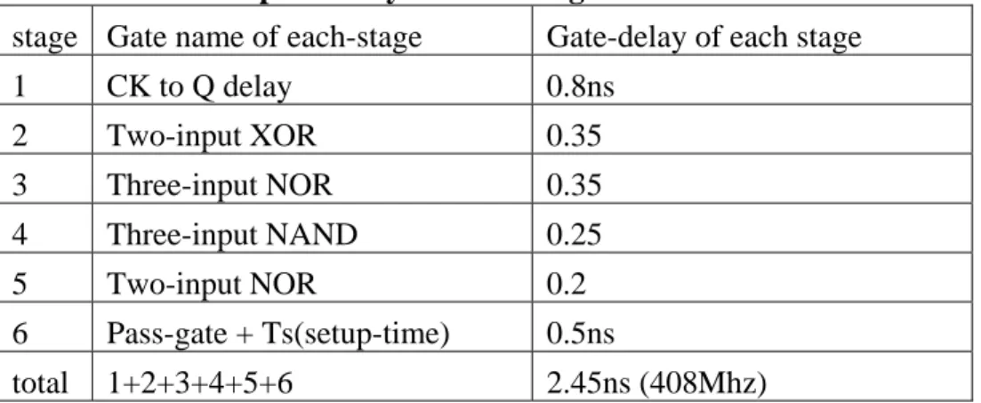
Table 4.5 Critical path delay for each stage...32
Table 4.6 Estimated counts for the proposed FEC-Codec...33
Table 4.7 Comparisons of random-bit errors detecting capabilities and mis-correction...37
Table 4.8 Sector error rate with ECC for different code-length when the sector error rate without ECC is p=10-4...39
Table 4.9 Performance comparisons of different programmable FEC Codec...41
Table 4.10 Advantages and disadvantages between the existing ECC codes and the proposed ECC codes...44
Table 5.1 Simulation results for multiple random-bit errors when the SEC-SoddEC-SBED-DED (N, K, M)=(78, 64, 8) code...53
Table 5.2 Simulation results for multiple random-bit errors on a single-byte when the SEC-SoddEC-SBED-DED (N, K, M)= (78, 64, 8) code...54
Table 5.3 Simulation results for multiple random-bit errors when the SEC-SoddEC-SBED-DED (N, K, M)=(144, 128, 8) code...54
Table 5.4 Simulation results for multiple random-bit errors on a single-byte when the SEC-SoddEC-SBED-DED (N, K, M)= (144, 128, 8) code...54
Table 5.5 Simulation results for multiple random-bit errors when the SEC-SoddEC-SBED-DED (N, K, M)= (76, 64, 4) code...54
Table 5.6 Simulations value and redundancy rate for different information length in figure 5.8...57
Table 5.7 Simulation results for burst-bit errors when the SEC-SoddEC-SBED-DED (N, K, M)= (78, 64, 8) code...58
List of Figures
Fig 1.1 Two different kinds of memory control systems with ECC...2
Fig 2.1 Flash memory reliability problems...4
Fig 2.2 Threshold-voltage distribution of single-bit and multi-bit cell...6
Fig 2.3 Download application-code from external memory to execute application program...8
Fig 3.1 The proposed error correcting code structure for a (m×k) page size...12
Fig 3.2 The construct coding approach has these capabilities as (a)~(d)...14
Fig 3.3 The logical scheme of SEC-SoddEC-SBED-DED code...15
Fig 3.4 Dependence of the user-defined coding-data wide and the number of parity check bits for the proposed Multi-Bit-Layer SEC-SoddEC-SBED-DED code...17
Fig 3.5 Constructed scheme of the proposed (nl, kl, ml, m) Multi-Bit-Layer SEC-SoddEC-SBED-DED code...19
Fig 3.6 Constructed scheme of the proposed (nl =14, kl =8, ml=2, m=4) Multi-Bit-Layer SEC-SoddEC-SBED-DED code...19
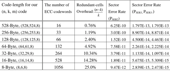
Fig 3.7 The proposed (nl =66, kl =63, ml=8, m=8) SEC-SoddEC-SBED-DED code is used for a 528-bytes page size...21
Fig 3.8 Four (nl =66, kl =63, ml=8, m=8) SEC-SoddEC-SBED-DED code is interleaved over four page memory space...24
Fig 4.1 Block diagram of the proposed programmable ECC Codec...28
Fig 4.2 Schematic of one-bit column parity-check-bit generator...31
Fig 4.3 Schematic of one-pair of row parity-check-bit generator...31
Fig 4.4 An example of encoding procedure of the proposed FEC Codec...32
Fig 4.5 An example of decoding procedure of the proposed FEC Codec...33
Fig 4.6 Design architecture of C-language program for the proposed SEC-SoddEC-SBED-DED Codec...34
Fig 4.7 Dependence of the sector error rate with ECC and redundant-cells overhead for different ECC code-length...40
Fig 5.1 Write flow-chart of memory through ours FEC-Codec...47
Fig 5.3 Encoding timing diagram of FEC-Codec when control parameters (n, k, m) = (259, 256, 8)...49 Fig 5.4 Decoding timing diagram of FEC-Codec when the occurrence of
a single-bit error...50 Fig 5.5 Decoding timing diagram of FEC-Codec when the occurrence of
no error...51 Fig 5.6 Decoding timing diagram of FEC-Codec when the occurrence of
double error...52 Fig 5.7 Error correcting capability comparison for different type of
ECC-codes with K=64...56 Fig 5.8 Error correcting capability comparison for different data-length
Symbol Descriptions
Symbol Meaning
n
Code-length, or the length of an ECC codeword
k information/data/message
length
M, m
Data-I/O wide, or a byte/symbol in bits
r
parity check bit length, or redundant-bit length
N
the number of an ECC codeword bit, where
N =n×mK
the number of Information/data/message bit, where
K =k×mR
the number of redundant-bit/parity check bit, where
R=r×m⎣ ⎦
xlargest integer less than or equal to x
⎡ ⎤
xthe smallest integer greater than or equal to x
+ or ♁
an XOR logic-operation
Keywords and Proper Nouns Explanations
Keywords Meaning
ECC, FEC Error-Correcting-Code, Forward Error-Correcting-Code
MLC
memory
Multi-Level-Cell memory indicate that a 2
qlevel cell has q bits
storage unit
BLC
memory
Binary-Level-Cell memory indicate that a two level cell only
has 1 bits storage unit
MCP
(Stacked) Multi-Chip-Package
MCM
Multi-Chip-Module package
PSRAM
Pseudo Static RAM is equivalent to 1T-SRAM
SDRAM Synchronous Dynamic RAM
FCRAM (Double/Single Data Rate) Fast Cycle RAM
DDR/SDR
SDRAM
Double/Single Data Rate Synchronous Dynamic RAM
SEC-DED Single-Error-Correction─Double-Error-Detection
SBED
Single-Byte-Error-Detection
DEC-TED Double-Error-Correction─Triple-Error-Detection
TEC-QED Triple-Error-Correction─Quadruple-Error-Detection
RS-code
Reed-Solomon Code
BCH-code Bose-Chaudhuri-Hocquenghem Codes
SbEC-DbED
Single b-bit byte Error Correction─Double b-bit byte Error
Detection
SEC-S
oddEC Single-bit Error-Correction─Single odd-bit Error Correction
FEC-Codec Forward Error Correcting Encoder-Decoder
GF(q)
Galois-Field, where q is the order of Galois-Field
BER
Bit Error Rate
FIT
Failure In Time is equivalent to 1-failure per billion
device-hours
Chapter 1
Introduction
1.1 Motivations
Recently, more and more kinds of memory chips are applied to portable devices, such as digital cameras, digital audio and video player, mobile phone, and personal multi-media assistants, etc. In general, many varieties of high capacity memory chips are integrated into a memory card, a multi-chips module package (MCM), a product in package (PIP), or stacked multi-chip package (stacked MCP) for reducing chip-to-chip dimension toward the portable device applications. These varieties of integrated memory-chips modules are almost based on dram and flash memory to organize a specific combo-memory module. Furthermore, more and more the large-capacity memory chips using a deep submicron fabrication process and multi-level cell (MLC, i.e. multiple-bit in a cell unit) device technology is to induce more critical reliability issues, such as disturbs and data retention, and radiation induced soft errors [3]. So the memory control system must guarantee the reliability problems of these varieties of combo memory-modules during the operational life time of memory-chips. Therefore it can be said that memory control system need to adopt some form of error detecting and correcting codes in order to enhance the reliability of memory-chips. In most applications to semiconductor memory systems, errors that occur in semiconductor memory systems can be regarded as either random errors or byte error. The speed of the operations for semiconductor memory systems is very high, and therefore the error-correcting codes (ECC) decoders must be extremely fast. Also the number of redundant overhead cannot be too large [32].
Though many flash and dram memory-chips with on-chip ECC have been presented in the papers [1]-[9], [15]-[19], these ECC-memory chips must pay the access time penalty about 5~25ns and an additional ECC area overhead about 10%~35%. Thus memory-chips with on-chip ECC have high cost and poor performance in access-speed. For the both low-cost and high performance factors of the varieties of integrated memory-chips modules in serial page access operations to compare the figure 1.1 (a) with (b), and figure 1.1 (a), (b) show multiple memory-chips application that the system-level cost of a memory interface controller with ECC like figure (a) may be lower than that figure (b) with ECC-memory chips. In figure 1.1, we know a host memory-controller employ an error correcting code circuits that it will be more efficient to improve the whole memory system performance, reliability and minimize the cost for multiple memory-chips integration.
Therefore memory interface controller built-in ECC will be a better choices as shown in figure 1.1 (a).
Now most of memory-chips have a high speed clock rate or page access-time, such as a 100~200Mhz clock-rate for mobile SDRAM, 200~400Mhz clock-rate for DDR FCRAM, SDRAM, 20ns~40ns page-access PSRAM, 50~100Mhz for page-mode flash. Besides, most of memory-chips have different page or burst-length such as 8bytes~512bytes burst-length for mobile-SDRAM/PSRAM, and specific 264bytes, 528bytes, 2112bytes page-length for
NAND-flash, and different data I/O wide such as 1, 4, 8, 16, 18-bits….etc. So we need a simpler, faster, flexible and programmable error-correcting-coding technology to reach to system-user defined low-cost and high performance demands, and we must also think about the error-correcting-detecting capabilities and parity check-bits overhead.
By the above reasons, for the varieties of integrated memory-chips system, it is needed that the forward error-correcting encoder-decoder can provide a wide programmable coding length, and data-I/O width, minimum decoding latency, acceptable redundancy overhead and
error-correcting-detecting ability, high throughput and high speed encoding-decoding operation with real time mapping-out process.
1.2 Outlines
In chapter 2, the basic concept of dram and flash reliability problems, some key features of error-correcting code for various memory-chips system are described, and the fundamentals of the existing error-correcting code circuits are reviewed briefly.
In chapter 3, the constructed methods and interleaved mechanisms of the proposed SEC-SoddEC-SBED-DED code and Multi-Bit-Layer SEC-SoddEC-SBED-DED
interleaved-codes are clarified for fast and flexible programmable issues due to the different page size of the varieties of memory-chips.
In chapter 4, this section mainly describes hardware implementation for the programmable architecture and circuit design of the proposed FEC codec. Furthermore, the proposed ECC codes have been implemented in C-language software design for any (n, k, m) parameters. In addition, many performances comparisons with the existing ECC also are listed, such as throughput rate (maximum operating transfer rate), complexity (area overhead), decoded error rate...etc.
In chapter 5, the hardware and software simulation results are described, such as encoding-decoding waveform, read-write data flow of the proposed FEC-Codec, decoded error-rate...etc.
Chapter 2
Basic Concepts for Memory Reliability Issues
and the Existing ECC Codes
2.1 The DRAM and Flash memory reliability issues
Firstly, we introduce the common reliability problems to both dram and flash memory. The common reliability problems on flash memory have generally two types of errors [4]: (1) After write and erase cycles, stored electrons can leak away from the floating gate through tunnel oxide during aging. The charge loss causes a decrease in the memory transistor
threshold voltage, which may result in random 0 to1 errors.
(2) During read operation, the floating gate slowly gains electrons with the control gate held at Vcc. The charge gain causes an increase in the memory transistor threshold voltage, which may result in random 1 to 0 errors. The above (1) and (2) reliability problems are shown in Fig. 2.1.
Another reliability problems for dram memories mainly have also two types of errors [5]: (1) One is called the memory cell error-upset that the associated cell or node capacitance in deep submicron process is scale-down, hence the capacitor is highly susceptible to being
discharge by noise electrons.
(2) Another is called bit-line error-upset that the sensing margin of sense amplifier is a very small signals, thus the bit-line differential voltage may degrade due to noise-couple, and hence the resulting read operation may be erroneous.
The foregoing flash and dram reliability will become a significant concern in deep sub-micron MLC (multi-level-cell, a 2q level cell has q bits storage unit) technology. a bi-level single memory cell must distinguish between two voltage states, whereas a multiple-bit MLC-cell uses a voltage window with similar structure size, the distance between adjacent bit-to-bit threshold voltage levels in MLC is much smaller than traditional binary-level memory, which makes the reliability problems of MLC-memories more critical than conventional bi-level cell (BLC) memories [3], [8], as shown in Fig. 2.2 (a), (b).
The most of foregoing reliability issues are caused mainly by soft error due to alpha
particles and soft errors are defined widely such as transient errors, power-supply noise spikes, thermal effects, and man-made states. These errors are called soft, because they do not
damage the physical functions of a cell permanently, and they can easily corrected by complementing the data in the faulty cells [2], [5]. In a DRAM chip more than 98% of single-bit failures are radiation induced soft-errors [20]-[21], and In NAND-flash memory Over 99% of failures are attributed to single-bit soft errors [22]. Because dram storage unit is a trench or stacked capacitor and flash storage unit is by using floating-gate, which is a solid-state memory so the influence of the alpha particle induced soft error rate on dram memory is more significant than flash memory. About DRAM and flash memory reliability testing results are shown in the papers [23]-[27], we can know the average FIT (Failure in Time) and Bit-Error-Rate (BER) under different process, chip-size or different conditions. The soft error rate of different memory-chips is listed as follows [23]-[27], where 1-FIT = 1 failure per billion device-hours.
Type BLC NOR-Flash MLC NOR-Flash BLC NAND-Flash MLC NAND-Flash BLC DRAM # bits 16M/64M 64M 256M 256M ~512M
Process 0.23/0.17um 0.23um 0.16um 0.16um 0.25~0.13um
FITs/Mbit
(Sea Level) 6E-9/3E-6 3E-7
1E-3 (read) 1E-4 (program)
1.0 (read)
1E-2 (program) 500~1000
FITs/Mbit
As a consequence of these issues, the use of error correcting code techniques can help to reach adequate reliability of the deep sub-micron process, high-capacity, MLC-memories for immunity to soft-errors.
2.2 A discussion on the existing ECC codes
Many ECC schemes have been widely proposed to enhance the reliability of
dynamic-RAM, NAND-type flash and solid-state disk [1]-[9], [15]-[19]. In these [1]-[19] papers, it was understood that applying ECC to a memory control system requires a moderate balance between performance (access time penalty, operation frequency, throughput rate, encoding-decoding cycle count, error correcting ability, other features such as interleaving function, etc), chip-size overhead (circuitry complexity and parity check-bit overhead), and reliability enhancement (low decoded error rate or error probability, high detected error rate, soft-error-rate or yield improvement, reducing mean time to failure). Based on the above reasons, the proposed error-correcting code circuit must satisfy the following conditions for the most of various memory chips.
1) For a reliability issue of memory-chips in page-oriented memory-system application, because the memory chips usually can’t have built-in error correcting code circuits
(ECC-circuits) due to the limitations of access time penalty and an additional area cost of ECC-circuits, i.e. the non-ECC commodity memory chips have NAND-type flash and specific mobile-DRAM. So the external memory control systems need a system/board-level ECC to ensure the validity of received data of the page/sector-oriented memories. In
general, memory reliability depends on the both error correcting-detecting capability and the soft-error rate or failure rate of memory-chips.
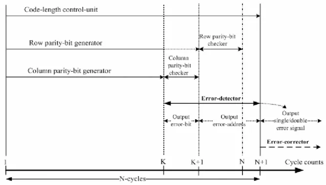
2) For a high throughput data rate, the memory control systems need a high-speed FEC Codec hardware to minimize access latency and maximum operating clock speed. In order to demands of execute in place, the error-correcting code circuit can correct any error-bit of reading random address immediately after serial download program-code procedure from external memory as shown in Fig. 2.3. In other words, after the received n-bytes serial program-code data, the ECC circuit must be to look for the error-address and error-value instantly so that the CPU can execute the program-code right now for real-time application requirements. In general, a high-speed page access time is about 5ns~15ns based on
DDR/SDR SDRAM memory, 10ns~70ns for NOR-Flash, 50ns for NAND-memory. 3) For low-cost considerations as Fig. 1.1. We need a compact, flexible FEC Codec to
minimize the ECC Codec complexity, parity check-bits overhead, and furthermore programmable code-length feature that applied to the different page sizes demands of various memory-chips, i.e. a page or sector in a single memory-chip is organized as m-bits data width (m-bit is one byte length) and an n-bytes data-length, where a page or sector has the number of bits. Programmable (n, k, m) parameters are necessary so that the users of memory-chips can define an arbitrary data length with ECC parity check-bits.
m n×
In general, memory-chip data-wide m is a multiple of 4, such as 4, 8, 16, 32 bits, but some special memories have a specific data-wide. A page length usually is a multiple of 8, such as 8, 16, 32, 64, 128 Bytes, and so on. Furthermore, a page size of NAND-flash is 528, or 2112-Bytes.
Among [1]-[19] literatures, we try to compare these error control code for finding the optimal coding style and to investigate the range of the page-sizes, data-width and an
acceptable Bit-Error-Rate to correspond to the transition error probability of both DRAM and FLASH memories in practical conditions, so that our proposed FEC-Codec has low-cost, low-complexity and high-speed to provide a good performance and moderate reliability meet with the foregoing 1 to 3 ideas. Basically, the existing ECC generation methods have still some restrictions to the programmable coding length and width, and we propose
ECC-generation methods that have almost no restrictions to coding length and width. Here we analyze the existing ECC codes in order to apply for the programmable (n, k, m), where n=code-length, k=data, message or information length, m=data I/O wide or a byte/symbol size in bit. We known parity check-bit lengthr =(n−k), then the number of parity-check
bitsR=(n−k)×m, the number of information-bitsK =k×m, and the total number of coding-bits are N =K +R=n×m(bits). N is user-defined memory block-size with both parity check-bits and information bits equal to a page memory-space, and k >> m in general memory-chips applications.
SEC/SEC-DED Hamming-codes or odd-weight column modified-Hamming-codes were presents in [4], [8], [15], [16] that they are suitable for on-chip, fixed code-length ECC design. It has a proper number of parity-bitsR=
⎡
log2k⎤
+2, and R+K =N for SEC-DED and suits to serial data-bit coding by using a Hamming cyclic-code. It is hard and complex to design a variable code-length n and data-wide m in the modular decoding-circuit unless a multi-SEC-DED code using multiple decoding circuits can solve this problem.However the cost overhead will be obviously increased, i.e. the larger parity check-bits is aboutR=(
⎡
log2k⎤
+2)×m.Another traditional SEC-DED codes are bidirectional cross-parity/product codes that the type of code have been present in [1], [19] for on-chip ECC applications. Though it is suitable for programmable n and m parameters due to a simple encoding-decoding circuit, it also has a large number of parity check bits in proportion to k and m, such asR=k+m+1.
Some DEC-TED codes and TEC-QED codes are presents in [2], [5] and [7] respectively. They have a good correcting capability, and programmable (n, k, m) circuits are feasible, but that’s necessary to pay a largest number of parity check-bits, i.e. the TEC-QED research [7] was designed by combining odd-weight-column SEC-DED with vertical parity bit technique for a memory array, i.e. all word-lines of memory-array are along column direction, bit-lines of array are along row direction. Each column employs odd-weight-column SEC-DED codes, and each row employs a parity bits. So we get a parity check bitsR=m×(log2k+2)+k, or . The DEC-TED researches [2], [5] were designed using
orthogonal Latin-square code which belong a majority-logic decoding code. For a square arrangement of the m m m k R= ×(log2 +2)+ 2
data array, it has also a large parity check-bitR= m3 +1.
The Reed-Solomon code (RS-code), or BCH-code have a powerful multiple bytes error correcting and detecting capability, and a small number of check-bits for single/double byte correction, but have a complex decoding hardware and a longer decoding time. The RS-code
defined in for programmable (n, k, m) are feasible but have some coding limitations
by , , t = the number of error-correcting bytes. In these RS-code researches [9]-[14], the versatility of RS-decoders could be achieved by changing only the information length k with the block length n and symbol size m fixed [10], [11], [14], in order to change the error correcting capability t. Another type is to fix symbol-size m in order to the both n and k are variable [12]-[13]. These architectures pay a largest area cost for decoding circuit, and clock time and decoding latency is also bigger.
) 2 ( m GF 1 2 − = m n r =n−k =2t
A class of multiple bits error correcting and detecting code were presented in [28]-[31] that these codes are based on Fujiwara codes, i.e. An odd-weight-column-matrix code over GF(2b) is an SbEC-DbED code, where b denotes the number of bits in a byte and equal to m. the kinds of code may have arbitrary code and byte length, and the researches have a proper
number of parity check-bits as follows. (3 log ( 2)) 2 1 2 + + = m k R in [28], and
⎡
R m k m mR=log2 + × + −1
⎤
+ in [29], and log⎡
( ) 2 1⎤
11 2 2 × + − − = m− k m R in [30]. The
based-on Fujiwara codes for programmable (n, k, m) are feasible but still pay a complex decoding circuit though these codes have a proper error correcting capability, such as [30] has random double bit within a block error correction- single byte error detecting capability, [29] has single bit error correction-double bit error detection and fixed b-bit byte error detection capability, [28] has t-bit error correction within a single b-bit byte and single b-bit byte error detection capability, where t=3 and b=8, but they still have a poor error detection capability of random double/triple bit failures.
Chapter 3
The Proposed ECC Codes Constructed
Methods and Interleaved Mechanisms
3.1 Constructed method of the proposed SEC-S
oddEC-SBED-DED
ECC code
We propose a systematic error-correcting code by modified bidirectional cross-parity code which called SEC-SoddEC-SBED-DED codes to have the kinds of capabilities, such as
random Single bit Error Correction-Single odd-bit Error Correction within a single byte-
Single Byte Error Detection-random Double bits Error Detection. Traditional bidirectional
cross-parity/product SEC-DED codes need parity check-bits r=k+m+1, that we utilize hierarchical structure to reduce the number of parity check bit. The proposed (n, k, m) systematic code is constructed as shown Fig. 3.1, and the following steps are performed: Step1: To define an encoded data page or sector size asm×kbits for m-bit data wide and the
information length k, where0≤i≤m−1, and0≤ j≤k−1.
Step2: Each i-column is to perform a vertical-direction parity-bit for all bits.
This will result in generating m-bit column-parity-bits as the expression:
where addition is equal to XOR logic-operation and b
1 0≤ j≤k−
∑
− = = 1 0 k j ij i b C ij indicatescoordinate of one bit position.
Step3: Each row is to perform horizontal-direction parity bits using a hierarchical method for these m-bit bytes of k rows. This will result in generating (2×
⎡
log2k⎤
) rowparity-bits. These parity check-bit generating expression is as follows.
∑
for ,i.e. (j mod 2)=1, and for− = = 1 0 1 m i ij b R j=odd
∑
− = = 1 0 1' m i ij bR j=even,i.e. (j mod 2)= 0.
∑
− = = 1 0 2 m i ij bR for ( j mod 4) = 2 or 3, and
∑
for ( j mod 4) = 0 or 1.− = = 1 0 2' m i ij b R
∑
− = = 1 0 3 m i ij bR for ( j mod 8) = 4,5,6, or 7, and
∑
for ( j mod 8) = 0,1,2 or 3.− = = 1 0 3' m i ij b R
If j=0, 1, 2….k-1, let is the number of a pair of row parity-bits,
then for ( j mod ) = 0 ~ (
⎡
k x= log2⎤
∑
− = = 1 0 ' m i ij X b R 2X 2(X−1) −1), and∑
for ( j mod ) = ~ ( − = = 1 0 m i ij X b R 2X 2(X−1) 2X −1), where mod≣modulo-operator. Hence we can utilizex=1~⎡
log2k⎤
to compute all pairs of row parity-bits.Step4: By the step1 to step3, we can get the total parity check bit: for a
data page size of bits, hence the bits number of code-length n = k (the number
of data-bits) + r (the number of parity check-bits) =
⎡
log⎤
) 2 ( × 2k +m ) (m×k⎡
log⎤
) 2 ( ) (k×m + × 2k +m bits.If m-bit data-wide usually represents a byte wide, let n = +(2×
⎡
log2⎤
+1)m k
k bytes.
In a write operation, firstly we write k data-bytes to external-memory in sequence, and then the encoded r parity check-bytes by step1~step3 continue to write in
memory after k data-bytes, in order to finish the proposed systematic error-correcting-code. Hence a serial access operation, it just
needsn=k+rclock-cycle counts.
the encoded r parity check-bytes by step1~step3 will gain new column parity check-bits
for and new row parity check pair-bits for
i
C
1
0≤i≤m− (RX,R'X ) 1≤x≤
⎡
log2k⎤
after the received k data-bytes. The decoding process is as following steps.Step5: Syndrome generation methods are expressed as follows.
During the 0~(k-1) cycles for reading information bytes, and this k-th cycle for reading old column parity check-byte, and (k+1)~(n-1) cycles for reading old row parity check-bytes, so that we generate column syndrome bits at k-th cycle, and row syndrome bits during (k+1)~(n-1) cycles as the following expression:
Letbikindicates one bit position of old column parity check-byte on the read k-th byte
for0≤i≤m−1. Here addition is equal to an XOR logic-operation. Column syndrome-bits:Scol(i)=bik +Ci
Letbijindicates one bit position of old row parity check-byte for(k+1)≤ j≤(n−1),
1
0≤i≤m− , and1≤x≤
⎡
log2k⎤
.Row syndrome-bits: X , for i= odd integer. m i ij row x b R S =
∑
+ − = 1 1 ) (X, for i= even integer. m i ij row x b R S' ( ) ' 1 0 + =
∑
− =Step6: Error correcting and detecting methods are analyzed as follows.
(a) No error: allScol(i)=Srow(x)=S'row(x)=0, for0≤i≤m−1, and1≤x≤
⎡
log2k⎤
. Another type of error is that it has a single bit error falling in the ECC-area, and weassume that it’s no error occurring in information-area when the three results has only 1 bit equal to logic-1.
) ( ' ), ( ), (i S x S x
Scol row row
(b) SEC-SoddEC: there are odd-bit errors occurring on a single-byte that these error-bits
can be corrected. When the both , and for
are existence, where indicate error-bits position as an error
value and indicate error-address as an error location. We know the error
value and error location that we can invert the error-bit data in order to correct it when the error address is read.
∑
− = = = 1 0 1 ) ( m i i col i S {Srow(x)+S'row(x)}=1⎡
k x log2 1≤ ≤⎤
Scol(i) ) (x Srow(c) SBED: if (a), (b) are inexistence, but
∑
and− = = = 1 0 0 ) ( m i i col i S Srow(x)=S'row(x)=0
for0≤ x≤
⎡
log2k⎤
, indicate that a single-byte error at least are detected. In the other words, there are some even-bits errors occurring in a single-byte or multiple-bytes.(d) DED: The type of error is assumed that it has the case of double errors or larger than double errors. If (a), (b), (c) are inexistence, then anyScol(i)≠0,Srow(x)≠0 or
0 ) ( ' x ≠
Srow indicates at least a double error existence.
The above (a), (b) both may be correctable, and the both (c) and (d) may be detectable and not to be correctable.
The foregoing error correcting code generation methods are very suitable for software or hardware implementation, programmable (n, k, m) ECC especially. By the above constructed method, we present a low-complexity and high-speed hardware in chapter 4.
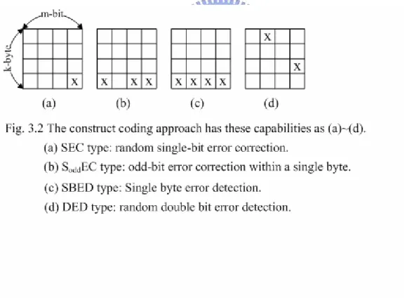
Fig. 3.2 shows four capabilities of the proposed code for the16-bits memory page-size of information length k=4, and data wide m=4. The “X” denotes one fail-bit position.
Fig. 3.3 shows logical-scheme of the SEC-SoddEC-SBED-DED code for the16-bits memory
page-size of information length k=4, and data wide m=4. We can generate the parity check-bits by the foregoing step1~3.
3.2 Constructed methods of Multi Bit-Layer SEC-S
oddEC-SBED-DED
ECC code
Most interleaved techniques mainly can be used to solve the burst errors problems [32], and error patterns involving two or more adjacent cells are generally recovered by a proper
physical interleaving of cells belong to the same codeword, thereby increasing overall memory reliability [18]. Some multi-SEC/DED codes are interleaved for each word-line of on-chip ECC or each data I/O of off-chip ECC are presented in [3], [4], [7], [16], [18]. The papers [3], [18] present an on-chip ECC scheme for MLC-flash memories, based on a binary code providing single-bit correction, are organized in different bit-layer. The paper [4] is a (522,512) SEC hamming cyclic code for each data I/O, that this multi-ECC (n, k) codes are optimized in consideration of balance between the reliability improvement and
redundant-cells area overhead, but its weakness is that has a fixed 2n decoding latency even if the data is no error. The paper [7] is a TEC-QED ECC code which was designed by
combining odd-weight-column SEC-DED hamming-code with the vertical parity bit
techniques, but it has a large redundant cell overhead as parity-check bit .
The paper [16] is a multi SEC-DED (n, k) Hamming code that a k-bit information data was
k k m
split up into two SEC-DED hamming codeword so that it able to correct a two-bit error in two-bits-per-cell MLC-DRAM. The foregoing paper [3], [7],[16], [18] are only suitable to specific on-chip ECC coding way, and in practical, we need a compact, flexible and quick interleaved coding method in order to reach programmable coding and real-time mapping-out operation. So we propose an interleaved method which is called Multi-Bit-Layer
SEC-SoddEC-SBED-DED code. The principle of the proposed interleaved-code is to encode a
-bits block-data, and generate respective SEC-S )
(k×m (nl,kl,ml) oddEC-SBED-DED code on
each data I/O so m-bit data I/O perform m-number of(nl,kl,ml)SEC-SoddEC-SBED-DED
code which is called(nl,kl,ml,m)Multi-Bit-Layer SEC-SoddEC-SBED-DED code.
For a programmable(nl,kl,ml,m)Multi-Bit-Layer SEC-SoddEC-SBED-DED code, each
data I/O code-length has nl-bytes, the user-defined coding-data wideon each data-I/O has ml-bit, the number of data I/O wide is m-bit, and the encoded information length on each
data-I/O has also kl-bytes correspond to ⎥
⎥ ⎤ ⎢ ⎢ ⎡ + = l l m R k
n , where R is the number of parity check
bits on each data-I/O equals(2 log2 l)
l m m k + ⎥ ⎥ ⎥ ⎤ ⎢ ⎢ ⎢ ⎡ ⎟⎟ ⎠ ⎞ ⎜⎜ ⎝ ⎛ × -bit, and l l m k k = must be an integer. When m=1 (only one data I/O), and k is equal to 64-bit, 512bit, 4096-bit respectively, the dependence of user-defined coding-data wide ml and the number of parity check bit R is
shown in Fig. 3.4.
For a Multi-Bit-Layer SEC-SoddEC-SBED-DED code, if the number of data I/O wide is m, the
number of information-length is k and the number of total information-bit is k×m, then the
total number of parity check bit is
( )
⎡
k⎤
m m m m m k R l l l l × + × = × + ⎥ ⎥ ⎥ ⎤ ⎢ ⎢ ⎢ ⎡ ⎟⎟ ⎠ ⎞ ⎜⎜ ⎝ ⎛ ×The above(nl,kl,ml,m)Multi-Bit-Layer SEC-SoddEC-SBED-DED code can be constructed as
shown in figure 3.5, and the generating method is described as following steps.
Step1: To define an encoded data page or sector size asm×kbits for m-bit data wide and the information length k, the user-defined coding-data wideon each data-I/O has ml-bit,
Firstly let0≤i≤m−1,0≤ j≤k−1, and0≤h≤ml −1 in order to construct multi-bit-layer ECC code, and we can gain
l l m k k = =integer, ) log 2 ( 2 l l m m k R + ⎥ ⎥ ⎥ ⎤ ⎢ ⎢ ⎢ ⎡ ⎟⎟ ⎠ ⎞ ⎜⎜ ⎝ ⎛ × = , ⎥ ⎥ ⎤ ⎢ ⎢ ⎡ + = l l m R k
n on each data-I/O. Thus each data I/O is to
perform a single(nl,kl,ml)Bit-Layer SEC-SoddEC-SBED-DED code, total data-I/O
number is m-bit to perform a(nl,kl,ml,m)Multi-Bit-Layer SEC-SoddEC-SBED-DED
code.
Step2: Each data I/O is to perform column-parity check-bits and row-parity check-bits, where the number of column-parity check-bits equal to ml-bits and the number of row-parity
variable for0≤ j≤k−1, and0≤h≤ml −1.
Hence each data I/O generate ml -bit column parity bits as the expression:
if and only if ( j mod m
j i h i b
C, =⊕ , l = h).
Each data I/O generate row parity bits as the expression:
j i i b R,1 =⊕ , iff ( ⎥ ⎦ ⎥ ⎢ ⎣ ⎢ l m j
mod 2)=1, andRi',1 =⊕bi,j iff ( ⎥
⎦ ⎥ ⎢ ⎣ ⎢ l m j mod 2)= 0. j i i b R,2 =⊕ , iff ( ⎥ ⎦ ⎥ ⎢ ⎣ ⎢ l m j
mod 4) = 2 or 3, and Ri',2 =⊕bi,j iff ( ⎥
⎦ ⎥ ⎢ ⎣ ⎢ l m j mod 4) = 0 or 1.
As the same computing form, we can continue to prove the formula:
If j is a variable equal to 0, 1, 2…till k-1, let
⎡
( )
ll k m k X log2 = log2 ⎥ ⎥ ⎥ ⎤ ⎢ ⎢ ⎢ ⎡ ⎟⎟ ⎠ ⎞ ⎜⎜ ⎝ ⎛ =
⎤
is thenumber of a pair of row parity-bits, thenRi',X =⊕bi,j iff ( ⎥
⎦ ⎥ ⎢ ⎣ ⎢ l m j mod ) = 0 ~ ( 2 ), and iff ( X 2 1 ) 1 (X− − j i X i b R, =⊕ , ⎥ ⎦ ⎥ ⎢ ⎣ ⎢ l m j
mod ) = ~ ( ), where mod≣
modulo-operator, the sign ♁ equals to an XOR logic-operation, denotes the
largest integer less than or equal to x, and X
2 2(X−1) 2X −1
⎣ ⎦
x⎡ ⎤
x denotes the smallest integer greater thanor equal to x.
Step3: By the above step1 and step2, them×kblock-data is encoded intom×n=m×(k+R) multi-bit-layer ECC code, and we can generate the parity-check bit on each data I/O:
( )
⎡
l⎤
l l l m k m m k R + = × + ⎥ ⎥ ⎥ ⎤ ⎢ ⎢ ⎢ ⎡ ⎟⎟ ⎠ ⎞ ⎜⎜ ⎝ ⎛ ×=2 log2 2 log2 (bits).
Total parity-check-bit overhead isR×m=(2×
⎡
log2( )
kl⎤
+ml)×m (bit).Thus an overall encoded page size equals to (k×m)+(2×
⎡
log2( )
kl⎤
+ml)×m (bits). An example of logical scheme is shown in Fig. 3.6, and the logical expressions of parity check-bits are also list in figure 3.6 by using the above step1~tep3.In the figure 3.6, we know a (14, 8, 2, 4) Multi-Bit-Layer SEC-SoddEC-SBED-DED code has
2-bit column-parity-check-bit, and 4-bit row-parity-check-bit on each data-I/O to encode an information area(k× m)=(8×4)-bit into an ECC-codeword(nl×m)=(12×4)bit.
) , , ,
(nl kl ml m Multi-Bit-Layer SEC-SoddEC-SBED-DED code owns the capability of
Single-Byte Error Correction-Odd-bytes Error Correction within consecutive bytes-
consecutive Bytes Error Detection-random Double bits Error Detection on each data-I/O. l
m
l
m
Because of the constructed method of Multi-Bit-Layer SEC-SoddEC-SBED-DED code has the
simpler and faster generation steps, hence this interleaved code can be implemented in a compact and high-speed hardware circuit, and it has a very large programmable
range. ) , , , (nl kl ml m
3.3 Application Examples of Interleaved Mechanisms using Multi-Bit-Layer
SEC-S
oddEC-SBED-DED code
Many types of interleaved methods using the proposed code can apply to different page size for various memory-chips system. Here we utilize Multi-Bit-Layer SEC-SoddEC-SBED
-DED codes to form two interleaved-code mechanisms, which are mainly applied to the NAND-type flash memory that its memory array consists of many pages unit. A page size equals 528-bytes which is used to page-program or page-read operation, and a block size are 32 pages which is used to block-erase operation.
The first interleaved method using Multi-Bit-Layer SEC-SoddEC-SBED-DED code is
described as follows:
Basically, the conventional multiple ECC codes utilize the proposed (n, k, m)=(66, 63, 8) SEC-SoddEC-SBED-DED code to let a 528-bytes page-size is divided into 8 segments, and
every segment has 63 data-bytes and additional 3 parity check bytes. The conventional multiple ECC codes organization are shown in Fig. 3.7 (a), and every segment has only the default error-correcting and detecting capability of SEC-SoddEC-SBED-DED code, therefore
it can not correcting single-byte error or detection double-byte errors. For improving this weakness of the conventional multiple ECC code, we may utilize the foregoing interleaved code in section 3.2 that the =(66, 63, 8, 8) Multi-Bit-Layer
SEC-S ) , , , (nl kl ml m
oddEC-SBED-DED coding method to let this interleaved code is capable of Single-Byte
Error Correction-Odd-bytes Error Correction within eight consecutive bytes-Eight
consecutive Bytes Error Detection-random Double bits Error Detection on each data I/O as
shown in Fig. 3.7 (b). According to figure 3.7 (a) and (b), we know segment-1 has 63 data-bytes from , until , and 3 parity check-bytes from to , where each
denotes a data byte position, each denotes a parity check-byte position, m=data
wide=segment number for , and k=the information length for . Every segment stores 63 data-bytes with 3 parity check-bytes on each horizontal row-direction as figure 3.7 (a), so we change the arrangement of 66-bytes codeword to let 66-bytes(528-bits) lie on each vertical column-position in sequence as figure 3.7 (b). An n-bytes (n×m bits)
codeword is stored in the same bit-layer data-I/O, i.e. the segement-1 codeword is stored in the first bit-layer data-I/O of the 528-bits (b
0 , 1 D D1,1 D1,62 C1,0 C1,2 Dm,k k m C , 8 1≤ m≤ 0≤ k≤62
0,0~ b0,511) memory space, the segement-2
and so on. Therefore the above way can create a =(66, 63, 8, 8) Multi-Bit-Layer SEC-S ) , , , (nl kl ml m oddEC-SBED-DED code to fit into a 528-bytes page size.
For a specific page size like shown in figure 3.7(b), we can construct the (66, 63, 8, 8) Multi-Bit-Layer SEC-SoddEC-SBED-DED coding mechanism within a single-page by using
section 3.2 constructing methods is described as following steps.
Step1: We have known a page size equal ton×m=528×8-bit. Letm=ml,
l l
m n
n = =integer, then a page has m number of bit-layer ECC-codeword, and each ECC-codeword is
said that l l m m n R + ⎥ ⎥ ⎥ ⎤ ⎢ ⎢ ⎢ ⎡ ⎟⎟ ⎠ ⎞ ⎜⎜ ⎝ ⎛ × = 2
max 2 log (bits), ⎥
⎦ ⎥ ⎢ ⎣ ⎢ − = l l m R n k max (bytes), k =kl ×ml
(bits), and the realR=2×
⎡
log2( )
kl⎤
+ml (bits), and ⎥ ⎥ ⎤ ⎢ ⎢ ⎡ + = = l l l l m R k m n n (bytes).By the above descriptions, we can solve the values: When n=528,m=ml =8,then 66 , 20 , 504 , 63 = = = = l l k R n k .
Step2: Each data I/O is to perform an ECC-codeword with column-parity check-bits and row-parity check-bits. The number of column-parity check-bits is equal to ml-bits.
Let i=0, 1, till (m-1), and j is a variable for0≤ j ≤k−1.
Thus each data I/O generate 8-bit column parity bits as the expression: if and only if ( j mod 8 = 0);
j i i b
C,0 =⊕ , Ci,1 =⊕bi,j if and only if ( j mod 8 = 1);
j i i b
C,2 =⊕ , if and only if ( j mod 8 = 2);Ci,3 =⊕bi,j if and only if ( j mod 8 = 3);
j i i b
C,4 =⊕ , if and only if ( j mod 8 = 4);Ci,5 =⊕bi,j if and only if ( j mod 8 = 5);
j i i b
C,6 =⊕ , if and only if ( j mod 8 = 6);Ci,7 =⊕bi,j if and only if ( j mod 8 = 7);
Each data I/O generate row parity bits as the expression:
j i i b R,1 =⊕ , iff ( ⎥⎦ ⎥ ⎢⎣ ⎢ 8 j
mod 2)=1, andRi',1 =⊕bi,j iff ( ⎥⎦ ⎥ ⎢⎣ ⎢ 8 j mod 2)= 0. j i i b R,2 =⊕ , iff (⎢⎣⎢ ⎥⎦⎥ 8 j
mod 4) = 2 or 3, and Ri',2 =⊕bi,j iff (⎢⎣⎢ ⎥⎦⎥ 8
j
mod 4) = 0 or 1.
As the same computing form, we can continue to prove the formula:
If j is a variable equal to 0, 1, 2…till k-1, letX =
⎡
log2( )
kl⎤
=6 is the number of a pair of row parity-bits, thenRi',6 =⊕bi,j iff (⎥⎦ ⎥ ⎢⎣ ⎢ 8 j mod ) = 0 ~ ( ), and iff ( 6 2 25 −1 j i i b R,6 =⊕ , ⎢⎣⎢ ⎥⎦⎥ 8 j
mod26) =25~ (26 − ), where mod≣modulo-operator, the sign 1 ♁ equals to an XOR logic-operation,
⎣ ⎦
x denotes the largest integer less than or equalto x, and
⎡ ⎤
x denotes the smallest integer greater than or equal to x.Step3: By the above step1 and step2, we can generate the parity-check bit on each data I/O: R= 20-bits, total parity-check-bit overhead isR× m=160-bits and an overall encoded page size equals(kl ×ml +R)×m=(k+R)×m=524×8-bit. So we must make sure that
the overall encoded page size is smaller than a page sizen×m=528×8-bit.
The result is that an interleaved(nl,kl,ml =m)SEC-SoddEC-SBED-DED code for a
single page-size owns the capability of Single-Byte Error Correction-Odd-bytes
Error Correction within m consecutive bytes-m consecutive Bytes Error Detection-
random Double bits Error Detection on each data I/O. )
(n×m
The second interleaved method using Multi-Bit-Layer SEC-SoddEC-SBED-DED code is
described as follows:
Furthermore, we can continue to expand the error-correcting and detecting capable of an interleaved (66, 63, 8, 8) SEC-SoddEC-SBED-DED code for four consecutive pages that this
code owns these capability of four consecutive Bytes Error Correction-Odd-bytes Error
Correction within (8×4) consecutive bytes-(8×4) consecutive Byte Error Detection-four
random Double bits Error Detection on each data I/O. The skill is shown in Fig. 3.8,
where indicates a data bit position, f= page number from 0 to 3, i=data wide=segment
number from 0 to 7, j=the bit number of each segment from 0 to 2015. The segment of each page has 63 data-bytes equal to 504-bits length and 3 parity-check bytes equal to 24-bits length that we expand the overall interleaved codeword over four pages, e.g., the four-bits
, , , are included in the first group, where the first-bit is as the first
data-bit of segment-1 in page1, the second-bit is as the first data-bit of segment-1 in
page2, the third-bit is as the first data-bit of segment-1 in page3, the fourth-bit is
as the first data-bit of segment-1 in page4, respectively. Therefore a four page has (63×8)=504 groups as 2016-bits data-length on each segment, it implies that every column or each
segment has four (66, 63, 8, 8) SEC-S j i f b ,, 0 , 0 , 1 b b2,0,1 b3,0,2 b4,0,3 b1,0,0 1 , 0 , 2 b 2 , 0 , 3 b b4,0,3
oddEC-SBED-DED interleaved code over four
Thus the specific consecutive-pages like shown in figure 3.8, we can construct the
interleaved(nl,kl,ml,m)Multi-Bit-Layer SEC-SoddEC-SBED-DED coding mechanism over l-page is described as following steps.
Step1: We have known a page size is equal to(n×m)-bits, and need to encode l
consecutive-pages. A single page has m number of bit-layer ECC-codeword, and each
ECC-codeword is said that l
l m m n R + ⎥ ⎥ ⎥ ⎤ ⎢ ⎢ ⎢ ⎡ ⎟⎟ ⎠ ⎞ ⎜⎜ ⎝ ⎛ × = 2
max 2 log (bits), ⎥
⎦ ⎥ ⎢ ⎣ ⎢ − = l l m R n k max
(bytes), k =kl ×ml (bits), and the realR=2×
⎡
log2( )
kl⎤
+ml (bits), and⎥ ⎥ ⎤ ⎢ ⎢ ⎡ + = = l l l l m R k m n
n (bytes). The denotes the bit position of each data-I/O over
l-page, where f denotes the number of page for j i f b ,,
1
0≤ f ≤l− , i denotes the number of data-I/O for , j denotes the number of the encoded information length over
l-page for 1 0≤i≤m− 1 ) ( 0≤ j≤ k×l − .
Step2: Each data I/O is to perform the interleaved ECC-codeword over l-page, the number of column-parity check-bits is equal to(ml × bits, and the number of row-parity l)
check-bits is equal to{(2×
⎡
log2( )
kl⎤
)×l}bits.Let i=0~(m-1), f=0~(l−1), and the both j, h are variable for0≤ j≤(k×l)−1, .
Hence each data I/O generate column parity bits as the expression: if and only if { j mod
1 0≤h≤ml − j i f b Cf,i,h =⊕ ,, (ml ×l)=(h×l+ f)}.
For example as shown in figure 3.8, the first data-I/O is to perform the interleaved ECC-codeword over 4-page, the number of column-parity check-bits is equal to(ml × l)=8×4=32bits. Therefore we know0≤ j≤2015,0≤ h≤7 then
j
h b
C0,0, =⊕ 0,0, if and only if { j mod32= h( ×4)},
j
h b
C1,0, =⊕ 1,0, if and only if { j mod32= h( ×4+1)},
j
h b
C2,0, =⊕ 2,0, if and only if { j mod32= h( ×4+2)},
j
h b
C3,0, =⊕ 3,0, if and only if { j mod32= h( ×4+3)}.
Each data I/O generate row parity bits as the expression:
j i f b Rf,i,1 =⊕ ,, iff ( ⎥ ⎦ ⎥ ⎢ ⎣ ⎢ × l m j l
mod 2)=1, andRf',i,1 =⊕bf,i,j iff ( ⎥
⎦ ⎥ ⎢ ⎣ ⎢ × l m j l mod 2)= 0. j i f b Rf,i,2 =⊕ , , iff ( ⎥ ⎦ ⎥ ⎢ ⎣ ⎢ × l m j l
mod 4) = 2 or 3, andR'f,i,2 =⊕bf,i,j iff ( ⎥
⎦ ⎥ ⎢ ⎣ ⎢ × l m j l mod
4) = 0 or 1. As the same computing form, we can continue to prove the formula:
Let
⎡
( )
l l k m k X log2 = log2 ⎥ ⎥ ⎥ ⎤ ⎢ ⎢ ⎢ ⎡ ⎟⎟ ⎠ ⎞ ⎜⎜ ⎝ ⎛=
⎤
is the number of a pair of row parity-bits,thenR'f,i,X =⊕bf,i,j iff ( ⎥ ⎦ ⎥ ⎢ ⎣ ⎢ × l m j l mod2X ) = 0 ~ (2(X−1) −1), and iff ( j i f b Rf,i,X =⊕ ,, ⎥ ⎦ ⎥ ⎢ ⎣ ⎢ × l m j l mod2X ) =2(X−1)~ (2X −1).
For example as shown in figure 3.8, the first data-I/O is to perform the interleaved ECC-codeword over 4-page, the number of row-parity check-bits is equal
parity-bitsX =
⎡
log2( )
kl⎤
=6. When0≤ j≤2015,0≤ h≤7, and f=1, we know that iff ( j b R0,0,1 =⊕ 0,0, ⎥⎦ ⎥ ⎢⎣ ⎢ 32 jmod 2)=1, andR0',0,1 =⊕b0,0,j iff ( ⎥⎦ ⎥ ⎢⎣ ⎢ 32 j mod 2)= 0,
and ,…., till iff (
2 , 0 , 0 R ' 2 , 0 , 0 R R0,0,6 =⊕b0,0,j ⎢⎣⎢ ⎥⎦⎥ 32 j mod ) = ~ ( ), and iff ( 6 2 25 26 −1 j b R0',0,6 =⊕ 0,0, ⎢⎣⎢ ⎥⎦⎥ 32 j mod26) = 0 ~ (25 − ). 1
Step3: By the above step1 and step2, we can generate the parity-check bit of each data-I/O over l-page:R=(2×
⎡
log2( )
kl⎤
+ml)×l (bits).Total parity-check-bit overhead over l-page isR=(2×
⎡
log2( )
kl⎤
+ml)×l×m (bit). Thus an overall encoded page size is equal to{
k+(2×⎡
log2( )
kl⎤
+ml)×l}
×m (bits).Therefore, the consequence is that a(n×m)page-size and l-consecutive-pages using an interleaved(nl,kl,ml)SEC-SoddEC-SBED-DED code which owns the capability ofl-Byte
Error Correction-Odd-bytes Error Correction within(l×ml)consecutive bytes-
consecutive Bytes Error Detection-l-random Double bits Error Detection on each
data I/O. ) (l×ml
Chapter 4
Programmable Architecture, Circuit and
Software Program Design for the proposed
FEC Codec
4.1 Programmable architecture of the proposed FEC Codec
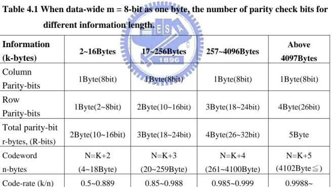
For a various page or sector size to different memory-chips, The proposed error-correcting methods are designed into a programmable encoder-decoder for (n, k, m)= (4100~4, 4096~2, 8~1), where information-length k may be changed from 2, 3 or 4, until 4096-bytes and m may be changed from 1, 2, or 3 until 8-bits, and n=k+rin byte notation, or
in bit notation as shown in table 4.1. m r m k m n× = × + ×
Table 4.1 When data-wide m = 8-bit as one byte, the number of parity check bits for different information length.
Information
(k-bytes) 2~16Bytes 17~256Bytes 257~4096Bytes
Above 4097Bytes Column
Parity-bits 1Byte(8bit) 1Byte(8bit) 1Byte(8bit) 1Byte(8bit) Row
Parity-bits 1Byte(2~8bit) 2Byte(10~16bit) 3Byte(18~24bit) 4Byte(26bit) Total parity-bit
r-bytes, (R-bits) 2Byte(10~16bit) 3Byte(18~24bit) 4Byte(26~32bit) 5Byte Codeword n-bytes N=K+2 (4~18Byte) N=K+3 (20~259Byte) N=K+4 (261~4100Byte) N=K+5 (4102Byte≦) Code-rate (k/n) 0.5~0.889 0.85~0.988 0.985~0.999 0.9988~
The block diagrams of the proposed programmable encoder-decoder architectures are shown in Fig. 4.1. These functional sub-blocks are described as follows.
4.1.1 Sub-block Functions of Encoder
Column parity-bits generator: By the foregoing step2, this generator uses XOR-operation from the first data-bit of data-width to the final data-bit of data-width that the results of XOR-operation store in m column parity-bit registers, where m=1~8bit is decided by 3-bit value ofmias below.
Mi (setup of data wide) 000/b 001/b 010/b 011/b 100/b 101/b 110/b 111/b m (data-I/O wide) 1-bit 2-bit 3-bit 4-bit 5-bit 6-bit 7-bit 8-bit
Row parity-bits generator: By the foregoing step3, this generator also uses XOR-operation from the first data byte of page-length to the final data-byte of page-length that the results of XOR-operation store in x-pairs of row parity-bit registers, wherex=
⎡
log2k⎤
is decided by 13-bit value ofkias below.Ki (setup of data length) 0~1/h 2/h 3/h 4/h … 0fff/h 1000/h above k (data-byte length) unused 2B 3B 4B … 4095B 4096B unused
Code-length control unit: It may setup the different page-sizes from 2-bytes to 4096-bytes that it consists of Code-Length Address Counter and Code-Length Comparator.
![Table 4.7 Comparisons of random-bit errors detecting capabilities and mis-correction ECC-codes [28] [29] [30],[31] [32] ours ECC-code capability S 3/8 EC-S 8 ED, For (76,64) and (141,128) code](https://thumb-ap.123doks.com/thumbv2/9libinfo/8464915.183318/48.892.120.839.152.902/table-comparisons-random-errors-detecting-capabilities-correction-capability.webp)
![Table 4.9 Performance comparisons of different programmable FEC Codec Reference papers [4] [6] [35] ECC-Code type <note 1> Multi-bit-layer SEC Hamming-code, A fixed (N,K,M)=(522, 512,8) codec RS-code, A fixed (n, k, m)=(72,64,8) decoder](https://thumb-ap.123doks.com/thumbv2/9libinfo/8464915.183318/52.892.118.805.106.840/performance-comparisons-different-programmable-reference-multi-hamming-decoder.webp)
![Table 4.9 (To be continued) Reference papers [12] [13] [10] ECC-Code type RS-code, A programmable (n, k, m)=(255, 239, 8) decoder for n=255~13, t=1~10,m=8 RS-code, A programmable (n, k, m)= (255, 239, 8) decoder for 8t8,m1,2n=m−≤≤ RS-code, A pr](https://thumb-ap.123doks.com/thumbv2/9libinfo/8464915.183318/53.892.115.806.113.819/table-continued-reference-papers-programmable-decoder-programmable-decoder.webp)
