用低壓元件實現之混合電壓共容
石英振盪電路設計
學生: 廖 宏 泰 指導教授: 柯 明 道 教授
國立交通大學
電子工程學系 電子研究所碩士班
ABSTRACT (CHINESE)
摘要
隨著互補式金氧半(CMOS)製程技術進步至奈米尺寸(Nanometer-Scale), 為了要在一個較低的供應電壓(1xVDD)下能提供更快的操作速度,閘極氧化 層的厚度也必須跟著下降,然而在電路板上的電壓準位為了能相容於較早期的微 電子系統介面規格,有可能還維持在較高的電壓準位(2xVDD 或是更高),所以 針對此種混合電壓共容應用的輸入輸出介面電路設計上,則要考量閘極氧化層可 靠度(Gate-Oxide Reliability)、熱載子衰退效應(Hot-Carrier Degradation)以及 漏電流(Leakage Current)等的問題。在本篇論文中,提出了三種混合電壓介面電路,第一個電路是使用閘極電 壓追隨電路(Gate-Tracking Circuit)以及動態 N 型井偏壓電路(Dynamic N-Well Bias Circuit)實現之混合電壓輸入輸出緩衝器(Mixed-Voltage I/O Buffer),目的 是為了改善之前的混合電壓輸入輸出介面電路的一些問題,第二個電路是新提出 的混合電壓石英振盪電路一,第三個電路是新提出的混合電壓石英振盪電路二, 上述所提之三個電路皆以低壓元件實現之,且成功克服在混合電壓介面下的閘極 氧化層可靠度問題。上述所提之三個混合電壓介面電路皆已在1.2 伏 0.13 微米互 補式金氧半製程裡實現,用以操作在 1.2/2.5 伏的混合電壓介面下;並且針對第 二及第三個新提出的混合電壓石英振盪電路,又另外實現在1 伏 90 奈米互補式 金氧半製程中,用以操作在1/1.8 伏的混合電壓介面。
Circuit Design of Crystal Oscillator in
Mixed-Voltage-Tolerant I/O Interfaces with
Low-Voltage Devices
Student: Hung-Tai Liao Advisor: Prof. Ming-Dou Ker
Department of Electronics Engineering & Institute of Electronics
National Chiao-Tung University
ABSTRACT (ENGLISH)
ABSTRACT
In the nanometer-scale CMOS technology, the gate-oxide thickness has been scaled down to support a higher operating speed under a lower power supply (1xVDD). However, the board-level voltage levels could be still in a higher voltage levels (2xVDD, or even more) for compatible to some earlier interface specifications in a microelectronics system. The I/O interface circuits have been designed with considerations on the gate-oxide reliability, leakage current and hot-carrier degradation in such mixed-voltage applications.
In this thesis, three kinds of mixed-voltage interface circuits are presented, The first is the mixed-voltage I/O buffer with gate-tracking circuit and dynamic n-well bias circuit for improving some drawbacks of the prior ones, the second is the new proposed mixed-voltage crystal oscillator circuit Ⅰ and the third is the new proposed mixed-voltage crystal oscillator circuit II. All of these three circuits have been realized with low-voltage CMOS devices to prevent the gate-oxide reliability issue
and designed in a 130-nm 1.2-V CMOS process to serve 1.2/2.5-V mixed-voltage interface applications. Moreover, the new proposed mixed-voltage crystal oscillator circuit I and II have been also redesigned and realized in a 90-nm 1-V CMOS process to serve 1/1.8-V mixed-voltage interface applications.
誌謝
ACKNOWLEDGEMENT
在交通大學電子研究所這兩年,首先要感謝的當然是我的指導教授柯明道教 授,柯教授不僅是在工程研究或是報告書寫上給予我最佳的建議,同時也建立我 正確的研究態度與面對問題解決問題的能力,使我能順利的完成碩士學業,在 此,僅向柯教授獻上最誠摯的謝意。 另外要感謝交大的周世傑教授、劉建男教授以及工研院的簡丞星副組長在計 畫會議期間不時的給予我許多寶貴的建議與指導,使得我的研究工作得以順利進 行。 感謝這兩年來幫助我提攜我的學長姊們,陳世倫學長、許勝福學長、陳榮昇 學長、張瑋仁學長、莊哲豪學長、顏承正學長、蕭淵文學長、陳世宏學長、陳佳 惠學姊、胡芳綾學姊、沈宛儀學姊,謝謝你們的幫助,不論是在生活上或是課業 上,當然也要感謝實驗室其他同學以及學弟妹的陪伴扶持,王資閔、李宇軒、黃 俊、黃必超、謝仲朋、曾聖峰、莊介堯、陳世範、蔡惠雯,謝謝你們伴我度過這 開心的兩年時光。 還要感謝的,則是在我生活中不斷為我加油打氣的好朋友們詹欽、林旺、鳳 姊、陳美、蔡兵、龍哥、光光、老鄒、小球、寵物、LACOST、許胖、志龍、彥 閔、舜寬、仙智、敏郎、小升、胖虎,因為有你們,這一路走來始終不會孤單。 最後則是要致上最深的感謝給我親愛的父母親和家人,以及陪伴我走過八年 歲月,總是在我身旁支持我、鼓勵我、照顧我的女友李怡靜小姐,使我能安心順 利的完成學業,謝謝所有幫助過我,陪我成長的你們。 廖宏泰 九十六年二月CONTENTS
ABSTRACT (CHINESE) ... i
ABSTRACT (ENGLISH)... ii
ACKNOWLEDGEMENT ... iv
CONTENTS ... v
TABLE CAPTIONS ... vii
FIGURE CAPTIONS ...viii
Chapter 1 Introduction ... 1
1.1 MOTIVATION...1 1.2 RELIABILITY ISSUES...2 1.2.1 Oxide Breakdown ...3 1.2.2 Hot-Carrier Degradation...3 1.2.3 Junction Breakdown...5 1.3 ORGANIZATION...5Chapter 2 Prior Designs of Mixed-Voltage I/O Buffer ... 8
2.1 CONVENTIONAL I/OBUFFER...8
2.2 ISSUES IN MIXED-VOLTAGE I/OINTERFACE...9
2.3 PRIOR MIXED-VOLTAGE SOLUTIONS...10
2.4 AMIXED-VOLTAGE I/OBUFFER WITH BLOCKING NMOS AND DYNAMIC GATE-CONTROLLED CIRCUIT...14
Chapter 3 1.2/2.5-V Mixed-Voltage I/O Buffer with
Gate-Tracking Circuit and Dynamic N-well Bias
Circuit by Only Using Thin Gate-Oxide Devices22
3.1 INTRODUCTION...223.3 CIRCUIT DESCRIPTION...24
3.4 SIMULATION RESULTS...26
3.5 EXPERIMENTAL RESULTS...26
3.6 COMPARISONS...27
3.7 CONCLUSION...28
Chapter 4 New Proposed Mixed-Voltage Crystal Oscillator
Circuit I... 38
4.1 INTRODUCTION...38
4.1.1 Basic Resonance Theory ...39
4.1.2 Equivalent Circuit of Crystal ...40
4.1.3 Pierce-Type CrystalOscillator ...41
4.1.4 Evaluation of Minimum Inverting Gain gm ...41
4.2 GATE-OXIDE RELIABILITY ISSUE IN CONVENTIONAL CRYSTAL OSCILLATOR CIRCUIT...44
4.3 CIRCUIT DESCRIPTION...45
4.4 SIMULATION RESULTS...46
4.5 EXPERIMENTAL RESULTS...47
4.6 CONCLUSION...49
Chapter 5 New Proposed Mixed-Voltage Crystal Oscillator
Circuit II ... 63
5.1 INTRODUCTION...63 5.2 CIRCUIT DESCRIPTION...63 5.3 SIMULATION RESULTS...65 5.4 EXPERIMENTAL RESULTS...66 5.5 E CONCLUSION...68Chapter 6 Summary and Future Works ... 75
6.1 SUMMARY...75
6.2 FUTURE WORKS...76
REFERENCES ... 78
VITA 81
TABLE CAPTIONS
Table 1.1 Key features of the semiconductor scaling trend...6 Table 2.1 Operations of the dynamic gate-controlled circuit in the mixed-voltage I/O buffer with blocking NMOS...16 Table 3.1 Comparison on features among the mixed-voltage I/O buffer designs. ..29 Table 4.1 Typical crystal parameters. ...50
FIGURE CAPTIONS
Fig. 1.1 Power supply voltage and I/O voltage on different technology generation. ..7
Fig. 1.2 The diagram of hot-carrier effect. ...7
Fig. 2.1 Block diagram of bidirectional I/O buffer...17
Fig. 2.2 Conventional tri-state I/O buffer will suffer the circuit leakage and gate-oxide reliability issues in the mixed-voltage I/O interface. ...17
Fig. 2.3 Block diagram of a mixed-voltage I/O buffer with dual-oxide devices and an external n-well bias voltage. ...18
Fig. 2.4 Mixed-voltage I/O buffer with stacked pull-up PMOS devices [24]. ...18
Fig. 2.5 Mixed-voltage I/O buffer with stacked pull-up PMOS devices and stacked pull-down NMOS devices [25]...19
Fig. 2.6 Mixed-voltage I/O buffer with a depletion PMOS device MP2 [18]...19
Fig. 2.7 Mixed-voltage I/O buffer realized with only thin-oxide devices [26]. ...20
Fig. 2.8 Mixed-voltage I/O buffer realized with only thin-oxide devices [19]. ...20
Fig. 2.9 The mixed-voltage I/O buffer with a blocking NMOS and a dynamic gate-controlled circuit. ...21
Fig. 2.10 Circuit implementation of the dynamic gate-controlled circuit in the Fig. 2.9. ...21
Fig. 3.1 Basic design concept for mixed-voltage I/O buffer realized with only thin-oxide devices. ...30
Fig. 3.2 The mixed-voltage I/O buffer with gate-tracking circuit and dynamic n-well bias circuit proposed in [21]. ...30
Fig. 3.3 The function block of completed mixed-voltage I/O cell with gate-tracking circuit and dynamic n-well bias circuit...31
Fig. 3.4 The circuit schematic of completed mixed-voltage I/O cell with gate-tracking circuit and dynamic n-well bias circuit...31
Fig. 3.5 The simulated waveforms of the new proposed mixed-voltage I/O cell with a 20-pF load and 50-MHz I/O signal in (a) the transmit mode, (b) the tristate input (receive) mode, and (c) the transient simulation of pull-up for floating pad in 200-KHz...32
Fig. 3.6 The die photo of the 1.2/2.5-V mixed-voltage I/O cells with gate-tracking circuit and dynamic N-well bias shown by only using only thin oxide devices...33
Fig. 3.7 The layout view of the new 1.2/2.5-V mixed-voltage I/O cell with gate-tracking circuit and dynamic n-well bias.. ...34
Fig. 3.8 The measurement setup for testing the new 1.2/2.5-V mixed-voltage I/O cell with only thin oxide devices and dynamic n-well bias in transmit mode and receiving mode with 0/1.2-V input signal. ...34
Fig. 3.9 The measurement results of the new 1.2/2.5-V mixed-voltage I/O cell in transmit mode and receiving mode with (a)1-MHz and (b)5-MHz 0/1.2-V input
signal...35
Fig. 3.10 The measurement setup for testing the new 1.2/2.5-V mixed-voltage I/O cell with only thin oxide devices and dynamic n-well bias in transmit mode and receiving mode with 0/2.5-V input signal...36
Fig. 3.11 The measurement results of the new 1.2/2.5-V mixed-voltage I/O cell in transmit mode and receiving mode with (a)1-MHz and (b)5-MHz 0/2.5-V input signal...36
Fig. 3.12 The measurement result of the new 1.2/2.5-V mixed-voltage I/O cell for Pull-up function. ...37
Fig. 4.1 The basic architecture of an oscillation circuit...51
Fig. 4.2 The equivalent circuit of a crystal. ...51
Fig. 4.3 The reactance vs. frequency plot of a crystal. ...52
Fig. 4.4 The pierce-type crystal oscillator circuit. ...52
Fig. 4.5 (a)The pierce-type crystal oscillator circuit and (b) its equivalent circuit. ..53
Fig. 4.6 The resonance calculation model. ...54
Fig. 4.7 The conventional crystal oscillator circuit suffering the gate-oxide reliability issue for receiving 2×VDD external clock signal...54
Fig. 4.8 The new proposed mixed-voltage crystal oscillator circuit I. ...55
Fig. 4.9 The simulated waveforms of the new proposed crystal oscillator circuit I with (a) a crystal of fundamental frequency 30-MHz and load capacitance 20-pF (PA=VDD), and (b) 30-MHz external clock signal of 2×VDD into XI pad and 20-pF load capacitance in XC (PA=GND) in 130-nm 1.2-V CMOS process...55
Fig. 4.10 The simulated waveforms of the new proposed crystal oscillator circuit I with (a) a crystal of fundamental frequency 30-MHz and load capacitance 20-pF (PA=VDD), and (b) 30-MHz external clock signal of 2×VDD into XI pad and 20-pF load capacitance in XC (PA=GND) in 90-nm 1-V CMOS process...56
Fig. 4.11 The layout view of new proposed crystal oscillator circuit I realized in UMC 130-nm 1.2-V CMOS process. ...57
Fig. 4.12 The layout view of new proposed crystal oscillator circuit I realized in TSMC 90-nm 1-V CMOS process...58
Fig. 4.13 The die photo of new proposed crystal oscillator circuit I realized in TSMC 90-nm 1-V CMOS process...58
Fig. 4.14 The measurement setup for testing the new proposed mixed-voltage crystal oscillator I in oscillation mode...59 Fig. 4.15 The measurement results of the new proposed mixed-voltage crystal
(b)20-MHz. ...59 Fig. 4.16 The measurement setup for testing the new proposed mixed-voltage crystal oscillator I in receiving mode with a 4-MHz 0/1-V external input clock signal. ...60 Fig. 4.17 The measurement results of the new proposed mixed-voltage crystal
oscillator I in receiving mode with a 4-MHz 0/1-V external input clock signal. ...61 Fig. 4.18 The measurement setup for testing the new proposed mixed-voltage crystal oscillator I in receiving mode with a 4-MHz 0/1.8-V external input clock signal. ...61 Fig. 4.19 The measurement results of the new proposed mixed-voltage crystal
oscillator I in receiving mode with a 4-MHz 0/1.8-V external input clock signal. ...62 Fig. 5.1 The new proposed mixed-voltage crystal oscillator circuit II...69 Fig. 5.2 The simulated waveforms of the new proposed crystal oscillator circuit II with (a) a crystal of fundamental frequency 30-MHz and load capacitance 20-pF, and (b) 30-MHz external clock signal of 2×VDD into XI pad and 20-pF load capacitance in XC in UMC 130-nm 1.2-V CMOS process. ...69 Fig. 5.3 The simulated waveforms of the new proposed crystal oscillator circuit II with (a) a crystal of fundamental frequency 30-MHz and load capacitance 20-pF, and (b) 30-MHz external clock signal of 2×VDD into XI pad and 20-pF load capacitance in XC in TSMC 90-nm 1-V CMOS process...70 Fig. 5.4 The layout view of new proposed crystal oscillator circuit II realized in UMC 130-nm 1.2-V CMOS process. ...71 Fig. 5.5 The layout view of new proposed crystal oscillator circuit II realized in TSMC 90-nm 1-V CMOS process...72 Fig. 5.6 The die photo of new proposed crystal oscillator circuit II realized in TSMC 90-nm 1-V CMOS process...72 Fig. 5.7 The measurement results of the new proposed mixed-voltage crystal
oscillator II in oscillation mode with a crystal of fundamental frequency (a)4-MHz and (b)20-MHz...73 Fig. 5.8 The measurement results of the new proposed mixed-voltage crystal
oscillator II in receiving mode with a 4-MHz 0/1-V external input clock signal. ...74 Fig. 5.9 The measurement results of the new proposed mixed-voltage crystal
Chapter 1
Introduction
1.1 M
OTIVATIONIn CMOS technology, the device dimension of transistor has been scaled toward the nanometer region and the power supply voltage of chips in the nanoscale CMOS process technology has been also decreased to around 1V. Table 1.1 summarizes the key features of the semiconductor scaling trend, which are predicted by the Semiconductor Industry (SIA) [1]. Obviously, the shrunk device dimension makes the chip area smaller to save fabrication cost. The lower power supply voltage (VDD) results in lower power consumption. Therefore, chip design quickly migrates to the lower voltage level with the advancement of the nanoscale CMOS technology.
However, some peripheral components or other ICs in a microelectronic system are still operated at the higher voltage levels for compatible to some earlier interface specifications. In other words, the interface circuits between two chips have to deal with the I/O signals in different voltage levels [2]-[4], as shown in the Fig. 1.1. For example, 1.2/2.5-V interfacing is required for ICs realized in processes with a nominal power supply voltage of 1.2-V. As CMOS processes technology continues scaling down, it is essential to deal with the interfacial components with different power supplies.
To be compatible to the earlier defined standards or interface protocols of CMOS ICs in a microelectronics system, the chips fabricated in the advanced CMOS processes will face to the interface of input signals with voltage levels higher than their normal
supply voltage (VDD). Such mixed-voltage I/O interfaces must be designed to overcome several problems, such as gate-oxide reliability [5], hot-carrier degradation [6], and the undesired circuit leakage current paths [7], [8].
A complete I/O library includes the digital and analog I/O cells, power/ground cells and crystal oscillator cells. In receiving mode, the digital I/O cells receive external signals to internal circuit. And sometimes, we use crystal oscillator cells to receive an external clock signal instead of combining a crystal. So the two kinds of cells need to face the problems of mixed-voltage application.
1.2 RELIABILITY
ISSUES
In modern CMOS technology, the CMOS processes are optimized to get the maximum performance of transistors used in digital circuit for certain lifetime. The nominal lifetime is typically 5-10 years with continuous operation under specified worst-case operating conditions. That means the circuits or transistors are supposed to be operated correctly without function error or leakage issue at least for 5-10 years at nominal power supply voltage level. However, overstress on the circuit shortens the lifetime, because of the higher electric filed strength in the device.
Reliability of transistors determines the lifetime duration of an electrical product. To meet the specified lifetime, the reliability of transistors in the circuit needs to be considered and concerned. There are three kinds of electric fields appearing to affect the reliability of a MOS transistor: the vertical and lateral electric fields in a transistor and electric fields across junctions. The three reliability-determining mechanisms corresponding to these fields are denoted as oxide breakdown [5], hot-carrier degradation [6], and junction breakdown [9], respectively.
The power supply voltage (VDD) for a CMOS technology is a trade-off of the speed performance, the power consumption, and the reliability issue. For speed performance, the higher supply voltage makes the device having the larger drain current to charge and to discharge the capacitive load. The gate-oxide breakdown over time and hot-carrier stress set the maximum supply voltage. And the oxide breakdown issue is the most important challenge for mixed-voltage interface applications.
1.2.1 Oxide Breakdown
The thinner gate oxide is required in the advanced processes due to the higher current density of the device. If the device dimensions are scaled down with the operation voltage kept the same, the device suffers from the short-channel effect. However, the larger electric field is across the gate oxide if the thickness of the gate oxide is scaled down with the operation voltage kept the same. The large electric field on the gate oxide may cause the gate-oxide breakdown.
The oxide voltage somewhere between the source and drain region is between the source-gate voltage (Vsg) and the drain-gate voltage (Vdg), if the MOS transistor is
“on”. It is because that voltage at each point in the channel is between the source and drain voltage. If the transistor is switched “off”, an applied bulk-gate voltage (Vbg) is
subdivided over a depletion layer in the silicon and over the gate oxide; most of the voltage drop will fall across the depletion layer. That means the Vgb of a MOS
transistor could be higher than the nominal voltage of the process.
1.2.2 Hot-Carrier Degradation
(NMOS) transistor where the source terminal is connected to ground. Heavily doped n-type source and drain regions are fabricated in a p-type substrate. A thin layer of silicon dioxide is grown over the substrate material and a conductive gate material covers the oxide between source and drain. In operation, the gate-source voltage (Vgs)
modifies the conductance of the region under the gate, allowing the gate voltage to control the current following between source and drain. In the Fig. 1.2, the positive voltages, VG and VD, are applied to the gate and drain, respectively. An inversion
layer is produced as the VG is equal to or larger than the Vth of NMOS device. When
the value of VD is increased, the induced conducting channel narrows at the drain end.
The induced electron charge at the drain end approaches zero as VD approaches (VG -
Vth). That is, the channel is no longer connected to the drain when VD > VG – Vth,
which is known as pinch-off. At this time, the electric field starts rise dramatically at the pinch-off point of the NMOS device. In the high electric field, carriers are accelerated to high velocities, reaching a maximum kinetic energy (hot) near the device drain. If the carrier energy is high enough, impact ionization can occur, creating electron-hole pair. The generated electrons called secondary electrons tend to be swept to the drain and generated holes called secondary holes swept into the substrate in the NMOS device.
Some of the electrons generated in the space charge region are attracted to the oxide due to the electric field induced by the positive gate voltage, VG. These
generated electrons have energies far greater than the thermal-equilibrium value and are called hot electrons (or hot carriers). If the electrons have energies on the order of 1.5 eV, they may be able to tunnel into the oxide. In some cases the generated holes and electrons can attain enough energy to surmount the Si–SiO2 barrier and become
trapped in the gate oxide. The charge trapping in interface states causes a shift in threshold voltage, additional surface scattering, and reduced mobility. The hot
electron charging effects are continuous processes, so the device degrades over a period of time. There are several techniques used to reduce maximum electric field in process and device structures, such as the lightly doped drain (LDD) structure [10]-[13]. However, the LDD structure increases the series drain resistance, which degrades the speed performance. Thus, the power supply voltage (VDD) maximizes the speed for a fixed reliability level.
1.2.3 Junction Breakdown
The third reliability-threatening mechanism is junction breakdown. For modern CMOS processes, this junction breakdown occurs at voltage of at least a number of times the nominal supply voltage and is therefore not a real concern for circuits that should operate at voltage level up to 2.5 times the nominal supply voltage. However, for reverse voltage somewhat higher than the nominal supply voltage, the junction goes into weak avalanche. With this effect, the reverse diode current, i.e., the leakage current, increases with increasing reverse bias levels.
1.3 O
RGANIZATIONThis thesis is organized into seven chapters and this introduction is the first one. Chapter 2 introduces design issues for mixed-voltage I/O interface and prior solutions. Chapter 3 describes the design of mixed-voltage I/O interface using floating n-well and gate-tracking circuit. Chapter 4 presents the conventional crystal oscillator circuit and a new idea of mixed-voltage crystal oscillator circuit I with an extra control signal. In chapter 5, a new mixed-voltage crystal oscillator circuit II without an extra control signal is proposed. In chapter 6, the experimental results are shown. Finally, chapter 7 summarizes this work and discusses the further works.
Table 1.1
Key Features of the Semiconductor Scaling Trend (High-Performance Logic Technology) [1]
2006 2007 2008 2009 2010 2011 2012 Gate Length, L (nm) 28 25 22 20 18 16 14 Oxide Thickness, tox (Å) 11 11 9 7.5 6.5 5 5
Power Supply Voltage,
VDD (V) 1.1 1.1 1 1 1 1 0.9 Threshold Voltage, Vt
(mV) 168 165 160 159 151 146 148 NMOS Drain Current
Fig. 1.1 Power supply voltage and I/O voltage on different technology generation.
ig. 1.2 The diagram of hot-carrier effect. F
Chapter 2
Prior Designs of Mixed-Voltage I/O Buffer
In this chapter, the conventional I/O buffer and the issues in mixed-voltage I/O interface are introduced first, and then the prior solution concept is presented. Finally, a mixed-voltage I/O buffer with blocking NMOS and dynamic gate-controlled circuit reported in [14] is introduced before the proposed reliable mixed-voltage I/O buffers in the thesis. The mixed-voltage I/O buffer with blocking NMOS and dynamic gate-controlled circuit is designed to be tolerant of 2xVDD.
2.1 C
ONVENTIONALI/O
B
UFFERFig. 2.1 shows the block diagram of a bidirectional input/output (I/O) buffer. As the output enable signal OE is high (VDD), the mixed-voltage I/O buffer is operating in transmit mode to transmit output signal from Dout to I/O PAD. On the other hand, the mixed-voltage I/O is operating in receive mode to receive input signals from I/O PAD to Din (internal circuit) if the OE is low (0V). In dual-oxide (thin-oxide and thick oxide) CMOS process, the core circuits usually use thin-oxide devices with low power supply voltage to reduce power consumption and silicon area while the interface circuits use thick-oxide to tolerant higher voltages and prevent reliability problems in traditional mixed-voltage I/O buffers.
2.2 I
SSUES INM
IXED-V
OLTAGEI/O
I
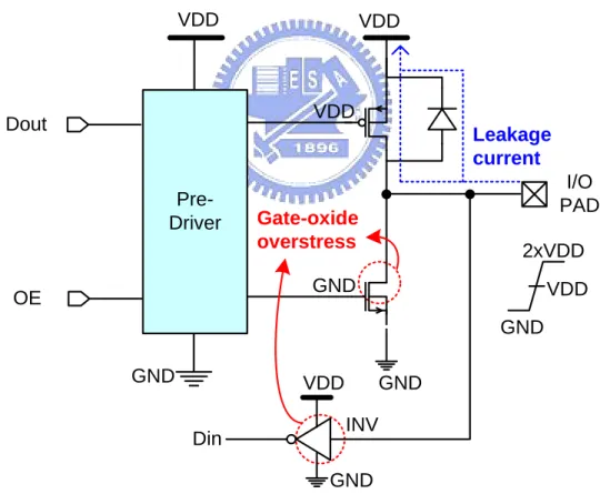
NTERFACEThe conventional tri-state I/O buffer with 1.2-V gate-oxide devices in a 0.13-µm CMOS process is shown in Fig. 2.2, where the power supply voltage (VDD) is 1.2 V. However, the input signal at the I/O pad in the mixed-voltage I/O interface may rise up to 2.5 V in the tri-state input (receive) mode. In the receive mode, the gate voltages of the pull-up PMOS device and the pull-down NMOS device in the I/O buffer are traditionally controlled at 1.2 V and 0 V to turn off the pull-up PMOS device and the pull-down NMOS device by the pre-driver circuit, respectively. When the input signal at the I/O pad raises up to 2.5 V in the tri-state input mode, the parasitic drain-to-well pn-junction diode in the pull-up PMOS device will be forward biased. Therefore, an undesired leakage current path flows from the I/O pad to the power supply voltage (VDD) through the parasitic pn-junction diode. Besides, because the gate voltage of the pull-up PMOS device is 1.2 V and the input signal at I/O pad is 2.5 V, the pull-up PMOS device will be turned on in such tri-state input mode to conduct another undesired leakage current path from the I/O pad to the power supply voltage (VDD). Such undesired leakage currents cause not only more power consumption in the electronic system but also malfunction in the whole electronic system.
Moreover, because the gate-drain voltage (Vgd) of the pull-down NMOS device and the gate-source voltage (Vgs) of the input buffer in Fig. 2.2 with 2.5-V input signal are higher than their voltage levels in the normal operation, such high voltage across the thin gate oxide of the pull-down NMOS device and the input buffer results in the gate-oxide overstress reliability issue [5], [15]. In addition, the pull-down NMOS device and the input buffer with a 2.5-V input signal may suffer serious hot-carrier degradation if their drain-source voltages are too high [13].
2.3 P
RIORM
IXED-V
OLTAGES
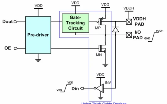
OLUTIONSThe design concept is shown in Fig. 2.3. To solve the problem of gate-oxide reliability, a CMOS technology with a dual-oxide option [16], [17] is used. Because the thick gate-oxide can avoid the instances of gate-oxide breakdown, transistors that may suffer excessive gate-oxide stress should be replaced with thick oxide devices, and other transistors remain unchanged. To solve the problem of undesired leakage paths by the pull-up PMOS and the parasitic drain-to-well pn-junction diode, a gate-tracking circuit and a higher external voltage (VDDH) are used.
In Fig. 2.3, the mixed-voltage I/O buffer transmits GND-to-VDD (low voltage level) output signals and receives GND-to-VDDH (high voltage level) input signals. The pre-driver circuit generates control signals to output transistors MN and MP. In the mixed-voltage I/O buffer, the output transistors, gate-tracking circuits, and input circuit, INV, are thick-oxide devices to overcome reliability problems. The pre-driver circuit uses thin-oxide devices since the input data come from internal core circuit with low voltage level. In order to avoid leakage current path from the I/O PAD to the power supply (VDD) through the parasitic drain-to-well pn-junction diode in the pull-up PMOS device, MP, a higher external voltage (VDDH) is used to bias the N-well of the MP. In addition, a gate-tracking circuit is required to avoid the leakage current path induced by the incorrect conduction of the MP. Such mixed-voltage interface applications with dual-oxide devices can successfully overcome the gate-oxide reliability and hot-carrier degradation problem.
Although the mixed-voltage I/O buffer with dual-oxide devices and an external N-well bias voltage can successfully solve these problems, there are some drawbacks in these mixed-voltage I/O buffers. Fist of all, an extra pad and another power supply (VDDH) are required for the external bias voltage, which results in the increase of
silicon area and cost. Second, the driving capacity is decreased due to higher threshold voltage of thick-oxide device when the gates of output transistors are controlled by pre-driver circuit with thin-oxide devices. Thirdly, the threshold voltage of the pull-up PMOS device (MP) is also increased since the N-well of the pull-up PMOS device (MP) is connected to a higher voltage (VDDH), which results in body effect. Because the driving capacity is decreased, the larger device dimension is required for the pull-up PMOS device to achieve the desired driving specifications. As a result, the silicon area in such I/O buffers is increased. Moreover, the manufacturing time of thick-oxide device is even three times large than that of thin-oxide device. For these reasons, the mixed-voltage I/O buffer with dual-oxide devices and an external n-well bias is unsuitable for the low-cost commercial ICs. Considering these limitations, several mixed-voltage I/O buffers with only thin-oxide devices have been reported in [18]-[21], [24]-[26].
Fig. 2.4 re-draws the mixed-voltage I/O buffer with stacked pull-up PMOS devices reported in [24]. Signal OE is the output-enable control signal. In the transmit mode, transistor MN1 is turned on and transistor MP2 is turned off, so that this I/O buffer drives the I/O pad according to the output signal Dout. In the tri-state input mode, transistor MN1 is turned off and transistor MP2 is turned on by the control signal OE at logic zero. If the input signal at the I/O pad is 5 V, the gate voltage of transistor MP1 and the floating n-well are pulled up to 5 V through transistor MP2 and the parasitic drain-to-well pn-junction diode in transistor MP0 to prevent the undesired leakage current paths from I/O pad to power supply voltage (VDD), respectively. Although this I/O buffer is simple, transistors MN0, MN1, and MP2 have the gate-oxide reliability problem in the tri-state input mode when the input signal has a 5-V voltage level. Besides, because the stacked PMOS devices with the floating n-well is applied to this I/O buffer, the PMOS devices in stacked
configuration occupy more silicon area.
Fig. 2.5 re-draws another mixed-voltage I/O buffer with stacked pull-up PMOS devices and stacked pull-down NMOS devices [25]. This I/O buffer uses transistors MP2, MN3, and MN4 as the gate-tracking circuit and transistors MP0, MP3, and MP4 as the dynamic n-well bias circuit. In the tri-state input mode with the control signal OE at GND, transistor MN4 is turned off and transistor MP2 is turned on. If the input signal at the I/O pad is 5 V, the gate voltage of transistor MP3 is biased at 5 V through transistors MP0 and MP2 to avoid the undesired leakage current path due to the incorrect conduction of transistor MP3. The floating n-well is biased at ~5 V through the parasitic drain-to-well pn-junction diode of transistor MP0. In the transmit mode with the OE control signal at VDD, transistor MN4 is turned on so that transistor MP3 is turned on, and transistor MP2 is kept off. Hence, this I/O buffer drives the I/O pad according to the output signal Dout. When the signal at the I/O pad is 0 V, the floating n-well is biased at 2.5 V through transistor MP4. When the input signal at the I/O pad is 2.5 V, the floating n-well is biased at ~2.5 V through the parasitic source-to-well pn-junction diodes of transistors MP3 and MP4. However, transistor MP2 has the gate-oxide reliability problem when the input signal at the I/O pad is 5 V in the tri-state mode. Besides, because the I/O buffer uses two PMOS devices, MP0 and MP3, in stacked configuration to drive the I/O pad, the stacked devices occupy more silicon area.
The mixed-voltage I/O buffer with a depletion PMOS device is re-drawn in Fig. 2.6 [18]. The depletion PMOS device MP2 in the I/O buffer is used as the gate-tracking circuit. In the tri-state mode, if the input signal at I/O pad is 5 V, the gate voltage of transistor MP0 is biased at 5 V through the depletion PMOS device MP2 to avoid the undesired leakage current path through the transistor MP0. This I/O buffer uses an extra pad that is connected to 5-V power supply (VDDH) to avoid the
undesired leakage current path through the parasitic drain-to-well pn-junction diode. However, using the depletion device increases mask layer and process modification. Thus, the fabrication cost of such I/O buffer design will be increased. In addition, using the extra n-well bias (VDDH) not only degrades the driving capacity of output device MP0 due to the body effect, but also increases the system cost.
Fig. 2.7 re-draws the mixed-voltage I/O buffer realized with only thin-oxide devices reported in [26]. In Fig. 2.7, the gate-tracking circuit and the dynamic n-well bias circuit are formed by transistors MP1, MP2, MP3, MP4, MN2, MN3, MN4, and MN5. In the transmit mode with signal OE at logic “1”, transistor MN4 is turned on to keep transistors MP3 and MP4 on. Thus, this I/O buffer drives the I/O pad according to signal Dout. Besides, because transistor MP3 is turned on, the floating n-well is biased at 2.5 V by transistor MP3 in the transmit mode. In the tri-state input mode with signal OE at logic “0”, transistor MN4 is kept off. If the input signal at the I/O pad is 5 V, the gate voltages of transistors MP0 and MP4 are biased at 5 V through transistor MP1 and MP2 to avoid the undesired leakage paths through the transistors MP0 and MP4. Besides, the floating n-well is also biased at ~5 V to avoid the undesired leakage path through the parasitic drain-to-well pn-junction diode of transistor MP0 when the voltage at the I/O pad is 5 V in tri-state input mode. When the input signal at the I/O pad is 0 V in the tri-state input mode, transistor MN3 is turned on to keep transistor MP3 on. So, the floating n-well is biased at 2.5 V.
Another mixed-voltage I/O buffer realized with only thin-oxide devices is re-drawn in Fig. 2.8 [19]. The gate-tracking circuit in Fig. 2.8 is composed of transistors MN3, MN4, MP2, MP3, and MP4. The dynamic n-well bias circuit in Fig. 2.8 is formed by transistors MN5, MP5, MP6, and MP7. Besides, the body terminals of all PMOS transistors in the gate-tracking circuit and the dynamic n-well bias circuit are connected to the floating n-well. Such I/O circuit shown in Fig. 2.8 can overcome
the gate-oxide reliability problem and avoid the undesired leakage paths. However, there are too many devices used to realize the desired functions of the gate-tracking circuit and the dynamic n-well bias circuit. More devices used in the mixed-voltage I/O cause more complex metal routing connection in the I/O cells.
2.4 A
M
IXED-V
OLTAGEI/O
B
UFFER WITHB
LOCKINGNMOS
ANDD
YNAMICG
ATE-C
ONTROLLEDC
IRCUITThe block diagram of mixed-voltage I/O buffer with a blocking NMOS and a dynamic gate-controlled circuit proposed in [14] is depicted in Fig. 2.9. Here, VDDH has a high voltage of 2xVDD, which can be generated by the on-chip charge pump circuit [22] or other high-voltage generators. Transistor MN1 is used to protect the conventional I/O buffer from the high-voltage overstress. The operations of the dynamic gate-controlled circuit in the proposed I/O buffer with blocking NMOS are listed in Table 2.1. When the I/O buffer is in the receive mode, the gate terminal (node 2) of MN1 is biased at VDD by the dynamic gate-controlled circuit, whereas the pull-up device MP0 and pull-down device MN0 are both turned off by the pre-driver. At this moment, if an input signal of logic ‘0’ (0V) is received from the I/O PAD, node 1 is discharged to 0 V through the transistor MN1, and this input signal can be successfully transferred to the node Din. When a logic ‘1’ (VDDH) signal is received at the I/O pad, the gate terminal of transistor MN1 is still biased at VDD, so the voltage on node 1 is pulled to “VDD−Vth”. A feedback device MP1 is added to restore
the voltage level on node 1 to VDD, which avoids the undesired static dc current through the inverter INV1. In this design, MN1, MP1, and inverter INV1 can convert the VDDH input signal to VDD signal successfully. Therefore, MN1 can protect the I/O buffer without suffering high-voltage overstress in both steady states of transmit
mode and receive mode.
Fig. 2.10 depicts the dynamic gate-controlled circuit of the I/O buffer in Fig 2.9, where MP2 and MP3 are designed with the cross-coupled structure. If the gate voltage of MP2 (or MP3) is pulled down, this transistor is turned on and pulls up the gate voltage of the other transistor to VDDH (2xVDD) to turn it off. For example, if the voltage on node 5 is lower than “VDDH−|Vtp|” and the voltage on node 6 is VDDH,
MN2 is turned on to keep the node 5 at VDD. Capacitors C1 and C2 are used to couple the signals from nodes 3 and 4 to nodes 5 and 6, respectively. The voltages across these capacitors are always VDD, because the voltage levels on the top plate and bottom plate of capacitors C1 and C2 are either VDD and 0V or 2xVDD and VDD. With these capacitors, when node 3 converts the voltage level from VDD to 0V, the voltage on node 5 is pulled down to VDD and then the voltage level on node 6 is pulled up to 2xVDD by transistor MP3. On the contrary, when the voltage level on node 4 is converted from VDD to 0V, the voltage on node 6 is pulled down to VDD, and that on node 5 is pulled up to 2xVDD by MP2. Initially, the voltages on nodes 3, 4, 5, and 6 could be unknown. If the voltages on nodes 5 and 6 are 2xVDD and VDD, and the voltages on nodes 3 and 4 are 0V and VDD, the voltages across capacitors C1 and C2 are 2xVDD and 0V, respectively, instead of both VDD. In order to overcome this problem, diode strings DS1 and DS2 are added. The turn-on voltages of the diode strings are designed to a little higher than VDD by using multiple diodes in stacked configuration. In order to prevent the leakage current path to the grounded p-type substrate, the diode-connected MOSFET or poly diode [23] is suggested. With these diode strings, if the voltage on node 3 is at 0V and that on node 4 is at VDD initially, the voltage on node 5 is clamped at the turn-on voltage (~VDD) of DS1. Therefore, MP3 is turned on to pull up the voltage on node 6 to 2xVDD. Thus, the voltages across capacitors C1 and C2 are both VDD.
In this mixed-voltage I/O buffer, the bulk of the blocking NMOS MN1 can be coupled to 0V (GND) without any gate-oxide reliability problem, even if the gate voltage of MN1 may be as high as VDDH (2xVDD). The reason is that this blocking NMOS MN1 is always turned on and the voltage across the gate oxide of MN1 is from the gate to the conducting channel, but not from the gate to its bulk. The gate oxides of all NMOS devices in the dynamic gate-controlled circuit are also safe because these NMOS devices are turned on when their gates are pulled up to VDDH.
Table 2.1
Operations of the dynamic gate-controlled circuit in the mixed-voltage I/O buffer with blocking NMOS [14]. Mode Transmitted Signals (Dout) Gate Voltage of MP0 (PU) Gate Voltage of MN1 (Node 2) Receive Mode X VDD VDD
Transmit Mode Low (0 V) VDD VDD Transmit Mode High (VDD) 0 V VDDH (2xVDD)
Fig. 2.1 Block diagram of bidirectional I/O buffer. . I/O PAD VDD Pre-Driver Dout VDD OE Din VDD GND INV GND GND Leakage current Gate-oxide overstress VDD GND VDD 2xVDD GND
Fig. 2.2 Conventional tri-state I/O buffer will suffer the circuit leakage and gate-oxide reliability issues in the mixed-voltage I/O interface.
Fig. 2.3 Block diagram of a mixed-voltage I/O buffer with dual-oxide devices and an external n-well bias voltage.
Fig. 2.5. Mixed-voltage I/O buffer with stacked pull-up PMOS devices and stacked pull-down NMOS devices [25].
Fig. 2.7. Mixed-voltage I/O buffer realized with only thin-oxide devices [26].
Fig. 2.9 The mixed-voltage I/O buffer with a blocking NMOS and a dynamic gate-controlled circuit.
Fig. 2.10 Circuit implementation of the dynamic gate-controlled circuit in the Fig. 2.9.
Chapter 3
1.2/2.5-V Mixed-Voltage I/O Buffer with
Gate-Tracking Circuit and Dynamic N-well Bias
Circuit by Only Using Thin Gate-Oxide Devices
3.1 I
NTRODUCTIONThere are a lot of drawbacks in the previous mixed-voltage I/O interface design with a dual-oxide option, like as extra voltage source and process cost. The prior designs of I/O interface are complicated and had been described in the chapter 2 already. In this chapter, a better mixed-voltage I/O interface is presented and proposed without extra process and voltage source in [21]. The presented design of mixed-voltage I/O interface buffer is simpler than the prior designs.
3.2 D
ESIGNC
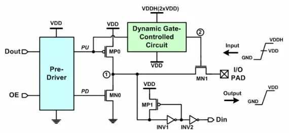
ONCEPTFig. 3.1 shows the presented mixed-voltage I/O buffer realized with a dynamic n-well bias circuit, and a gate-tracking circuit by only using thin gate-oxide devices [18]-[19], [24]-[26]. The stacked NMOS devices, MN0 and MN1, are used to avoid the high-voltage overstress on their gate oxide. The gate-tracking circuit shown in Fig. 3.1 is used to prevent the leakage current path which is resulted from the incorrect conduction of the pull-up PMOS device when the input signal is higher than VDD. As the mixed-voltage I/O buffer is operating in the transmit mode, the gate-tracking circuit must transmit the signal from the pre-driver circuit to the gate terminal of the
pull-up PMOS device, MP0, exactly. In the receive mode (tri-state input mode) with an input signal of 2xVDD, the gate-tracking circuit will charge the gate terminal of the MP0 to 2xVDD to completely turn off the MP0, and to avoid the leakage current from the I/O pad to the power supply (VDD). On the contrary, the gate-tracking circuit will keep the gate terminal of the MP0 at VDD to completely turn off the MP0, and to prevent the overstress on the gate oxide of the MP0 when the 0-V input signal is received from I/O PAD. Moreover, the dynamic n-well bias circuit shown in Fig. 3.1 is designed to prevent the leakage current path due to the parasitic drain-to-well pn-junction diode in the pull-up PMOS device MP0. In the transmit mode, the dynamic n-well bias circuit must keep the floating n-well bias at VDD so that the threshold voltage of the pull-up PMOS device isn’t increased due to the body effect. In the receive mode with an input signal of 2xVDD, the dynamic n-well bias circuit will charge the floating n-well to 2xVDD to prevent the leakage current from the I/O pad to the power supply (VDD) through the parasitic pn-junction diode. On the other hand, the dynamic n-well bias circuit will bias the floating n-well at VDD when the input signal at the I/O pad is 0V.
As shown in Fig. 3.1, the extra transistors, MN2 and MP1, which are compared to Fig. 2.3, are added in the input circuit. The transistor MN2 is used to limit the voltage level of input signal reaching to the gate oxide of inverter INV1. The transistor MP1 is used to prevent unnecessary leakage current in the inverter INV1. Because the gate terminal of transistor MN2 is connected to the power supply voltage (VDD), the input terminal of inverter INV1 will rise up to “VDD-Vth” when the input
signal at the I/O pad is 2xVDD in the receive mode. The transistor MP1 will pull the input node of inverter INV1 up to VDD when the output node of inverter INV1 is pulled down to 0V. Therefore, the gate-oxide reliability problem of the input buffer can be solved.
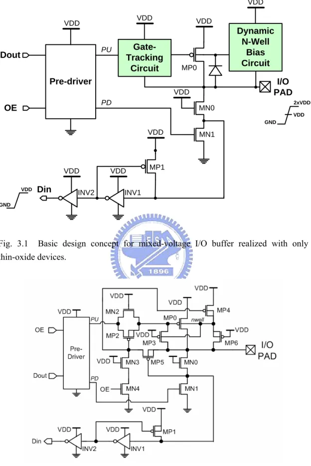
3.3 C
IRCUITD
ESCRIPTIONFig. 3.2 shows the mixed-voltage I/O buffer with the dynamic n-well bias circuit and gate-tracking circuit proposed in [21]. When the output control signal OE is at VDD (logic “1”), the mixed-voltage I/O buffer is operated in the transmit mode. The signal at the I/O pad follows the signal Dout, which is controlled by the internal circuits of IC. The pull-down signal, PD, produced by pre-driver is directly connected to the gate terminal of the pull-down NMOS device, MN1. The pull-up signal, PU, is connected to the gate terminal of the pull-up PMOS device, MP0, through the gate-tracking circuit which is composed of NMOS transistors MN2-MN4 and PMOS transistors MP2, MP3 and MP5. The transistors MN2 and MP2 comprise a transmission gate. The transistor MN3 in Fig. 3.2 is used to protect the transistor MN4 from gate-oxide reliability problem. The dynamic n-well bias circuit is composed of transistors MP4 and MP6. If the mixed-voltage I/O buffer is operating in transmit mode (OE = VDD), the gate terminal of MP4 will be biased at 0V to keep the floating n-well at VDD by turning on the transistor MP4. At this time, the PU signal is fully transmitted to the gate terminal of the pull-up PMOS device MP0 through the transmission gate, MN2 and MP2. As 0-V output signal is transmitted, the PD signal is set to VDD to turn on the transistor MN4. In the meanwhile, the PU signal is set to VDD to turn off the pull-up device MP0. Consequently, the voltage at the I/O pad and the gate voltage of transistor MP5 are discharged to 0 V through transistors MN0 and MN1. Transistor MP5 is turned on until the gate terminal of transistor MP2 is discharged to |Vtp| through transistors MN3 and MN4, where Vtp is the threshold
voltage of PMOS device.
When the proposed I/O buffer is operated in the receive mode, the PU and PD signals are kept at VDD and 0V, respectively, to turn off transistors MP0 and MN1.
Signal Din follows the signal at the I/O pad in the receive mode. In order to prevent the undesired leakage current from the I/O pad to the power supply (VDD) through the pull-up PMOS device MP0, transistor MP3 is used to track the signal at the I/O pad and to control the gate voltage of transistor MP0. When the voltage level at the I/O pad exceeds “VDD+|Vtp|,” such as 2xVDD, transistor MP3 is turned on to charge
the gate terminal of transistor MP0 up to 2xVDD. Thus, transistor MP0 is completely turned off to prevent the leakage current through its channel. If a 0-V input signal is received at I/O PAD, the floating n-well is biased at VDD through transistor MP4. As the mixed-voltage I/O is operating in the receive mode with an input signal of 2xVDD, another PMOS device MP6 is turned on to bias the floating n-well at 2xVDD. Also, transistor MP4 is turned off to prevent the leakage path by pulling up the gate terminal of MP4 to 2xVDD through transistor MP5. As a result, there is no leakage current path from the I/O pad to the power supply (VDD). Whenever the proposed mixed-voltage I/O buffer is in the transmit mode or the receive mode, the floating n-well is biased at VDD or 2xVDD directly. Thus, the subthreshold leakage problems do not occur in this proposed I/O buffer. Besides, transistor MP5 is also turned on to keep transistor MP2 off in order to prevent another leakage path from the gate terminal of transistor MP0 to the UP signal when the signal at the I/O pad is 2xVDD.
Transistors MN0 and MP1 with inverters INV1 and INV2 are used to transmit the input signal from the I/O pad to the internal node Din in the receive mode. Transistor MN0 is used to limit the voltage level of input signal reaching to the gate oxide of inverter INV1. The signal at the I/O pad can be successfully transmitted to the internal input node Din. This I/O buffer can be correctly operated with neither gate-oxide reliability problem nor any circuit leakage issue in the receive mode.
3.4 S
IMULATIONR
ESULTSIn this work, a completed I/O cell is constructed. The function block diagram is shown in Fig. 3.3 and the circuit schematic is shown in Fig. 3.4. This mixed-voltage I/O cell circuit includes input stage and output stage, pull-up resistor for floating I/O PAD, pre-driver circuit, gate-tracking circuit, floating n-well circuit and ESD protect device. The SPICE simulation waveforms of the mixed-voltage I/O cell with a 20-pF load at I/O pad are shown in Fig. 3.5 in UMC 0.13-μm 1.2-V CMOS process. Fig. 3.5(a) shows the behavior in transmit mode. The signal Dout with 0.5-ns rising and falling time is correctly transmitted to the I/O pad and the voltage level of floating N-well normally keeps at VDD. Fig. 3.5(b) shows that in receive mode (tristate mode). The signal Din correctly follows the signal with 0.5-ns rising and falling time at I/O pad and the voltage level of floating N-well is successfully pulled up to 2xVDD when the signal is 2xVDD at I/O pad. Fig. 3.5(c) shows the simulation waveform of the operation of the pull-up resistor, where the voltage level can be successfully pull up to weakly high when the pull-up resistor is turned on.
3.5 E
XPERIMENTALR
ESULTSFig. 3.6 is the die photo of the 1.2/2.5-V mixed-voltage I/O buffer with gate-tracking circuit and dynamic N-well bias circuit by only using thin gate-oxide devices. Fig. 3.7 shows the layout view of the 1.2/2.5-V mixed-voltage I/O buffer implemented in the UMC 130-nm 1.2-V CMOS process. The cell size of I/O cell is only 187μm×60μm (including the bond pad), which is the same as that of analog or power/ground cell in a standard I/O cell library.
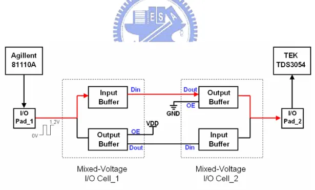
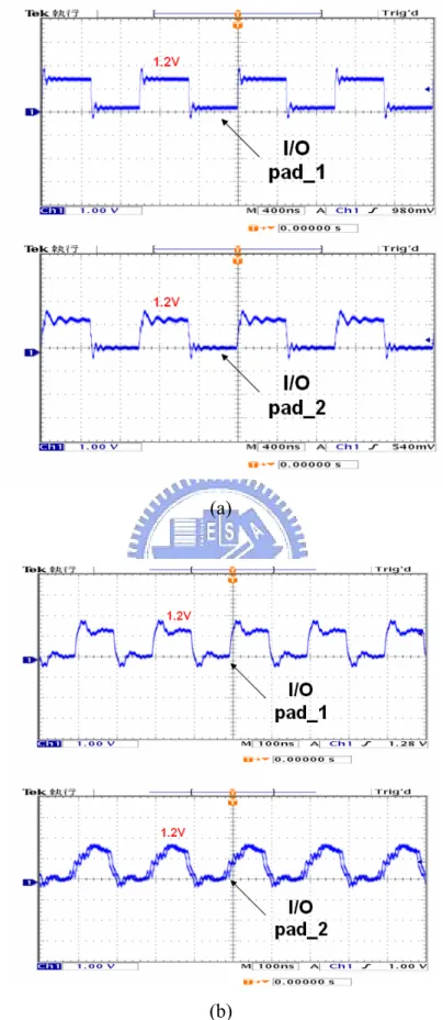
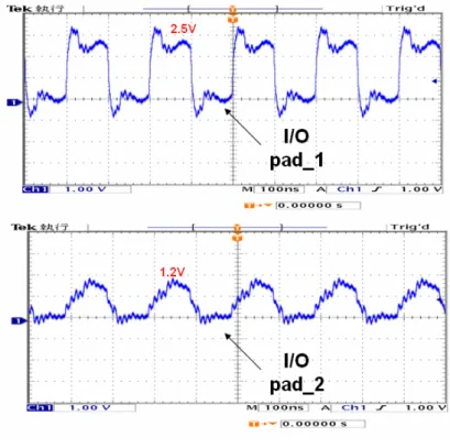
two proposed I/O cells are used and connected as the measurement setup in Fig. 3.8 for receiving 0/1.2-V signal of 1-MHz and 5-MHz. Here, the I/O cell_1 is used as the input cell to receive the external input signal from the pulse generator (81110A). The I/O cell_2 is used as the output cell to transmit the signal to the oscilloscope. As the measurement results shown in Fig. 3.9, the proposed I/O cell can successfully receive the 0/1.2-V input signal at the pad of the I/O Cell_1 and transmit to the pad of the I/O Cell_2.
To test the function of proposed I/O cell for receiving 0/2.5-V signal of 1-MHz and 5-MHz, two proposed I/O cells are used and connected as the measurement setup in Fig. 3.10. Here, the I/O cell_1 is used as the input cell to receive the external input signal from the pulse generator (81110A). The I/O cell_2 is used as the output cell to transmit the signal to the oscilloscope. As the measurement results shown in Fig. 3.11, the proposed I/O cell can successfully receive the 0/2.5-V input signal at the pad of the I/O Cell_1 and transmit to the pad of the I/O Cell_2 with the signal shifted in 0/1.2-V.
In Fig 3.12, the pull-up function is successfully verified with the voltage level at the pad pulled up to 0.92-V. From the measurement results, the 1.2/2.5-V mixed-voltage I/O buffer with gate-tracking circuit and dynamic N-well bias circuit by only using thin gate-oxide devices can be successfully operated in such a 1.2V/2.5V mixed-voltage I/O environment. The maximum operation frequency of the proposed I/O buffer depends on the output load and the device size of output circuit.
3.6 C
OMPARISONSTable 3.1 lists the features among these mixed-voltage I/O buffers. Since the new mixed-voltage I/O buffers and the prior I/O buffers reported in[19] and [24]-[26]
use the dynamic n-well biased technique, no extra pad and power supply is required. The new mixed-voltage I/O buffers in this work occupy smaller silicon area than the I/O buffers reported in [18]-[19], [24]-[25]. Although the circuit structures of the mixed-voltage I/O buffers reported in [24], [25] are simpler, these two I/O buffers have the gate-oxide reliability problem. In Fig. 2.4, transistors MN0, MN1, and MP2 have the gate-oxide reliability problem in the tri-state input mode when the input signal has a 5-V voltage level. In Fig. 2.5, transistor MP2 has the gate-oxide reliability problem when the input signal at the I/O pad is 5 V in the tri-state mode. In fig. 2.6, since the depletion PMOS is used to improve the gate-tracking circuit of the mixed-voltage I/O buffer reported in [18], extra mask and process modification are required to realize the depletion device. In fig. 2.4, fig. 2.5 and fig. 2.7 The prior mixed-voltage I/O buffers reported in [24]-[26] may have the subthreshold leakage problem, but the prior mixed-voltage I/O buffer reported in [19] and the new mixed-voltage I/O buffer don’t have. However, the new mixed-voltage I/O buffers occupy smaller silicon area than the prior I/O buffers [19], [24]-[26]. Thus, if the subthreshold leakage issue in the given CMOS process is serious, such as the 90-nm, 65-nm or more advanced CMOS process, the new mixed-voltage I/O buffer is recommended.
3.7 C
ONCLUSIONA new mixed-voltage I/O buffer with the stacked NMOS technique, dynamic n-well technique, and gate-tracking circuit have been successfully designed and implemented in UMC 0.13-μm 1.2-V CMOS process, which can be operated in the 1.2/2.5-V signal environment without the gate-oxide reliability problem. The new mixed-voltage I/O buffer can be applied for high-speed applications without the
gate-oxide reliability problem and the circuit leakage issue. The new mixed-voltage I/O buffer realized with 1xVDD devices can be easily applied in 1xVDD/2xVDD mixed-voltage interface.
Table 3.1
Comparison on features among the mixed-voltage I/O buffer designs.
Mixed-voltage I/O designs
N-well
bias Extra pad
Gate-oxide reliability issue Special device Subthreshold leakage issue Fig. 2.4 [24] Dynamic
bias No Yes No Yes
Fig. 2.5 [25] Dynamic
bias No Yes No Yes
Fig. 2.6 [18] Fixed bias Yes No Yes (Depletion PMOS) No Fig. 2.7 [26] Dynamic bias No No No Yes Fig. 2.8 [19] Dynamic bias No No No No Fig. 3.2 (This work) Dynamic bias No No No No
Pre-driver Dout VDD MP0 VDD I/O PAD Din OE Gate-Tracking Circuit VDD VDD MN0 MN1 Dynamic N-Well Bias Circuit VDD MP1 VDD GND VDD VDD INV1 VDD INV2 GND 2xVDD VDD PD PU
Fig. 3.1 Basic design concept for mixed-voltage I/O buffer realized with only thin-oxide devices.
Fig. 3.2 The mixed-voltage I/O buffer with gate-tracking circuit and dynamic n-well bias circuit proposed in [21].
Fig. 3.3 The function block of completed mixed-voltage I/O cell with gate-tracking circuit and dynamic n-well bias circuit.
Fig. 3.4 The circuit schematic of completed mixed-voltage I/O cell with gate-tracking circuit and dynamic n-well bias circuit.
Dout I/O PAD Floating N-Well (a) Dout I/O PAD Floating N-Well (b)
I/O PAD
(c)
Fig. 3.5 The simulated waveforms of the new proposed mixed-voltage I/O cell with a 20-pF load and 50-MHz I/O signal in (a) the transmit mode, (b) the tristate input (receive) mode, and (c) the transient simulation of pull-up for floating pad in 200-KHz.
Mixed-Voltage I/O Cells
Fig. 3.6 The die photo of the 1.2/2.5-V mixed-voltage I/O cells with gate-tracking circuit and dynamic N-well bias shown by only using only thin oxide devices.
Fig. 3.7 The layout view of the new 1.2/2.5-V mixed-voltage I/O cell with gate-tracking circuit and dynamic n-well bias.
Fig. 3.8 The measurement setup for testing the new 1.2/2.5-V mixed-voltage I/O cell with only thin oxide devices and dynamic n-well bias in transmit mode and receiving mode with 0/1.2-V input signal.
(a)
(b)
Fig. 3.9 The measurement results of the new 1.2/2.5-V mixed-voltage I/O cell in transmit mode and receiving mode with (a)1-MHz and (b)5-MHz 0/1.2-V input signal.
Fig. 3.10 The measurement setup for testing the new 1.2/2.5-V mixed-voltage I/O cell with gate-tracking circuit and dynamic n-well bias in transmit mode and receiving mode with 0/2.5-V input signal.
(a)
(b)
Fig. 3.11 The measurement results of the new 1.2/2.5-V mixed-voltage I/O cell in transmit mode and receiving mode with (a)1-MHz and (b)5-MHz 0/2.5-V input signal.
Fig. 3.12 The measurement result of the new 1.2/2.5-V mixed-voltage I/O cell for Pull-up function.
Chapter 4
New Proposed Mixed-Voltage Crystal Oscillator
Circuit I
4.1 I
NTRODUCTIONIn the advanced CMOS process technology, the complication and the requirement of precision have greatly increased in ICs, and also the clock rate is getting fast. In the same time, it becomes an important subject to sustain a high stability and precision of clock signal. And that is why a crystal oscillator is one of the most widely used circuits in modern digital ICs due to its stable and precise oscillation frequency.
A conventional crystal oscillator circuit is connected with a crystal between the output (XO) pad and the input (XI) pad for oscillation to generate the stable clock signal in the chip [27], [28]. In some applications, the clock signal will be directly provided from the external clock sources and sent into the chip through the input (XI) pad with the output (XO) pad floating. But, the conventional crystal oscillator circuit design with 1xVDD CMOS devices is unsuitable to receive the external clock signal with voltage level over 1xVDD, due to the gate-oxide reliability issue [5], [15] and the hot-carrier degradation issue [6].
The mixed-voltage I/O circuits had been discussed and presented in some prior papers [18]-[19], [24]-[26], but the mixed-voltage crystal oscillator circuit was never discussed before. In this chapter, a new mixed-voltage crystal oscillator circuit I realized with low-voltage CMOS devices is proposed without suffering the gate-oxide
reliability issue and undesired leakage current path. The new proposed mixed-voltage crystal oscillator circuit I has been designed and realized in UMC 130-nm 1.2-V CMOS process to server 1.2/2.5V mixed-voltage interface applications and TSMC 90-nm 1-V CMOS process to server 1/1.8V mixed-voltage interface applications.
4.1.1 Basic Resonance Theory
Fig. 4.1 shows a basic architecture of an oscillator circuit. This circuit includes two parts, an amplifier that provides a voltage gain A(s) and a feedback network β(s). When a trigger signal Ss is applied to the circuit, a total transfer function Af(s) of the loop can be got by
0 ( ) f S =β s S , SS +Sf =Si, S0 =A s S( ) i and hence 0 ( ) ( ) 1 ( ) ( f S S A s A s S A s β = = − s) 1 (4-1)
When the loop gain is
0 0 ( ) ( )= A jω β ωj (4-2) ( ) f A s = ∞ (4-3)
It means the signal with frequency ω0 could be held and amplified in the loop without
keeping the signal Ss. In order for an oscillator circuit to operate and by the condition of the equation (4-2), two conditions must be met: (A) The loop gain must be equal to unity; (B) The loop phase shift must be equal to 0, 2Pi, 4Pi, etc. radians. And these two conditions are called Barkhausen criterion.
4.1.2 Equivalent Circuit of Crystal
Quartz crystal units serve as the controlling element of oscillator circuits by conversion of mechanical vibrations to electrical current at a specific frequency. This is accomplished by means of the "Piezoelectric" effect. Piezoelectricity is electricity created by pressure. In a piezoelectric material, the application of mechanical pressure along an axis will result in the creation of an electrical charge along an axis at right angles to the first. In some materials, the obverse piezoelectric effect is found, which means that the imposition of an electric field on the ends of an axis will result in a mechanical deflection along an axis at right angles to the first. Quartz is uniquely suited, in terms of mechanical, electrical and chemical properties, for the manufacture of frequency control devices. Quartz crystal units which oscillate within certain frequency and temperature ranges have been developed over the years.
The equivalent circuit of a crystal is shown in Fig. 4.2. Rs is the effective series
resistance in the crystal; as well as Ls and Cs are the motional inductance and
capacitance of the crystal. Cp is the parasitic shunt capacitance due to the electrodes.
In parallel resonant mode, the crystal will look inductive to the circuit. At the resonant frequency, the crystal will look and perform like a low resistance. And some typical crystal parameters in different oscillation frequency are listed in Table 4.1.
Fig. 4.3 shows the reactance-frequency plot of the crystal. And the equivalent circuit impedance is given by the equation (4-4)
2 2 1 ( ) s s s s p p s C L Z j L C C C C ω ω ω − = ⎡ ⎤ − ⎣ − + ⎦ (4-4)
When the crystal is operating at series resonance, it looks purely resistive and the series resonance frequency (fs) is given by the equation (4-5)
1 2 s s s f L C π = (4-5)
When the crystal is operating in parallel resonant mode, it looks inductive. In this mode, the frequency (fa) of oscillation is given by the equation (4-6)
1 2 a S P S S P f C C L C C π = + (4-6)
4.1.3 Pierce-Type Crystal Oscillator
The conventional Pierce-type crystal oscillator circuit is shown in Fig. 4.4. This circuit consists of two parts. One is an inverting amplifier that supplies a voltage gain and 180 degree phase shift, which is integrated into the chip with the XI and XO pads. The other is a frequency selective feedback network, which is out of the chip. The crystal combined with C1 and C2 to form a feedback network that tends to stabilize the
frequency and supply 180 degree phase shift to the feedback path. The feedback resistance, Rf, is used to bias the inverting amplifier around half of power supply
voltage, therefore the inverting amplifier is operating in the high gain linear region. In steady state, this circuit has an overall phase shift around 360 degree. This satisfies one of the conditions required to sustain oscillation. The other condition for proper start-up and sustaining oscillation is that the closed loop gain should be over or equal to unity.
4.1.4 Evaluation of Minimum Inverting Gain gm
equivalent circuit diagram, in which the crystal is replaced by Ls, Cs, Rs and Cp. The
inverter is replaced by its output impedance Ro and the output current from the transconductance gain: Iout= gm*V1. Rf is a feedback resistance to force the gate input
to its threshold level to provide starting up. In most microcontroller-types the feedback transistor Rf is already integrated as a semiconductor resistor parallel to the
inverting gate.
A very convenient way and also rather easy to prove the oscillation condition is to transfer all these elements in series with Rs by means of the power dissipation rule,
saying that the elements Ro, Rf and gm*V1 are replaceable by a resistor in series with
Rs, if this gives the same dissipation or damping to the circuit. Then the oscillation
condition is true, if the total value of the resistive elements, including the own damping Rs of the crystal is less than zero.
After transferring all resistive elements into the series branch, the simplified resonance calculation model of fig. 4.6 can be used. In this figure, Co is the total
parallel capacitance, including load capacitance Cload formed by the capacitances C1
and C2 in series and the parasitic capacitance Cpar at input and output parallel with the
gate and Cp as following:
1 2/( 1 2) o p load par load C C C C C C C C C = + + = +
The value of Rt is given by Rt= Rs + Rf
’
+Ro’
+Rgm’
. Assuming that in resonance, IRt= ICo, then it follows for Rf’:
' 2 2 0 0 2 2 0 0 ( ) / ' ( ) / ( ) f f t t o R R X f R f R C X X f X P P V R I R I I V C V R V C R ω ω = = ∗ = = = ∗ f '
2 0 0 1 ' ( ) f f R C R ω = ∗ (4-7)
For the output impedance Ro follows with PRo = PRo’:
' 2 2 2 2 1 1 2 0 0 2 2 1 1 2 0 0 ( ) / ' /( ) ( /( )) / ( ) Ro Ro o Ro o X Ro Co X X o X P P V R I R V V C C C I I V C V C C C R V C R ω ω = = ∗ = ∗ + = = ∗ + = ∗ o' 2 1 2 2 0 0 1 2 1 ' ( ) ( ) o o C R C R C C ω = ∗ ∗ + (4-8)
Transferring Iout= gm*V1 to Rgm
’
means, with P (gm*V1) = PRgm’
:1 ( ) ' 2 1 2 1 2 1 2 2 1 1 2 2 2 1 2 1 2 0 0 ' /( ) /( ) /( ) ( ) ' gm V R gm Rt gm X X Rt Co X X P P gmV V I R V V C C C V V C C C I I gm V C C C C V ω C R ⋅ = − = ∗ = ∗ + = ∗ + = − ⋅ ⋅ ⋅ + = 2 gm 1 2 2 2 0 0 1 2 ' ( ) ( ) gm C C gm R C C C ω − = ∗ + (4-9)
Combining these equations, we obtain for the total series resistance:
2 1 1 2 2 0 0 0 1 2 1 2 1 1 1 ( ) ( ) ( ) t s m f C C C R R g C R R C C C C ω ⎧ ⎫ ⎪ ⎪ = + ⎨ + − ⎬ + + ⎪ ⎪ ⎩ ⎭ 2 (4-10)
The circuit will oscillate, if the value of Rt is zero or negative. So the minimum value
of gm should be: 2 2 2 0 0 1 2 1 2 1 2 1 2 2 ( ) ( ) 1 ( ) 1 m s f o C C C C C C g R C C R C C R C ω + + ≥ × + + 1 (4-11)
To achieve minimum requirement of oscillation, both load capacitances should be equal. In this case we find:
2 0 0 4 1 .min 4( ) m s f o g R C R R ω ≥ × + + (4-12)
4.2 G
ATE-O
XIDER
ELIABILITYI
SSUE INC
ONVENTIONALC
RYSTALO
SCILLATORC
IRCUITIn the advanced CMOS process, the devices with thinner gate oxide can be operated at a higher operating speed under a lower VDD supply voltage. The power supply voltage level has been decreased from 2.5V to around 1V to maintain the gate-oxide reliability and to overcome the hot-carrier degradation. However, many other components on the board or in the system are still operated at another higher voltage level such as 3.3V or 5V. This is also a challenge to the interface circuit to avoid the gate-oxide reliability problem.
Fig. 4.7 shows the conventional crystal oscillator circuit realized with the 1×VDD devices. When this circuit was used in the mixed-voltage interface, it will suffer the gate-oxide reliability issues. When the EN signal is kept at VDD and the external input clock signal at the XI pad rises up to 2×VDD. The pull-up PMOS and pull-down NMOS will suffer the gate-oxide overstress issue. In order to avoid the gate-oxide reliability issue, the devices which suffer the gate-oxide overstress could be replaced by the thick-oxide devices. However, with both of the thick-oxide and thin-oxide devices in a chip, the fabrication cost of CMOS process is increased.
![Fig. 2.5. Mixed-voltage I/O buffer with stacked pull-up PMOS devices and stacked pull-down NMOS devices [25]](https://thumb-ap.123doks.com/thumbv2/9libinfo/8611438.190758/29.892.189.704.119.502/mixed-voltage-buffer-stacked-pmos-devices-stacked-devices.webp)
![Fig. 2.7. Mixed-voltage I/O buffer realized with only thin-oxide devices [26].](https://thumb-ap.123doks.com/thumbv2/9libinfo/8611438.190758/30.892.170.724.124.550/fig-mixed-voltage-i-buffer-realized-oxide-devices.webp)