銅閘極搭配氮化鉿擴散阻擋層之金氧半電容研究
87
0
0
全文
(2) 銅閘極搭配氮化鉿擴散阻擋層之金氧半電容研究 A Study on MOSCAPs with Cu Gate Electrode and HfN Diffusion Barriers 研 究 生:王 凱 立. Student:Kai-Li Wang. 指導教授:張 俊 彥 博士. Advisor:Dr. Chun-Yen Chang. 國 立 交 通 大 學 電子工程學系. 電子研究所碩士班. 碩 士 論 文. A Thesis Submitted to Institute of Electronics College of Electrical Engineering and Computer Science National Chiao Tung University for the Degree of Master of Science in Electronics Engineering June 2004 Hsinchu, Taiwan, Republic of China. 中 華 民 國 九 十 三 年 六 月.
(3) 銅閘極搭配氮化鉿擴散阻擋層之 金氧半電容研究 研究生:王凱立. 指導教授:張俊彥 博士. 國 立 交 通 大 學. 電子工程學系. 電子研究所碩士班. 摘 要 隨著元件線寬的縮小,用傳統的複晶矽閘極所製作出來的元件特 性已不能滿足對於元件品質的要求。有許多的研究指出利用金屬閘極 來取代複晶矽閘極可以避免掉許多問題。所以使用金屬閘極已經成為 了在元件線寬縮小過程之中的一種趨勢。銅有著電阻係數低的特性, 所以可以利用來當作閘極的金屬材料。但是銅在半導體製程中會造成 嚴重的污染問題,因此我們需要一個阻擋層來阻止銅離子擴散到介電 材料跟矽基板。而氮化鉿的熱穩定性佳且結構緻密,如果應用在做為 銅的擴散阻擋層,將會是個非常適合的擴散阻擋層材料。. i.
(4) 在本實驗中,我們利用銅來當作閘極的材料並搭配上氮化鉿來作 為阻擋層。在電性跟可靠度的量測資料中可以看出,當氮化鉿的厚度 超過 25 奈米的時候,在電性跟可靠度上的表現幾乎是相差無幾的。但 是當氮化鉿的厚度降至 20 奈米時,可靠度上的表現就變差了一些。從 二次離子質譜儀的分析資料中我們可以得知,造成可靠度下降的主要 因素在於銅離子擴散到介電材料之中而影響到電容的特性。在這同 時,我們也比較了擁有 28 奈米氮化鉿或 34 奈米氮化鉭阻擋層的銅閘 極電容的可靠度。我們發現擁有 28 奈米氮化鉿阻擋層的銅閘極電容的 可靠度表現會比擁有 34 奈米氮化鉭阻擋層的銅閘極電容要好。接著我 們也發現了對於使用銅閘極和 28 奈米氮化鉿阻擋層的電容結構來 說,攝氏四百度、氮氣環境下三十分鐘的爐管退火是個很適合的熱退 火條件。在這個條件下可以移除掉部分製程中所產生的氧化層電子與 缺陷,而且不會降低電容的可靠度。但是當熱退火溫度超過五百度時, 電容的可靠度就會受到影響,所以不適合用在這個結構的製程。 . ii.
(5) A Study on MOSCAPs with Cu Gate Electrode and HfN Diffusion Barriers. Student:Kai-Li Wang. Advisor:Dr. Chun-Yen Chang. Department of Electronics Engineering and Institute of Electronics National Chiao Tung University, Hsinchu, Taiwan. Abstract Accompany with the scaling down of the devices, the conventional polysilicon gate can not satisfy the performance requirements of the integrate circuits. Many researches indicated that using metal gate to replace the polysilicon gate can eliminate many issues, such as the poly depletion, boron penetration, and the RC delay. Using metal to be the gate electrode is the trend to promote the performance of MOSFETs when the devices scaling down. Copper has lower resistivity and suits to be the gate electrode. But copper has serious contamination problems for device applications. Thus we need a diffusion barrier to block copper ions diffusion into the dielectrics and the silicon substrate. In respect of the thermal stability and high density, HfN is a candidate material to be the diffusion barrier.. iii.
(6) In our experiments, we use the copper as the gate electrode and the HfN as the diffusion barrier of copper. We can find the electrical properties and reliability are almost identical when the thickness of HfN is over 25 nm, and degraded when the thickness of HfN is down to 20 nm. According to the SIMS analysis data, we found the copper ions diffusion into the dielectric is the main reason why the electrical properties and reliability were degraded. It also proves the HfN layer can block the diffusion of copper ions. We also compare the reliability of copper gate MOSCAPs with 28-nm-thick HfN and 34-nm-thick TaN diffusion barriers. The copper gate MOSCAPs with 28-nm-thick HfN diffusion barrier shows better reliability than that with 34-nm-thick TaN diffusion barrier sample. Afterwards, we found the 400°C furnace annealing in N2 ambient for 30 minutes is a suitable condition for the copper gate MOSCAPs with HfN diffusion barrier. The 400°C annealing can remove the plasma induced oxide charge and did not degrade the reliability of copper gate MOSCAPs with 28-nm-thick HfN diffusion barrier. When the annealing temperature was increased over 500°C, the copper ions will diffusion into the dielectrics and the reliability will be degraded.. iv.
(7) 誌 謝. 在兩年的碩士班生活裡,學習到了許多的課業上、實驗上以及人 生上的知識。也因為有著許多人的幫助,我才能順利的完成碩士班的 學業。首先要感謝的是我的指導教授張俊彥校長,在繁忙的校務工作 下仍撥冗給予指導及鼓勵,老師的遠見及胸懷更是我們該學習的目 標。再來要感謝的是國家奈米實驗室的簡昭欣博士,簡博士在實驗及 論文上的指導給我很大啟發,也讓我能更瞭解實驗中問題關鍵的所在 及其背後的意涵。 我還要特別感謝彭辭修學長及陳經緯學長在課業上、實驗上、量 測上及論文上的照顧及幫助。如果沒有他們的指導及幫忙,這本碩士 論文可能會沒辦法順利的寫出。尤其是彭辭修學長,幫我訂正論文中 的錯誤,真是辛苦了。也感謝而國家奈米實驗室的楊明瑞學長、呂正 傑學長、黃英傑學長在實驗上的幫忙。還有我的同學及室友們:怡誠、 嘉欣、慶宗、心卉、國誠、柏青、信宏、盈彰。在實驗上及生活上你 們都幫了我非常大的忙,真的是非常的感謝你們。 最後我要感謝我的家人在這兩年裡一直在背後給予無限的支持及 鼓勵,讓我能夠專心於碩士班的學業,不用擔心生活上的瑣事,讓我 能夠順利的完成學業,非常的謝謝你們。. v.
(8) Contents. Abstract (Chinese) ......................................................................................................... i Abstract (English) ........................................................................................................ iii Acknowledgments .......................................................................................................... v Contents ......................................................................................................................... vi Table Captions .............................................................................................................. ix Figure Captions ............................................................................................................. x. Chapter 1 Introduction ........................................................................................ 1 1.1 General Background ....................................................................................... 1 1.2 The Choice of Cu Diffusion Barrier .............................................................. 5 1.3 Motivation ........................................................................................................ 7 1.4 Organization of the Thesis .............................................................................. 8. Chapter 2 Experimental Procedure .............................................................. 10 2.1 Standard Process ........................................................................................... 10 2.2 Thermal Treatments ...................................................................................... 11 2.3 Measurements ................................................................................................ 11. vi.
(9) 2.3.1 Electrical Measurements ...................................................................... 11 2.3.2 Time Dependent Dielectric Breakdown (TDDB), Lifetime & Charge to Breakdown (QBD) Measurements ...................................... 11 2.3.3 Bias Temperature Stress (BTS) Measurements .................................. 12 2.3.4 Elevated Temperature Measurements ................................................ 12 2.3.5 Material Analysis .................................................................................. 13. Chapter 3 Electrical Characteristics and Reliability of Copper Gate MOSCAPs with HfN Diffusion Barrier ....................... 14 3.1 Electrical Characteristics of Cu Gate MOSCAPs with Different Thickness of HfN ........................................................................................... 14 3.2 Reliability of Cu Gate MOSCAPs with Different Thickness of HfN ........ 15 3.3 Comparison of HfN and TaN Diffusion Barrier ......................................... 18 3.4 Summary ........................................................................................................ 19. Chapter 4 Thermal Stability of Copper Gate MOSCAPs with HfN Diffusion Barrier ....................................................... 21 4.1 Electrical Characteristics of Annealed Cu/HfN/SiO2/p-Si ........................ 21 4.2 Conduction Mechanism of Annealed Cu/HfN/SiO2/p-Si ........................... 24. vii.
(10) 4.3 Bias Temperature Stress ............................................................................... 26 4.4 Reliability ....................................................................................................... 28 4.5 Summary ........................................................................................................ 30. Chapter 5 Conclusion ......................................................................................... 32 Vita. viii.
(11) Table Captions. Table 1-1 The resistivity of various barrier layers. Table 4-1 Comparison of barrier height, work function, flat band, and charge concentration under gate injection for the as deposited, 400ºC, 500ºC, and 600ºC annealed Cu/HfN/SiO2/p-Si MOSCAPs with 28-nm-thick HfN diffusion barrier.. ix.
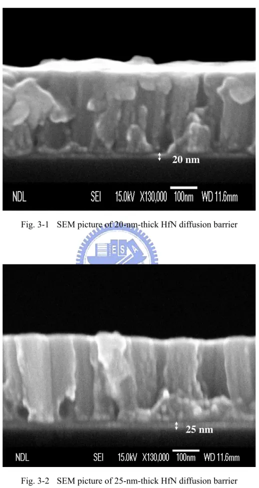
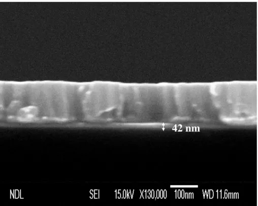
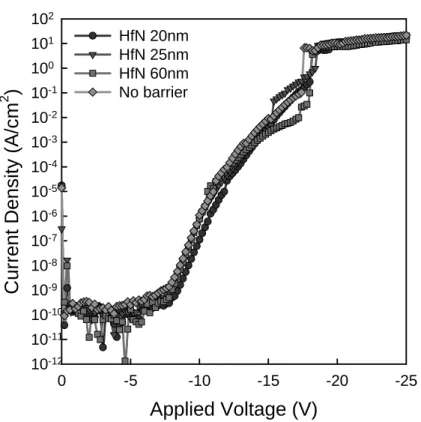
(12) Figure Captions. Chapter 1 Fig. 1-1 The Barrier layer X is between material A and B. Fig. 1-2 (a) sacrificial barrier (b) stuffed barrier (c) passive compound barrier (d) amorphous barrier.. Chapter 2 Fig. 2-1 Key process of fabrication Cu/HfN/SiO2/p-Si MOSCAP and the cross section structure of the capacitor. Fig. 2-2 Dielectric breakdown was defined at the point which current density increase more than three orders. Chapter 3 Fig. 3-1 SEM picture of 20-nm-thick HfN diffusion barrier. Fig. 3-2 SEM picture of 25-nm-thick HfN diffusion barrier. Fig. 3-3 SEM picture of 42-nm-thick HfN diffusion barrier. Fig. 3-4 SEM picture of 60-nm-thick HfN diffusion barrier. Fig. 3-5 C-V curves for the Cu gate MOSCAPs with 20-nm-thick, 25-nm-thick, 42nm-thick, and 60-nm-thick HfN diffusion barrier and no barrier sample. Fig. 3-6 I-V curves for the Cu gate MOSCAPs with 20-nm-thick, 25-nm-thick, 42-. x.
(13) nm-thick, and 60-nm-thick HfN diffusion barrier and no barrier sample. Fig. 3-7 Weibull plot of effective breakdown field for the Cu gate MOSCAP with 20nm-thick, 25-nm-thick, and 60-nm-thick HfN diffusion barrier and no barrier sample. Fig. 3-8 Weibull plot of charge to breakdown for the Cu gate MOSCAPs with 20nm-thick, 25-nm-thick, 42-nm-thick, and 60-nm-thick HfN diffusion barrier and no barrier sample. Fig. 3-9 The Weibull plot of TDDB at 13.06 MV/cm for the Cu gate MOSCAPs with 20-nm-thick to 60-nm-thick HfN diffusion barrier and no barrier control samples. Fig. 3-10 The Weibull plot of TDDB at 12.82 MV/cm for the Cu gate MOSCAPs with 20-nm-thick and 28-nm-thick HfN diffusion barrier. Fig. 3-11 Lifetime of the Cu gate MOSCAPs with 20-nm-thick and 28-nm-thick HfN diffusion barrier. Fig. 3-12 SIMS analysis of the Cu gate MOSCAPs without diffusion barrier. Fig. 3-13 SIMS analysis of the Cu gate MOSCAPs with 20-nm-thick HfN diffusion barrier. Fig. 3-14 SIMS analysis of the Cu gate MOSCAPs with 25-nm-thick HfN diffusion barrier.. xi.
(14) Fig. 3-15 SIMS analysis of the Cu gate MOSCAPs with 60-nm-thick HfN diffusion barrier. Fig. 3-16 SEM picture of 28-nm-thick HfN diffusion barrier. Fig. 3-17 SEM picture of 34-nm-thick TaN diffusion barrier. Fig. 3-18 The C-V curves for Cu gate MOSCAPs with 28-nm-thick HfN and 34-nmthick TaN diffusion barrier. Fig. 3-19 The I-V curves for Cu gate MOSCAPs with 28-nm-thick HfN and 34-nmthick TaN diffusion barrier. Fig. 3-20 The charge to breakdown for Cu gate MOSCAPs with 28-nm-thick HfN and 34-nm-thick TaN diffusion barrier. Fig. 3-21 TDDB of the Cu gate MOSCAPs with 28-nm-thick HfN and 34-nm-thick TaN diffusion barrier. Fig. 3-22 Lifetime of the Cu gate MOSCAPs with 28-nm-thick HfN and 34-nm-thick TaN diffusion barrier.. Chapter 4 Fig. 4-1 Sheet resistance for the as deposited, 400°C, 500°C, and 600°C annealed Cu/HfN/SiO2 /p-Si MOSCAPs with 28-nm-thick HfN diffusion barrier. Fig. 4-2 C-V curves of 100 KHz for the as deposited, 400°C, 500°C, and 600°C annealed Cu/HfN/SiO2/p-Si MOSCAPs with 28-nm-thick HfN diffusion. xii.
(15) barrier. Fig. 4-3 C-V curves of different frequencies for the as deposited Cu/HfN/SiO2/p-Si MOSCAPs with 28-nm-thick HfN diffusion barrier. Fig.4-4. C-V curves of different frequencies for Cu/HfN/SiO2/p-Si MOSCAPs with 28-nm-thick HfN diffusion barrier after 400°C annealing.. Fig.4-5. C-V curves of different frequencies for Cu/HfN/SiO2/p-Si MOSCAPs with 28-nm-thick HfN diffusion barrier after 500°C annealing.. Fig.4-6. C-V curves of different frequencies for Cu/HfN/SiO2/p-Si MOSCAPs with 28-nm-thick HfN diffusion barrier after 600°C annealing.. Fig.4-7. Hysteresis of C-V curves for the as deposited Cu/HfN/SiO2/p-Si MOSCAPs with 28-nm-thick HfN diffusion barrier.. Fig.4-8. Hysteresis of C-V curves for Cu/HfN/SiO2/p-Si MOSCAPs with 28-nm-thick HfN diffusion barrier after 400°C annealing.. Fig.4-9. Hysteresis of C-V curves for Cu/HfN/SiO2 /p-Si MOSCAPs with 28-nm-thick HfN diffusion barrier for 500°C annealing.. Fig.4-10 Hysteresis of C-V curves for Cu/HfN/SiO2/p-Si MOSCAPs with 28-nm-thick HfN diffusion barrier after 600°C annealing. Fig.4-11 I-V curves for the as deposited, 400°C, 500°C, and 600°C annealed Cu/HfN/SiO2/p-Si MOSCAPs with 28-nm-thick HfN diffusion barrier.. xiii.
(16) Fig.4-12 Weibull plot of effective breakdown electric field for Cu/HfN/SiO2/p-Si MOSCAPs with 28-nm-thick HfN diffusion barrier after 400°C, 500°C, and 600°C annealing. Fig.4-13 Conduction mechanism fitting under gate injection for the as deposited Cu/HfN/SiO2/p-Si MOSCAPs with 28-nm-thick HfN diffusion barrier. Fig.4-14 Conduction mechanism fitting under gate injection for the Cu/HfN/SiO2/p-Si MOSCAPs with 28-nm-thick HfN diffusion barrier after 400°C annealing. Fig.4-15 Conduction mechanism fitting under gate injection for the Cu/HfN/SiO2/p-Si MOSCAPs with 28-nm-thick HfN diffusion barrier after 500°C annealing. Fig.4-16 Conduction mechanism fitting under gate injection for the Cu/HfN/SiO2/p-Si MOSCAPs with 28-nm-thick HfN diffusion barrier after 600oC annealing. Fig.4-17 Barrier height under gate injection for the as deposited, 400°C, 500°C, and 600°C annealed Cu/HfN/SiO2/p-Si MOSCAPs with 28-nm-thick HfN diffusion barrier. Fig.4-18 (a) Band diagram under gate injection for as deposited Cu/HfN/SiO2/p-Si MOSCAPs with 28-nm-thick HfN diffusion barrier. Fig.4-18 (b) Band diagram under gate injection for Cu/HfN/SiO2/p-Si MOSCAPs with 28-nm-thick HfN diffusion barrier after 400°C annealing. Fig.4-19 C-V curves before and after 1000 sec BTS at 50°C, 100°C, and 150°C for. xiv.
(17) Cu/HfN/SiO2/p-Si MOSCAPs with 28-nm-thick HfN diffusion barrier after 400°C annealing. The field applied was +1 MV/cm. Fig.4-20 C-V curves before and after 1000 sec BTS at 50°C, 100°C, and 150°C for Cu/HfN/SiO2/p-Si MOSCAPs with 28-nm-thick HfN diffusion barrier after 500°C annealing. The field applied was +1 MV/cm. Fig.4-21 C-V curves before and after 1000 sec BTS at 50°C, 100°C, and 150°C for Cu/HfN/SiO2/p-Si MOSCAPs with 28-nm-thick HfN diffusion barrier after 600°C annealing. The field applied was +1 MV/cm. Fig.4-22 Flat band shift before and after 1000 sec BTS at 50°C, 100°C, and 150°C for Cu/HfN/SiO2/p-Si MOSCAPs with 28-nm-thick HfN diffusion barrier after 400°C, 500°C, and 600°C annealing. The field applied was +1 MV/cm. Fig.4-23 Charge to breakdown of as deposited, 400°C, 500°C, and 600°C annealed Cu/HfN/SiO2/p-Si MOSCAPs with 28-nm-thick HfN diffusion barrier. Fig.4-24 TDDB of as deposited, 400°C, 500°C, and 600°C annealed Cu/HfN/SiO2 /p-Si MOSCAPs with 28-nm-thick HfN diffusion barrier. Fig.4-25 Lifetime of as deposited, 400°C, 500°C, and 600°C annealed Cu/HfN/SiO2 /p-Si MOSCAPs with 28-nm-thick HfN diffusion barrier.. xv.
(18) Chapter 1. Introduction. 1.1 General background In recent years, dimension scaling down of integrated circuits is necessary in order to achieve better performance in silicon-based devices. Gate engineering is one of the most important issues of integrated circuits during scaling down [1]-[3]. There are some problems using polysilicon as the gate material, such as poly depletion, high resistance, and boron penetration into the channel region in submicron CMOS technology node [4]. Polysilicon gate depletion increases the equivalent gate dielectric thickness by about 0.3 nm and degrades channel current drive capability [5], [6]. High gate resistance increases the RC delay and degrades the performance of the devices in high frequency [7]. Although using salicide can release the high gate resistance problem, it is difficult for salicide to maintain a proper aspect ratio of gate stacks whiles the devices continuously scaling down [8]. Boron penetration in p-channel metal oxide semiconductor field effect transistors (p-MOSFETs) reduces the gate oxide reliability and the control ability of threshold voltage [9]. On the other hand, metal gate has been investigated to replace the polysilicon gate to solve the problems we mentioned above. To choose a suitable material to be the metal gate, several issues should be considered. 1.
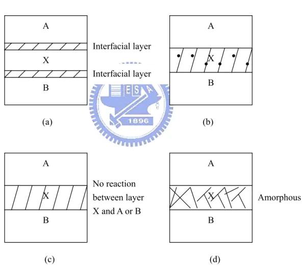
(19) to satisfy the manufacturability and performance. High temperature processes must be kept off, because high temperature processes will cause the instability of the metal film. Thus, low temperature or low thermal budget processes must be developed. The requirements of metal gate are low resistivity, suitable work function, high thermal dynamic stability, and good chemical durability under wet chemical processing [10]. The resistivity of copper (1.67 µΩ-cm) is smaller than aluminum (2.66 µΩ-cm) which is the most often used metal in conventional IC fabrication. And the resistance electromigration of copper (0.97 eV) is larger than aluminum (0.62 eV) [11]. Because of the low resistivity, copper is a potential material as the gate metal. Nevertheless, there are still some problems with copper in ultra-large-scale integration (ULSI) circuits. The problems are high diffusivity, susceptibility to oxidation and corrosion, high chemical reactivity, and hard to be dry etched in process [12]. By the reasons we mentioned above, the diffusion barrier is significant to the reliability of integrated circuits with copper metallization. Before the selection of the material of diffusion barrier, the knowledge of what kind of the properties are diffusion barrier needed should be learned. Below is the list of the notion of diffusion barriers [13], [14]:. (1) If the barrier layer X is between materials A and B (Fig. 1-1), the barrier should be thermal dynamically stable when in contact with both A and B.. 2.
(20) (2) X should prevent harmful interdiffusion between A and B. Thus, diffusivity of both materials A and B in barrier layer should be as low as possible. It means that the X becoming a kinetic barrier to A and B. The most preferred structure would be single-crystalline, but this solution lies generally beyond the capabilities of current technology. A practical second choice is the amorphous structure. However, the amorphous structure is negation with the requirement for the thermodynamic stability. (3) The barrier layer should form low resistance contacts with materials A and B and be at least a reasonable thermal conductor. The resistivity of the barrier layer itself is usually smaller than 2500 µΩ-cm because of its small thickness compared to that of material A and B. (4) X should have excellent adhesion to all materials which can be used in the metallization scheme. However, appropriate reactivity is required in order to establish good adhesion between the barrier and the surrounding materials.. Many kinds of diffusion barrier have been investigated [14]. They are generally divided into four types: sacrificial barrier, stuffed barrier, passive compound barrier, and amorphous barrier. In Fig.1-2, we show the schematic illustration of diffusion barriers. The sacrificial barrier is that the diffusion barrier X reacts with material A and material B, so the material A and B can diffusion into diffusion layer X when the device is operate in operation temperature.. 3.
(21) If the reaction rate of diffusion layer with material A and B are slowly enough, the lifetime of the diffusion layer will be longer than that of the device. In such case the sacrificial barrier will be effectiveness. Thus, the reaction rate between X/A, and X/B should not be too high to keep the effectiveness of diffusion barrier. When X and A, B reacts to form compound, the barrier layer X will be ineffective. So the lifetime of the diffusion barrier layer will become the major limitation of the life time of the device. The stuffed barrier is to add some materials into the diffusion barrier. The grain boundary of the diffusion barrier will be occupied by atoms of the material which we add before. The atoms will then block the fast diffusion path. Thus, the material A and B can not diffuse across the diffusion barrier. The passive compound barrier is to employ the chemical stability of barrier layer X. In case that the reaction at the interface of X/A as well as the interface of X/B are not violently, and the solid solubility for A and B to the X are low. This type of barrier layer is called passive compound barrier. The amorphous barrier is to utilize the amorphous structure has less fast diffusion path, so it can slow down the copper ions diffusion into the dielectrics. But there is a drawback with the amorphous barrier layer. That is, the amorphous barrier layer will be crystallized at high temperature, and then the grain boundaries are again present in the barrier. So, the crystallization temperature of the amorphous film is very important to the amorphous diffusion barrier.. 4.
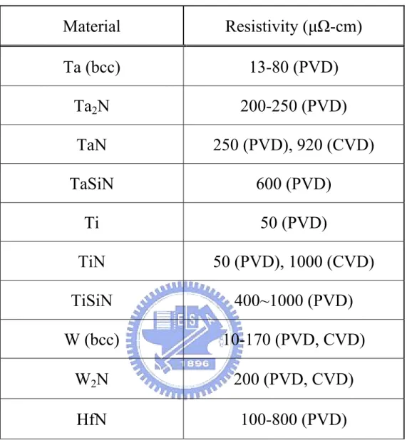
(22) 1.2 The choice of copper diffusion barrier Over the past few years, a considerable number of studies have been made on copper diffusion barriers [15]. In these studies, the refractory metal is the best choice as the barrier layer. Because the refractory metals do not miscible with the copper atom. So the TiN, TaN, Ta, TaSiN, TaO, Ta2N, W, WN, W2N, and TiSiN are choices to be the copper diffusion barrier [16]. The structure of TaSiN, TaO, and TiSiN is amorphous, and that of the others is crystallized [17]. In crystallized structure the copper will diffuse by the grain boundary which forms the fast diffusion path. For the thermal stability, the TaSiN and TiSiN can block the copper atoms diffusion up to 900°C, and make the diffusion path to become longer [18]. However, the resistivities of TaSiN and TiSiN are higher than other materials, and the crystallization of TaSiN and TiSiN will occur at high temperature. On the other hand, Ta and W have lower resistivity than TaSiN and TiSiN. But the sheet resistance of Ta and W will dramatically increase after 400°C annealing because of the diffusion of copper ions into the Si substrate [19]. And the structure of Ta and W are crystallized. The grain boundary will make copper diffuse across the barrier layer, even at low temperature situation [19]. We can add some impurities, such as nitrogen, oxygen, carbon or silicon to be the crystallization nuclear. When we add the impurities as the nuclear, the structure of the barrier layer will become amorphous or crystal structure with smaller grain. The fast diffusion path will be therefore eliminated. In addition to the thermal stability, the resistivity is an important parameter of the. 5.
(23) barrier layer. In Table 1-1, we list the resistivity of several materials which can be the copper diffusion barrier. As we had mentioned in above section, we must choose a barrier layer which have lower resistivity to reduce the effect of RC delay. There are two major methods to deposit the copper diffusion barrier: Physical Vapor Deposition (PVD) and Chemical Vapor Deposition (CVD). The diffusion barrier deposited by PVD method has many advantages, such as low cost, easy to fabricate, low resistivity, low impurity concentration, and high density [17]. But there are still one disadvantage using PVD method that is, the worse step coverage. When the dimension of integrated circuits is scaling down, the aspect ratio will be increased. Therefore, the PVD method will cause overhang to appear. As the deposition thickness increased, the overhang will seal the hole and keep a void in the hole. The void in the hole will induce the reliability reduce, and limit the scaling down of the dimension of integrated circuits [20]. The ionized physical vapor deposition (IPVD) and ionized metal plasma (IMP) have been brought up to modify this problem. When the dimension scales down to 0.13 µm, however, the improvement of these methods is restricted. The diffusion barrier deposited by CVD method has better step coverage than the barrier layer made by PVD method. The CVD method to fabricate the copper diffusion barrier is suitable for scaling down the dimension of integrated circuits [21]. But the process temperature of CVD method is higher than PVD method. Thus the CVD method is not easy to be integrated with back-end-of-line (BEOL) process. The MOCVD has lower process temperature than. 6.
(24) general CVD method. Nevertheless, the resistivity of MOCVD fabricated diffusion barrier is higher than that of the others. The ALD method to fabricate the diffusion barrier has been brought up in recent years [22]-[25]. The ALD method has the characteristic of ability to achieve nearly perfect conformity or step coverage. Using this technique, high quality films of superior conformity, in addition to uniform and precisely controlled thickness, can be deposited over various morphologies on a wafer [22].. 1.3 Motivation Hafnium nitride (HfN) is a famous material for metal gate MOSFETs in past few years [26]. Due to the larger negative heat of formation of HfN (-88.2 kcal/mol) compared with titanium nitride (TiN) (-80.4 kcal/mol) and tantalum nitride (TaN) (-60.3kcal/mol), it is expected that the thermal stability of HfN is better than TiN and TaN, and exhibit negligible variation for EOT on RTA treatments up to 1000°C. The work function of HfN is 4.65 eV, it is the mid-gap work function respect to silicon substrate and no obvious change after 1000°C RTA treatments. Mid-gap work function makes the application of HfN at n-type MOS structure or p-type MOS structure as gate electrode [27]. HfN also has many advantages such as excellent barrier against oxygen diffusive and leakage current stability makes it an ideal gate electrode for MOS device application [28]. But there is one problem using HfN as gate material of MOSFETs or MOS capacitors structure. That is the high sheet resistance of HfN.. 7.
(25) High sheet resistance will cause the RC delay becoming more serious. So we need a low resistance material capping on HfN to lowering the sheet resistance of gate. Copper is a low resistance material which is generally used as the interconnection to lower the effect of RC delay. Capping copper on HfN can effectively lower the sheet resistance of gate electrode. But the premise is HfN can block the copper atoms diffusion into the dielectrics and the silicon substrate. Because of the compact atomic structure, TaN and TiN are regularly used to be the copper diffusion barrier. The high density of HfN (13.8 g/cm3) is larger than that of TaN (13.7 g/cm3) and TiN (5.43 g/ cm3), which conforms to the requirement of copper diffusion barrier: excellent thermal stability, high melting point, and good adhesion [28]. So we use Cu as the electrode and HfN as the copper diffusion barrier to fabricate the MOS capacitor to investigate the copper diffusion barrier efficiency of HfN, the electric characteristics, and reliability of copper gate MOS capacitor.. 1.4 Organization of the Thesis The investigation includes five chapters. In chapter 1, we make an introduction to describe the issues of gate material we may meet during the dimensions scaling down. And we would talk about using Cu gate to overcome the problems we met in conventional polysilicon gate MOSCAPs. Then, the requirements of diffusion barrier layer to block Cu ions. 8.
(26) diffusion were discussed. In chapter 2, we will investigate the process procedures, measurement methods of electrical properties, and the methods of material analysis. In chapter 3, we will investigate the electrical properties and reliability of the Cu gate MOSCAPs with different thickness of HfN diffusion barrier. The electrical properties and reliability comparison of TaN and HfN diffusion barrier will discussed in this chapter, too. In chapter 4, we will investigate the thermal stability of Cu gate MOSCAPs with 28-nm-thick HfN diffusion barrier. The electrical properties and reliability of the MOSCAPs annealed in different annealing temperature will be compared in this chapter. Finally, in chapter 5, we will make a conclusion in the whole thesis. We will also recommend the best condition for the Cu gate MOSCAPs with HfN diffusion barrier.. 9.
(27) Chapter 2. Experimental Procedure. 2.1 Standard process Cu/HfN/SiO2/p-Si MOS capacitors (MOSCAPs) of an area of 4.45×10⁻⁴ cm2 were fabricated on 6-inch p-type (100)-oriented Si wafers, which with resistivity of 15-25 Ω-cm. Fig. 2-1 shows the key process flow of this structure. All wafers were initially cleaned by RCA (Radio Corporation of America) clean process. And 10-nm thermal gate oxide was subsequently deposited on the Si wafers by furnace at 925°C. Afterwards wafers were split into three groups. Different thickness of HfN films from 20 nm to 60 nm were then deposited on first group of the samples through the metal mask as the Cu diffusion barrier by sputtering. The sputtering condition is Ar/N2 = 60/1.5 sccm mixed gas ambient and at a sputtering DC power of 200 W. The total gas pressure was kept at 7.6×10⁻³ torr during the HfN sputtering process. Immediately, 300-nm-thick Cu was deposited on these samples as gate electrode. 34-nm-thick TaN film was deposited on the second group of the wafers, and the sputtering condition is in the same manner with the first group of wafers with HfN diffusion barrier. 300-nm-thick Cu film was subsequently deposited on TaN as the gate electrode. The Cu film is directly deposited on the last group of wafers as the control (no barrier) samples. Finally, all. 10.
(28) wafers received a 500-nm-thick Al deposition on the wafer backside by the thermal coater to form the ohmic contact.. 2.2 Thermal treatments Cu/HfN/SiO2/p-Si MOSCAPs with 28-nm-thick HfN were fabricated to study the thermal stability of the HfN diffusion barrier and the reliability of Cu gate MOSCAPs. After standard process, the Cu/HfN/SiO2/p-Si MOS capacitors were treated by furnace at 400~600°C for 30 minutes in N2 ambient.. 2.3 Measurements 2.3.1 Electrical measurements Capacitance-Voltage (C-V) characteristics were measured by the Agilent-4284A precision LCR system, and the equivalent oxide thickness (EOT) was estimated by the high frequency (100 KHz) capacitance versus voltage curves in the strong accumulation region. Current-Voltage (I-V) characteristics were measured by the Keithley Model 4200-SCS semiconductor characterization system.. 2.3.2 Time dependent dielectric breakdown (TDDB), lifetime & charge to breakdown (QBD) measurements. 11.
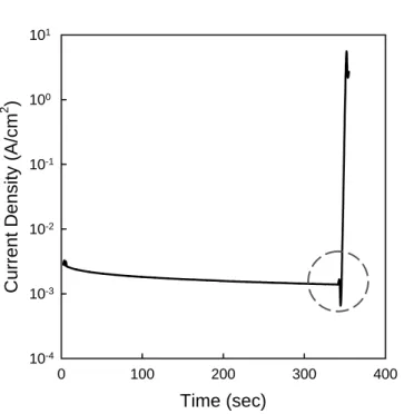
(29) Constant-Voltage-Stress (CVS) was conducted to evaluate reliability. The measurements were performed at room temperature, and the voltages of -13.6V, -13.9V, and -14.2V were applied to the capacitors. In Fig. 2-2, the dielectric breakdown was defined at the point which current density increases more than three orders of magnitude. The lifetime was extracted from the 63% of the time to breakdown in the CVS measurements with different voltages mentioned above. The QBD was calculated from the integrated current density before dielectric breakdown.. 2.3.3 Bias temperature stress (BTS) measurements To investigate the thermal stability of HfN films as the Cu diffusion barrier, BTS measurements were utilized to define the mobile ion quantity in the dielectric by the flat band voltage shift. The BTS measurements were performed at +1MV/cm for 1000 sec with temperatures of 50°C, 100°C, and 150°C.. 2.3.4 Elevated temperature measurements To investigate the conduction mechanism and the electrode work function variation of Cu/HfN/SiO2/p-Si MOSCAPs with 28-nm-thick HfN after different temperature treatments. I-V characteristics with various temperatures were measured at room temperature, 50°C, 75°C, 100°C, 125°C, and 150°C.. 12.
(30) 2.3.5 Material analysis Scanning Electron Microscopy (SEM) was used to determine the exact thickness of HfN diffusion barrier. Secondary-Ion-Mass-Spectrometer (SIMS) was used to evaluate the Cu diffusion barrier efficiency of the HfN films.. 13.
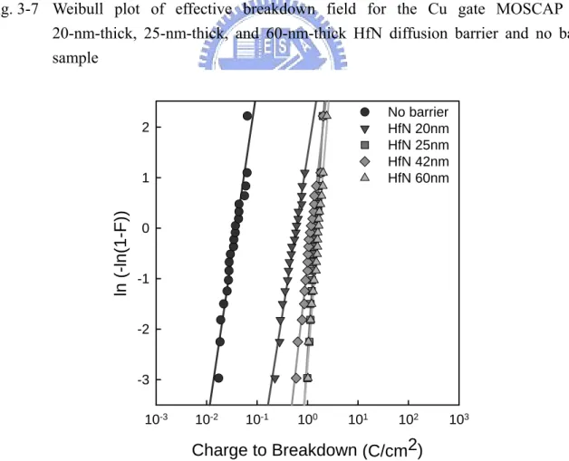
(31) Chapter 3. Electrical Characteristics and Reliability of Copper Gate MOSCAPs with HfN Diffusion Barrier. 3.1 Electrical characteristics of Cu gate MOSCAPs with different thickness of HfN Fig. 3-1 to Fig. 3-4 shows the SEM pictures of different thickness of HfN diffusion barrier. We can define the physical thicknesses of HfN diffusion barrier by these pictures as 20 nm, 25 nm, 42 nm, and 60 nm. Fig. 3-5 is the comparison of C-V curves for Cu gate MOSCAP with different thickness of HfN diffusion barrier. In this figure we can find an obviously flat band voltage shift between no barrier control sample and HfN diffusion barrier samples. The flat band voltage shift is caused by the work function difference of Cu and HfN. The ideal work function of Cu is about 5.1 eV and that of HfN is about 4.65 eV. The comparison of I-V curves of Cu gate MOSCAP with different thickness of HfN diffusion barrier is shown at Fig. 3-6. In this figure, we can find the leakage currents of different thickness of HfN diffusion barrier and no barrier control samples are almost at the same level around the low voltage bias region. But there seems a little difference at the region neighboring breakdown voltage. So we make a Weibull plot of effective breakdown field. 14.
(32) (EBD(eff)) in Fig. 3-7. In the Weibull plot, we can see that the absolute value of EBD(eff) distribution for no barrier control sample is larger than that for the other samples with HfN diffusion barrier. The EBD(eff) for Cu gate MOSCAPs with 20-nm-thick HfN diffusion barrier is smaller than that for Cu gate MOSCAPs with 25-nm-thick and 60-nm-thick HfN diffusion barriers. Cu diffusion into the dielectric and influence on the EBD(eff) are perhaps the reasons why the EBD(eff) for 20-nm-thick HfN is smaller than the other two samples. For no barrier control sample, the quantity of diffusion of Cu ions is random. Thus, the degree of influence of EBD(eff) for Cu ions is random in different MOSCAPs. By this reason, the EBD(eff) distribution of control sample in Weibull plot is larger than the other HfN diffusion barrier samples.. 3.2 Reliability of Cu gate MOSCAPs with different thickness of HfN The charge to breakdown was measured at applied biases of -13.6V, -13.9V, and -14.2V on the gate electrode. The exhibitions of charge to breakdown at these voltage biases are almost the same. So we compare the charge to breakdown for different thickness of HfN diffusion barrier at voltage biases of -13.6V. Fig. 3-8 is the Weibull plot of the charge to breakdown for Cu gate MOSCAPs with 20-nm-thick to 60-nm-thick HfN diffusion barriers and no barrier control sample. On the Weibull plot of the charge to breakdown for Cu gate. 15.
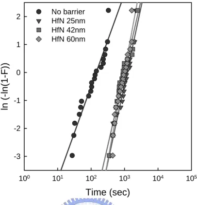
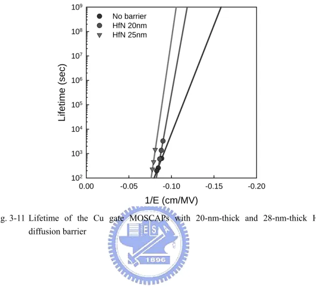
(33) MOSCAPs with 25-nm-thick to 60-nm-thick HfN diffusion barrier, the values of the charge to breakdown are almost the same. As to no barrier control sample, the charge to breakdown is apparently smaller than the other samples with HfN diffusion barrier. We can also find that the charge to breakdown for Cu gate MOSCAPs with 20-nm-thick HfN diffusion barrier is smaller than that for the Cu gate MOSCAPs with 25-nm-thick to 60-nm-thick HfN diffusion barrier. Fig. 3-9 shows the Weibull plot of TDDB of Cu gate MOSCAP with 25-nm-thick to 60-nm-thick HfN diffusion barrier and no barrier control sample. The electric field of -13.06 MV/cm was applied to the gate electrode to measure the TDDB characteristics. The TDDB exhibition of Cu gate MOSCAPs with 25-nm-thick to 60-nm-thick HfN diffusion barrier are almost the same. In Fig.3-10, the TDDB of Cu gate MOSCAP with 20-nm-thick and 28-nm-thick HfN diffusion barrier was compared. The TDDB characteristics were degraded at 20-nm-thick HfN diffusion barrier sample. Fig.3-11 shows the comparison of lifetime of Cu gate MOSCAPs with 20-nm-thick, 25-nm-thick HfN diffusion barrier, and no barrier control sample. The lifetime was measured at -13.6V, -13.9V, and -14.2V to make the Weibull plot of TDDB, and then the 63% of TDDB was selected to make the plot of lifetime. The 25-nm-thick HfN diffusion barrier sample shows better lifetime than the 20-nm-thick HfN diffusion barrier sample. The degradation of charge to breakdown and lifetime is perhaps due to the Cu diffusion into the dielectric. Cu ions are the positive charged mobile ion in dielectric layer. When the. 16.
(34) Cu ions diffuse into the dielectric along with a voltage applied on the electrode of the MOSCAPs, the Cu ions will move towards the cathode. The electric field between cathode and mobile ions will increase because of the shorter distance between Cu ions and cathode [29][30]. Then the current density between Cu ions and cathode will increase with the electric field. Larger current density will enhance the damage of dielectric and lower the charge to breakdown, TDDB, and lifetime of the MOSCAPs. Fig.3-12 to Fig.3-15 are SIMS analysis data of Cu gate MOSCAP with 20-nm-thick to 60-nm-thick HfN diffusion barrier and no barrier control sample. At first, the secondary ion counts of 20-nm-thick HfN diffusion sample and control sample were compared. The secondary ion counts of Cu in Si substrate for 20-nm-thick HfN diffusion barrier sample are apparently smaller than control sample. This result shows the HfN layer has the ability to block the Cu ions diffusion into the dielectric. Subsequently, we make a study of the barrier efficiency of Cu gate MOSCAPs with different thickness of HfN diffusion barrier. We compare the counts of Cu at the peak of silicon. For 20-nm-thick HfN diffusion barrier sample, the quantity of Cu counts is at 103 to 104 ions. The quantity of Cu counts is at 102 to 103 ions for 25-nm-thick to 60-nm-thick HfN diffusion barrier samples and is smaller than that for 20-nm-thick HfN diffusion barrier sample. It shows the barrier efficiency is almost the same when the thickness of HfN diffusion barrier is over 25-nm-thick, and is degraded when the thickness is down to 20-nm-thick. In these SIMS analysis data, the 25-nm-thick HfN has. 17.
(35) been determined to be a suitable thickness condition for HfN diffusion barrier.. 3.3 Comparison of HfN and TaN diffusion barrier TaN is a well-known material for the Cu diffusion barrier in recent years [31]-[33]. So we fabricate the Cu gate MOSCAPs with 34-nm-thick TaN diffusion barrier to compare with that with 28-nm-thick HfN diffusion barrier. The thicknesses of these samples are identified by the SEM shown in Fig.3-16 and Fig.3-17. Fig.3-18 shows the C-V curves of TaN and HfN diffusion barrier samples. Because of the work function differences between TaN (4.8eV) and HfN (4.65eV), we can observe the flat band shift in the C-V curve. The EOT of TaN and HfN diffusion barrier samples are 12.1 nm and 12.4 nm. I-V curves are shown in the Fig. 3.19. The leakage current density of TaN diffusion barrier sample is only a little lower than that of the HfN diffusion barrier one. In the electrical characteristics, the 34-nm-thick TaN and 28-nm-thick HfN samples are similar with each other. Fig.3-20 shows the Weibull plot of the charge to breakdown for HfN and TaN diffusion barrier samples measured at the voltage of -13.6 V applied on the gate electrode. We can find the charge to breakdown for the TaN diffusion barrier sample is smaller than that for the HfN diffusion barrier sample. The TDDB and lifetime comparison for HfN and TaN diffusion barriers are shown at Fig. 3-21 and Fig. 3-22, respectively. The TDDB and lifetime exhibitions for the HfN diffusion barrier sample are also better than that for the TaN one. In. 18.
(36) previous sections of this chapter, we found that the barrier efficiency can be defined by the reliability characteristics and this can be proved through SIMS analysis. Thus, the reliability for 28-nm-thick HfN diffusion barrier is better than that for 34-nm-thick TaN one. This also shows the barrier efficiency of 28-nm-thick HfN diffusion barrier is better than that of 34-nm-thick TaN one.. 3.4 Summary In this chapter, we present the electrical characteristics and reliability of Cu gate MOSFETs with different thickness HfN diffusion barrier, and show the HfN is suitable to be the Cu diffusion barrier. The reliability is almost the same when thickness of HfN diffusion barrier is over 25-nm-thick, and degraded when the thickness of HfN diffusion barrier down to 20-nm-thick. SIMS analysis data shows the lower secondary ion counts of Cu in Si substrate when we insert HfN diffusion barrier between Cu gate electrodes and dielectric, it can proof the HfN layer can block the Cu ions diffusion into dielectric. The SIMS analysis data also shows the better Cu diffusion barrier efficiency when the thickness of HfN diffusion barrier thicker than 25-nm-thick, and degraded when the thickness of HfN diffusion barrier down to 20-nm-thick. And we compare the HfN diffusion barrier with the TaN diffusion barrier. By the results we observe above, the reliability issue can be the index of barrier efficiency of Cu diffusion. 19.
(37) barrier. So we compare the Cu diffusion barrier efficiency of 34-nm-thick TaN and 28-nm-thick HfN diffusion barrier sample by the reliability. The 28-nm-thick HfN diffusion barrier sample shows better reliability than the 34-nm-thick TaN diffusion barrier sample. It means the barrier efficiency of 28-nm-thick HfN is better than 34-nm-thick TaN.. 20.
(38) Chapter 4. Thermal Stability of Copper Gate MOSCAPs with HfN Diffusion Barrier. 4.1 Electrical characteristics of annealed Cu/HfN/SiO2/p-Si Fig. 4-1 shows the sheet resistance for Cu gate MOSCAP with 28-nm-thick HfN diffusion barrier both as-deposited and after 400°C, 500°C, 600°C annealing in N2 ambient for 30 minutes. We can find an obvious sheet resistance difference between as deposited and after 400°C annealing samples. The sheet resistance was lowered down after 400°C annealing. This is because of the looser structure deposited by PVD, and the structure turns to be more compact after annealing. When the structure of electrode was changed after annealing, the work function of the electrode changed with the structure. The sheet resistance of Cu gate MOSCAP with 28-nm-thick HfN diffusion barrier did not change apparently for the samples after 400°C, 500°C, and 600°C annealing. It shows the work function of the electrode did not changed apparently for the samples received 400°C, 500°C, and 600°C annealing. The comparison of C-V curves was shown at Fig. 4-2. We can observe a positive flat band voltage shift between as deposited and after 400°C annealing samples. A negative flat band voltage shift was found for the samples after 600°C annealing in this figure compared. 21.
(39) with that after 400°C annealing. The positive flat band voltage shift may be due to the work function difference of the gate electrode and the elimination of the plasma induced oxide charge after annealing. The plasma induced oxide charge was generated during the deposition of the HfN layer and the Cu electrode through sputtering. The work function difference of gate electrode and the positive charge injection are the possible reasons causing the negative flat band voltage shift between 400°C and 600°C [34]. Fig. 4-3 shows the C-V measurement of as deposited sample at different frequencies. The frequencies for the C-V measurement are 1 K, 10 K, and 100 KHz. A hump was found at the depletion region for the C-V curves of 1 KHz and 10 KHz. The poorer interface state quality is the reason of the hump appeared in C-V curves [35]. After 400°C, 500°C, and 600°C annealing, the hump disappearance was found in the C-V curves at Fig. 4-4, Fig. 4-5, and Fig. 4-6, respectively. This implies the poorer interface state quality was annealed by 400°C, 500°C, and 600°C N2 ambient annealing. Fig. 4-7 is the C-V curves measured from +1 V to -6 V, and then from -6 V to +1 V immediately. A hysteresis of 100 mV can be observed in this plot. The major reasons to cause the hysteresis are the plasma induced oxide charges generated during the deposition of the HfN layer and the Cu electrode by sputtering. In Fig. 4-8, the hysteresis was eliminated when the Cu gate MOSCAP with 28-nm-thick HfN diffusion barrier was annealed at 400°C N2 ambient for 30 minutes. The elimination of the hysteresis means the plasma induced oxide. 22.
(40) charges have been removed at 400°C annealing. Fig. 4-9 and Fig. 4-10 show the C-V curves for the samples after 500°C and 600°C annealing, respectively. The hysteresis was not found in these annealing conditions as well as the 400°C annealing one. The comparison of I-V curves for as deposited, 400°C, 500°C, and 600°C annealed samples are shown in Fig. 4-11. We can find the leakage currents for 400°C, 500°C, and 600°C annealed samples are slightly lower than that for as deposited sample at low voltage regime. This is because the plasma induced oxide charges and the traps in SiO2 were removed and cured during annealing process. In high voltage region, the leakage currents for 500°C and 600°C annealed samples increase rapidly. That means the Cu ions diffuse into the dielectric and cause the increasing of the leakage currents dramatically. For 400°C annealed sample, the leakage current always keep lower level than that for as deposited one in whole range of voltage swept, which means the HfN barrier efficiency was good enough to block the Cu ions diffusion into the dielectric. In the I-V curves, we can also find that the breakdown voltage is increased after 400°C annealing and decreased after either 500°C or 600°C annealing. We make a Weibull plot of effective breakdown electric field for 400°C, 500°C, and 600°C annealed samples. We can observe that the effective breakdown voltage was increased after 400°C annealing and decreased with the higher annealing temperatures. The effective breakdown field distribution for 600°C annealed samples is larger than that for either 400°C or 500°C annealed samples. This result indicates that the Cu ions diffusion starts for. 23.
(41) the sample treated by 500°C for 30 minutes in N2 ambient, and turns to be more seriously when the sample treated by 600°C for 30 minutes in N2 ambient.. 4.2 Conduction mechanism of annealed Cu/HfN/SiO2/p-Si The Fowler-Nordheim (F-N) tunneling is the main conduction mechanism for MOSCAPs using SiO2 as the dielectric layer. The F-N tunneling is occurring at high voltage applied on the MOSCAPs, then the electron can transport across the potential energy barrier [36]. The equation of leakage current density is:. ⎛ −B ⎞ 2 J = AEOX exp ⎜ ⎟, ⎝ EOX ⎠. (1). 4 2m* 3 φB m0 q 3 , B= , and m0 is the mass of the electron, q is the charge where A = 16π 2 =m*φB 3q=. of the electron, = is the reduced Planck constant, m* is the effective mass, φB is the contact potential barrier, EOX is the applied electric field. The slope of the leakage current equation can be rearranged as:. B ⎛ J ⎞ = − ln ⎜ 2 ⎟ EOX ⎝ AE ⎠. (2). slope = B From the equations shown above, the leakage current behaviors of the insulated films can be investigated further on the leakage current density over the square of the electric field applied (J/E2) versus the reciprocal of the electric field (1/E) characteristics, i.e. ln (J/E2) vs. (1/E) 24.
(42) plots. The plot of the nature log of the leakage current density over the square of the applied electric field versus the reciprocal of the electric field was observed. It is found that the leakage current density over the square of the electric field is linearly related to the reciprocal of the applied electric field. When measuring the leakage current in different temperature, the difference of the leakage current was small at high electric field region. The barrier height is defined from the conduction band of the electrode to the conduction band of the dielectric. It can be determined from the slop of the ln (J/E2) vs. (1/E) plot. Fig. 4-13 to Fig. 4-16 show the ln (J/E2) – (1/E) curves of the as deposited, 400°C, 500°C, and 600°C annealed samples. The leakage current was measured at room temperature, 50°C, 75°C, 100°C, 125°C, and 150°C. We can find that (J/E2) is linearly related to (1/E) at high voltages region in these figures. The barrier height was fitted by the slope of the ln (J/E2) - (1/E) curve as shown in Fig. 4-17. Compared with that of the as deposited sample, the barrier height is obviously increased after 400°C annealing. In Fig. 4-18 and Fig. 4-19, we plot the band diagrams for the as deposited and the 400°C annealed samples. The increased barrier height means the work function of the gate electrode was increased after 400°C annealing compared with that of the as deposited sample. No obvious changes were observed on the barrier height of 400°C, 500°C, and 600°C annealed samples. It also means the work function of the Cu gate MOSCAP with 28-nm-thick HfN diffusion barrier have no obvious changes when the annealing temperature increases from 400°C to 600°C.. 25.
(43) In section 4.1 we have found the flat band voltage shift in C-V curves of as deposited, 400°C, 500°C, and 600°C annealed samples. According to the barrier height we extracted from the conduction mechanism, the positive flat band voltage shift between the as deposited and the 400°C annealed samples is partially due to the work function difference. The work function did not have appreciable changes for 400°C and 600°C annealed samples. That means the work function difference is not the reason why there are positive flat band voltage shift between 400°C and 600°C annealed sample. The barrier height, the work function, the flat band voltage and charges in dielectrics were recorded in Table 4-1. The charges within the dielectric include: oxide trapped charge, interface trapped charge, fixed oxide charge, and mobile ionic charge [37]. In Table 4-1 we can find the charges in dielectric were decreased to 1.36×10¹²/cm2 after 400°C annealing and then increased with the increased annealing temperature. The charges decreased after 400°C annealing means the plasma induced oxide charges have been removed by annealing. The charges in dielectric increased after 600°C annealing. This indicates the reason that causes the positive flat band voltage shift between 400°C and 600°C annealed samples is the positive charge injection. It means the Cu diffusion into the dielectric in regards to the positive charge injection for the Cu gate MOSCAPs with HfN diffusion barrier. Therefore, the barrier efficiency of HfN was lowered down.. 4.3 Bias temperature stress 26.
(44) The bias temperature stress is used to define the quantity of mobile ions in the dielectric and the thermal stability of Cu diffusion barrier [38]. The C-V curve was measured at room temperature initially, and then the temperature was raised. The temperatures used to stress the MOSCAP are ranging approximately from 150°C to 250°C. The electric field of +1MV/cm was applied to the gate electrode for 5 to 10 minutes. After bias-temperature stressing, cooling down of the sample was conducted rapidly, and the C-V curve was measured again at room temperature. The flat band shift in the plot of C-V curves before and after stressing reveals the quantity of mobile ions in the dielectric. The quantity of mobile ions is shown as:. Qm =. VFBshift Cox. (3). where Qm is the charge quantity of mobile ions, VFBshift is the flat band voltage shift before and after stressing, Cox is the maximum capacitance in the C-V curve. Fig. 4-19, Fig. 4-20, and Fig. 4-21 show the C-V curves of 400°C, 500°C, and 600°C annealing subjected to different stressing conditions, respectively. The stressing conditions comprise both raising the temperature to 50°C, 100°C, and 150°C and applying the field of +1MV/cm on the gate electrode for 1000 sec. Subsequently, the samples were cooled down and the C-V curves were again measured. We cannot find obvious flat band voltage shift among all curves for the 400°C annealed sample in Fig. 4-19. This shows the quantity of mobile ions is very small in the dielectric. In Fig. 4-20, the flat band voltage shift was not observed in the C-V curves for the samples before stressing and after 50°C bias-temperature 27.
(45) stressing. When the temperature of bias-temperature stressing was raised to 100°C and 150°C, however, the flat band voltage shift appeared. The flat band voltage shift for the 150°C bias temperature stressed sample is larger than that for the 100°C bias temperature stressed one. In Fig. 4-21, we can find obvious flat band voltage shift for all temperature conditions of bias temperature stressing. The comparison of flat band voltage shift for the 400°C, 500°C, and 600°C annealed samples are shown in Fig. 4-22. In this figure, we can find huge flat band voltage shift for the 600°C annealed sample and nearly no flat band voltage shift for the 400°C annealed sample. This shows the Cu ions diffusion into the dielectric for the 600°C annealed sample is more serious than that for the 400°C annealed sample. And the thermal stability for the Cu gate MOSCAP with 28-nm-thick HfN diffusion barrier receiving 400°C furnace annealing in N2 ambient for 30 minutes is better than that receiving 600°C furnace annealing in N2 ambient for 30 minutes. For the 500°C annealed sample, the flat band voltage shift was increased when the temperature of bias-temperature stressing is larger than 100°C also means the worse thermal stability and barrier efficiency when the Cu gate MOSCAPs with 28-nm-thick HfN diffusion barrier receiving 500°C furnace annealing in N2 ambient for 30 minutes.. 4.4 Reliability Fig. 4-23 is the Weibull plot of the charge to breakdown for Cu gate MOSCAP with. 28.
(46) 28-nm-thick HfN diffusion barrier with regard to as-deposition, 400°C, 500°C, and 600°C annealing. The charge to breakdown was measured at the bias of -13.6V, -13.9V, and -14.2V applied on the gate electrode. The exhibitions of charge to breakdown at these voltage bias conditions are almost the same. So we compare the charge to breakdown for the samples with different annealing temperature at the applied voltage of -13.6V. In the Weibull plot of the charge to breakdown for the as-deposited and the 400°C annealed samples, the values of the charge to breakdown are almost the same. However, the value of the charge to breakdown is decreased with annealing temperature. The slope for the 600°C annealed sample in the Weibull plot is larger than that for the other two annealed ones. Fig. 4-24 shows the Weibull plot of TDDB for the Cu gate MOSCAP with 28-nm-thick HfN diffusion barriers with regard to as-deposition, 400°C, 500°C, and 600°C annealing. An electric field of -12.82MV/cm was applied for the gate electrode to measure the TDDB characteristics. A slightly decrease can be seen when the annealing temperature was increased. Fig. 4-25 shows the lifetime for the as-deposited, 400°C, 500°C, and 600°C annealed samples. The lifetime was measured at -13.6V, -13.9V, and -14.2V to depict the Weibull plot of TDDB. The 63% of TDDB was selected to depict the plot of lifetime. In Fig. 4-25, we can find that the lifetimes for the as-deposited sample and after 400°C annealed sample are almost the same. But the lifetime was degraded for the samples receiving either 500°C or 600°C annealing.. 29.
(47) At chapter two, we showed the degradation of the charge to breakdown and lifetime, which means the barrier efficiency of HfN layer was lowered down and the Cu diffusion into the dielectric occurred. Therefore, it implies the 28-nm-thick HfN barrier efficiency was not degraded after 400°C annealing with respect to almost the same charge to break down and lifetime. For the 500°C annealed sample, a little degradation of charge to breakdown and lifetime was observed. This result indicates the barrier efficiency of the 500°C annealed 28-nm-thick HfN diffusion barrier starts to lower down, and a small amount of Cu ions diffuses into the dielectric. When the annealing temperature was increased to 600°C, a great degradation of charge to breakdown and lifetime was observed. That shows the 600°C annealed sample has larger number of Cu ions diffusion into the dielectric than the 500°C annealed one. The main reason of the HfN barrier efficiency lowering down maybe is the structure changes after annealing. The structure of the as-deposited HfN layer is amorphous. When we increase the annealing temperature, the grain size of the HfN diffusion barrier will become larger than that with lower temperature annealing. With the increased grain size, the quantity of fast diffusion path will be increased and the barrier efficiency will be lowered down.. 4.5 Summary In this chapter, we investigate the thermal stability of the Cu gate MOSCAPs with. 30.
(48) 28-nm-thick HfN diffusion barrier. For the sample with 400°C annealing in N2 ambient for 30 minutes, a positive flat band voltage shift has been found related with the as-deposited sample. By the change of sheet resistance and extracted barrier height from the conduction mechanism fitting, the positive flat band voltage shift is due to the work function difference of gate electrode and the plasma induced oxide charge removal by annealing. After bias-temperature stressing, obvious flat band shift was not found up to 150°C means the quantity of mobile ions in dielectric is small. The reliability issues for the Cu gate MOSCAP with 28-nm-thick HfN diffusion barrier after 400°C annealing are almost the same compared with that for the as deposited sample. As the results we mentioned above, 400°C annealing in N2 ambient for 30 minutes is a suitable annealing condition. For the samples after 500°C annealing in N2 ambient for 30 minutes, we found a flat band voltage shift after BTS with the temperature increased to 100°C and above. It means the barrier efficiency lowering and the mobile ion injection into the dielectric. The degraded reliability issues show the same results. For the samples after 600°C annealing in N2 ambient for 30 minutes, the Cu diffusion into the dielectric was observed through a flat band voltage shift after BTS and a negative flat band voltage shift in the C-V curve related with 400°C annealed sample. The worse reliability also indicates the Cu diffusion into the dielectric. So, it will cause the degradation of the barrier efficiency of HfN and not suitable for the Cu gate MOSCAPs with either 500°C or 600°C annealing in N2 ambient for 30 minutes.. 31.
(49) Chapter 5. Conclusions. HfN, deposited by PVD, is suitable to be the diffusion barrier of Cu. As compared with TaN, the well-known material to be the Cu diffusion barrier, HfN shows the better reliability. When the thickness of HfN is over 25 nm, the electrical characteristics and reliability are almost unchanged. We can observe the barrier efficiency of Cu gate MOSCAP with over 25-nm-thick HfN diffusion barrier through the SIMS analysis. When the thickness of HfN diffusion barrier is down to 20 nm, the reliability and the barrier efficiency were lowered down. Thus, 25 nm is a suitable thickness condition for HfN to be the Cu diffusion barrier. For the Cu gate MOSCAP with 28-nm-thick HfN diffusion barrier receiving 400°C furnace annealing in N2 ambient for 30 minutes, we can find a positive flat band voltage shift compared with that for the as-deposited sample. Through the changed sheet resistance and extracted barrier height from the conduction mechanism fitting, the positive flat band voltage shift is due to the work function difference of the gate electrode and the plasma induced oxide charge removal by annealing. After bias-temperature stressing, obvious flat band voltage shift was not found up to 150°C. This implies the quantity of mobile ions in the dielectric is small. The reliability issues for the Cu gate MOSCAP with 28-nm-thick HfN diffusion barrier after. 32.
(50) 400°C annealing is almost identical with that for the as-deposited sample. As the results we mentioned above, 400°C annealing in N2 ambient for 30 minutes is a suitable annealing condition. For the samples with either 500°C or 600°C annealing in N2 ambient for 30 minutes, we found visible flat band voltage shifts after bias-temperature stressing. It implies the barrier efficiency lowered and the mobile ion injection into the dielectric occurred. The same results were shown in the degraded reliability issues. For the sample with 600°C annealing in N2 ambient for 30 minutes, the Cu diffusion into the dielectric was observed through a negative flat band voltage shift in the C-V curve compared with that for the 400°C annealed sample. Therefore, either 500°C or 600°C annealing in N2 ambient for 30 minutes will cause the degraded barrier efficiency of HfN diffusion barrier such as to not suitable for HfN to be the Cu diffusion barrier in the Cu gate MOSCAPs.. 33.
(51) References. [1] J. Pan et al., “A low temperature metal-doping technique for engineering the gate electrode of replacement metal gate CMOS transistor,” IEEE Electron Device Lett., vol. 24, No. 9, p. 547, Sep., 2003. [2] J.M. Hergenrother et al., “50 nm Vertical Replacement-Gate (VRG) nMOSFETS with ALD HfO2 and Al2O3 gate dielectrics,” IEEE IEDM Tech. Dig., p. 3.1.1, 2001. [3] B. Guillaumot et al., “75 nm damascene metal gate and high-k integration for advanced CMOS devices,” IEEE IEDM Tech. Dig., p. 355, 2002. [4] H.S.P. Wang et al., “Beyond the conventional transistor,” IBM J. Res. Develop., vol. 46, p. 1332, 2002. [5] N.D. Arora et al., “Modeling the poly-silicon depletion effect and its impact on sub-micrometer CMOS circuit performance,” IEEE Trans. Electron Devices, vol. 42, p. 935, 1995. [6] Bin Yu et al., “Gate engineering for performance and reliability in deep-submicron CMOS technology,” in Symposium VLSI Tech., p. 105, 1997. [7] S.P. Murarka et al., “Advanced materials for fature interconnections of the future need and strategy,” Microelectronic Engineering, 37/38, p. 29, 1997 [8] The International Technology Roadmap for Semiconductors, Semiconductor Industry. 34.
(52) Association, San Jose, CA, p. 123, 1999. [9] J.R. Pfiester et al., “The effects of boron penetration on p+ poly-silicon gated PMOS devices,” IEEE Trans. Electron Devices, vol. 37, p. 1842, 1990. [10] B.-Y. Tsui et al., “Investigation of Cu/TaN metal gate for metal-oxide-silicon devices,” J.. Electrochem. Soc., 150 (1), p. G22, 2003. [11] J.T. Yue, “Reliability,” in ULSI Technology, McGraw-Hill, USA, p. 656, 1996. [12] B.J. Howard et al., “Reactive ion etching of copper in SiCl4 based plasmas,” Appl. Phys.. Lett., 59, p. 914, 1991. [13] J.O. Olowolafe et al., “Interdiffusions in Cu/reactive-ion-sputtered TiN, Cu/chemicalvapor-deposited TiN, Cu/TaN, and TaN/Cu/TaN thin-film structures: low temperature diffusion analyses,” J. Appl. Phys., vol. 72, No. 9, p. 4099, Nov, 1992. [14] M.-A. Nicolet et al., “Diffusion barrier in thin film,” Thin Solid Films, 52, p. 415, 1978. [15] T. Laurila, “Tantalum based diffusion barriers for copper metallization,” Thesis of. Helsinki University of Technology, 2001. [16] S.-Q. Wang et al., “Diffusion barriers properties of TiW between Si and Cu,” J. Appl.. Phys., 73, p. 2301, 1993. [17] W.-H. Wu, “Tungsten-Rhenium alloy (ReW3) thin films as diffusion barrier for Cu metallization on Si/SiO2 substrates,” Thesis of Materials Science and Engineering,. NCTU, 2003.. 35.
(53) [18] E. Blanquet et al., “Evaluation of LPCVD Me-Si-N (Me=Ta, W, Re) diffusion barriers for Cu metallizations,” Microelectronic Engineering, 37/38, p. 189, 1997 [19] H. Ono et al., “Diffusion barrier effects of transition metals for Cu/M/Si multi-layers,”. Appl. Phys. Lett., 64(12), p. 1511, 1994. [20] H. S. Choe et al., “MOCVD TiN diffusion barriers for copper interconnects,” IEEE IITC, p. 62, 1999. [21] S. C. Sun et al., “A comparative study of CVD TaN diffusion barrier for copper interconnection,” IEEE IEDM Tech. Dig., p. 461, 1995. [22] C. H. Peng et al., “A 90nm generation copper dual damascene technology with ALD TaN barrier,” IEEE IEDM Tech. Dig., p. 603, 2002. [23] M. Juppo et al., “Use of 1,1-Dimethylhydrazine in the atomic layer deposition of transition metal nitride thin films,” J. Electrochem. Soc. 147, p. 3377, 2002. [24] J.S. Park et al., “Plasma-enhanced atomic layer deposition of tantalum nitrides using hydrogen radicals as a reducing agent,” Electrochem. Solid State Lett., 4, p. C17, 2001. [25] J.W. Klaus et al., “Atomically controlled growth of tungsten and tungsten nitride using sequential surface reactions,” Appl. Surf. Sci, 162-163, p. 479, 2000. [26] H.Y. Yu et al., “Robust HfN metal gate electrode for advanced MOS devices application,” in Symposium VLSI Tech., p. 151, 2003. [27] H.Y. Yu et al., “Physical and electrical characteristics of HfN gate electrode for advanced. 36.
(54) MOS devices”, IEEE Electron Device Lett., p. 230, 2004. [28] H. Y. Yu et al., “Thermally robust HfN metal as a promising gate electrode for advanced MOS device applications,” IEEE Trans. Electron Devices, vol. 51, No. 4, Apr., p. 609, 2004. [29] S. Wolf et al., “Silicon processing for the VLSI era,” Lattice Press, vol. 3, p. 459. [30] Y.H. Lin et al., “The strong degradation of 30 Å gate oxide integrity contaminated by copper,” J. Electrochem. Soc., 148, p. F73, 2001. [31] W.-F. Wu et al., “Effects of nitrogen plasma treatment on tantalum diffusion barriers in copper metallization,” J. Electrochem. Soc., 150, p. G83, 2003. [32] H.-H. Hsu et al., “Displacement activation of tantalum diffusion barrier layer for electroless copper deposition,” J. Electrochem. Soc., 148, p. C590, 2001. [33] S.-L. Cho et al., “Diffusion barrier properties of metallorganic chemical vapor deposited tantalum nitride films against Cu metallization,” J. Electrochem. Soc., 146, p. 3724, 1999. [34] J. Westlinder et al., “On the thermal stability of atomic layer deposited TiN as gate electrode in MOS devices,” IEEE Electron Device Lett., vol. 24, No. 9, p. 550, 2003 [35] S.-W. Huang et al., “Electrical characterization and process control of cost-effective high-k aluminum oxide gate dielectrics prepared by anodization followed by furnace annealing,” IEEE Trans. Electron Devices, vol. 50, No. 7, p. 1658, 2003.. 37.
(55) [36] D.K. Schroder, “Semiconductor material and device characteristics,” John Wiley & Sons,. Inc., p. 391. [37] S. M. Sze, “Physics of semiconductor devices,” Ch. 7, p. 380, Wiley, New York, 1981. [38] D.K. Schroder, “Semiconductor material and device characteristics,” John Wiley & Sons,. Inc., p. 365.. 38.
(56) Table 1-1 The resistivity of various barrier layers. Material. Resistivity (µΩ-cm). Ta (bcc). 13-80 (PVD). Ta2N. 200-250 (PVD). TaN. 250 (PVD), 920 (CVD). TaSiN. 600 (PVD). Ti. 50 (PVD). TiN. 50 (PVD), 1000 (CVD). TiSiN. 400~1000 (PVD). W (bcc). 10-170 (PVD, CVD). W2N. 200 (PVD, CVD). HfN. 100-800 (PVD).
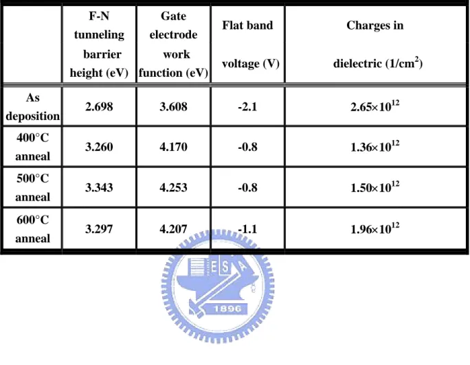
(57) Table 4-1 Comparison of barrier height, work function, flat band, and charge concentration under gate injection for the as deposited, 400ºC, 500ºC, and 600ºC annealed Cu/HfN/SiO2/p-Si MOSCAPs with 28-nm-thick HfN diffusion barrier. F-N tunneling. Gate electrode. barrier work height (eV) function (eV). Flat band. Charges in. voltage (V). dielectric (1/cm2). As deposition. 2.698. 3.608. -2.1. 2.65×10¹². 400°C anneal. 3.260. 4.170. -0.8. 1.36×10¹². 500°C anneal. 3.343. 4.253. -0.8. 1.50×10¹². 600°C anneal. 3.297. 4.207. -1.1. 1.96×10¹².
(58) A A X B. Fig. 1-1. B. The barrier layer X is between material A and B. A. A Interfacial layer Interfacial layer. B. (a). B. (c). B. (b). A X. ...... X. X. A No reaction between layer X and A or B. X. Amorphous. B. (d). Fig. 1-2 (a) sacrificial barrier, (b) stuffed barrier, (c) passive compound barrier, (d) amorphous barrier..
(59)
(60) 2. Current Density (A/cm ). 101. 100. 10-1. 10-2. 10-3. 10-4 0. 100. 200. 300. 400. Time (sec). Fig. 2-2 Dielectric breakdown was defined at the point which current density increases more than three orders of magnitude..
(61) 20 nm. Fig. 3-1 SEM picture of 20-nm-thick HfN diffusion barrier. 25 nm. Fig. 3-2 SEM picture of 25-nm-thick HfN diffusion barrier.
(62) 42 nm. Fig. 3-3 SEM picture of 42-nm-thick HfN diffusion barrier. 60 nm. Fig. 3-4 SEM picture of 60-nm-thick HfN diffusion barrier.
(63) 1.2. HfN 20nm HfN 25nm HfN 42nm HfN 60nm No barrier. Normalized Capacitance. 1.0. 0.8. 0.6. 0.4. 0.2. 0.0 -5. -4. -3. -2. -1. 0. 1. Applied Voltage (V) Fig. 3-5 C-V curves for the Cu gate MOSCAPs with 20-nm-thick, 25-nm-thick, 42-nm-thick, and 60-nm-thick HfN diffusion barrier and no barrier sample 102 101. 2. Current Density (A/cm ). 100 10-1. HfN 20nm HfN 25nm HfN 60nm No barrier. 10-2 10-3 10-4 10-5 10-6 10-7 10-8 10-9 10-10 10-11 10-12 0. -5. -10. -15. -20. -25. Applied Voltage (V) Fig. 3-6 I-V curves for the Cu gate MOSCAPs with 20-nm-thick, 25-nm-thick, 42-nm-thick, and 60-nm-thick HfN diffusion barrier and no barrier sample.
(64) 3 HfN 20nm HfN 25nm HfN 60nm No barrier. 2. ln (-ln(1-F)). 1 0 -1 -2 -3 -4 6. 8. 10. 12. 14. 16. Effective Breakdown Field (MV/cm) Fig. 3-7 Weibull plot of effective breakdown field for the Cu gate MOSCAP with 20-nm-thick, 25-nm-thick, and 60-nm-thick HfN diffusion barrier and no barrier sample No barrier HfN 20nm HfN 25nm HfN 42nm HfN 60nm. 2. ln (-ln(1-F)). 1. 0. -1. -2. -3 10-3. 10-2. 10-1. 100. 101. 102. 103. Charge to Breakdown (C/cm2) Fig. 3-8 Weibull plot of charge to breakdown for the Cu gate MOSCAPs with 20-nm-thick, 25-nm-thick, 42-nm-thick, and 60-nm-thick HfN diffusion barrier and no barrier sample.
(65) 2. ln (-ln(1-F)). 1. No barrier HfN 25nm HfN 42nm HfN 60nm. 0. -1. -2. -3 100. 101. 102. 103. 104. 105. Time (sec) Fig. 3-9 The Weibull plot of TDDB at 13.06 MV/cm for the Cu gate MOSCAPs with 20-nm-thick to 60-nm-thick HfN diffusion barrier and no barrier control samples 3. HfN 20nm HfN 28nm. 2. ln (-ln(1-F)). 1 0 -1 -2 -3 -4 102. 103. 104. Time (sec) Fig. 3-10 The Weibull plot of TDDB at 12.82 MV/cm for the Cu gate MOSCAPs with 20-nm-thick and 28-nm-thick HfN diffusion barrier.
(66) 109 108. No barrier HfN 20nm HfN 25nm. Lifetime (sec). 107 106 105 104 103 102 0.00. -0.05. -0.10. -0.15. -0.20. 1/E (cm/MV) Fig. 3-11 Lifetime of the Cu gate MOSCAPs with 20-nm-thick and 28-nm-thick HfN diffusion barrier.
(67) 107 O Si Cu. Secondary ion counts. 106 105 104 103 102 101 100 0. 200. 400. 600. 800. 1000 1200 1400. Sputtering time (sec) Fig. 3-12 SIMS analysis of the Cu gate MOSCAPs without diffusion barrier 107. N O Si Cu Hf. Secondary ion counts. 106 105 104 103 102 101 100 0. 200. 400. 600. 800. 1000. 1200. Sputtering time (sec) Fig. 3-13 SIMS analysis of the Cu gate MOSCAPs with 20-nm-thick HfN diffusion barrier.
(68) 107. N O Si Cu Hf. Secondary ion counts. 106 105 104 103 102 101 100 0. 200. 400. 600. 800. 1000 1200 1400. Sputtering time (sec) Fig. 3-14 SIMS analysis of the Cu gate MOSCAPs with 25-nm-thick HfN diffusion barrier 107. N O Si Cu Hf. Secondary ion counts. 106 105 104 103 102 101 100 0. 200. 400. 600. 800. 1000 1200 1400. Sputtering time (sec) Fig. 3-15 SIMS analysis of the Cu gate MOSCAPs with 60-nm-thick HfN diffusion barrier.
(69) 28 nm. Fig. 3-16 SEM picture of 28-nm-thick HfN diffusion barrier. 34 nm. Fig. 3-17 SEM picture of 34-nm-thick TaN diffusion barrier.
(70) 1.2 HfN 28nm TaN 34nm. Normalized Capacitance. 1.0. 0.8. 0.6. 0.4. 0.2. 0.0 -5. -4. -3. -2. -1. 0. 1. Applied Voltage (V) Fig. 3-18 The C-V curves for Cu gate MOSCAPs with 28-nm-thick HfN and 34-nm-thick TaN diffusion barrier 102 101. Current Density (A/cm2). 100. HfN 28nm TaN 34nm. 10-1 10-2 10-3 10-4 10-5 10-6 10-7 10-8 10-9 10-10 10-11 10-12 0. -5. -10. -15. -20. -25. -30. Applied Voltage (V) Fig. 3-19 The I-V curves for Cu gate MOSCAPs with 28-nm-thick HfN and 34-nm-thick TaN diffusion barrier.
(71) No barrier HfN 28nm TaN 34nm. 2. ln (-ln(1-F)). 1. 0. -1. -2. -3 10-3. 10-2. 10-1. 100. 101. 102. 103. Charge to Breakdown (C/cm2) Fig. 3-20 The charge to breakdown for Cu gate MOSCAPs with 28-nm-thick HfN and 34-nm-thick TaN diffusion barrier 3 HfN 28nm TaN 34nm 2. ln (-ln(1-F)). 1 0 -1 -2 -3 -4 102. 103. 104. Time (sec) Fig. 3-21 TDDB of the Cu gate MOSCAPs with 28-nm-thick HfN and 34-nm-thick TaN diffusion barrier.
(72) 109 108. HfN 28nm TaN 34nm. Lifetime(sec). 107 106 105 104 103 102 101 100 0.00. -0.05. -0.10. -0.15. -0.20. 1/E (cm/MV) Fig. 3-22 Lifetime of the Cu gate MOSCAPs with 28-nm-thick HfN and 34-nm-thick TaN diffusion barrier.
數據
+7
相關文件
The difference resulted from the co- existence of two kinds of words in Buddhist scriptures a foreign words in which di- syllabic words are dominant, and most of them are the
(Another example of close harmony is the four-bar unaccompanied vocal introduction to “Paperback Writer”, a somewhat later Beatles song.) Overall, Lennon’s and McCartney’s
專案執 行團隊
Cultivating a caring culture and nurturing humanistic qualities Building an ever-Learning School.. Targets Leading Key
Microphone and 600 ohm line conduits shall be mechanically and electrically connected to receptacle boxes and electrically grounded to the audio system ground point.. Lines in
volume suppressed mass: (TeV) 2 /M P ∼ 10 −4 eV → mm range can be experimentally tested for any number of extra dimensions - Light U(1) gauge bosons: no derivative couplings. =>
Courtesy: Ned Wright’s Cosmology Page Burles, Nolette & Turner, 1999?. Total Mass Density
• Formation of massive primordial stars as origin of objects in the early universe. • Supernova explosions might be visible to the most
