2004 IEEE Asia-Pacific Conference on Advanced System Integrated Circuits(AP-ASIC2004)I Aug. 4-5,2004
14-4
A 3.1-10.6
GHz CMOS Cascaded Two-stage Distributed Amplifier
for Ultra-Wideband Application
Kuan-Hung Chen and Chomg-Kuang Wang
Graduate Institute of Electronics Engineering, and Department of Electrical Engineering, National Taiwan University, 106 Taipei, Taiwan R. 0. C.
E-mail: ckwang@cc.ee.ntu.edu.tw
ABSTRACT
In this paper, a CMOS cascaded two-stage distributed amplifier for ultra-wideband (UWB) application is presented. The circuit using two-stage cascaded topology achieves better gain-bandwidth product performance than conventional CMOS distributed amplifiers. The simulated gain is 18dB with + l d B gain flatness over 3.1-10.6 GHz hands. Input and
output are matched to 50Q, and the retum losses of input and output are below -10dB and -9dB respectively. The power dissipation is 54mW with 1.8V power supply. The circuit was
fabricated in 0. IS-pm 1 P6M RF CMOS process.
I. INTRODUCTION
UWB is an emerging technology for wireless communication. Unlike narrow-band system, UWB has capability for high data rate communication applications, such as imaging systems, vehicular radar systems, and ground penetrating [I]. Although the standard of UWB has not been finalized, many proposed researches target at the band between 3.1 and 10.6 GHz. In this work, the design goal is to
achieve an amplifier with gain of 18dB over 3.1 to 10.6 GHz
Distributed amplification, characterized by wide bandwidth, has been prevalent over sixty years. Lots of distributed amplifiers are fabricated on the compound semiconductor processes for applications of mini-meter wave. However, the CMOS technology is less expensive than compound semiconductor processes and has higher potential for integration with the digital part, especially for silicon-on-chip solutions. Researches on the CMOS distributed amplifiers have made considerable progress in the recent years.
Of these researches, one accomplished a gain of 5
*
1.2dB from 300 kHz to 3 GHz, and 4.7 GHz unity-gain cutofffrequency [2]. In another work, a 0.5 to 8.5 GHz CMOS fully differential distributed amplifier was realized with a gain of
5 . 5 i 1.5dB in a 0.6-pm CMOS process [4]. Lastly, a 0.5 to 14 GHz with 10.6 i 0.9dB gain and a 0.6 to 22 GHz with 7.3 i 0.8dB gain distributed amplifier using 0.18-pn CMOS RF process were proposed [7]-[8]. Among these, amplifier’s gain does not exceed 10.6dB, which is not high enough for advance applications, such as UWB system. The cascaded [ W .
This work was supported in part by Media Tek Inc. Hsin Chu,
Taiwan 300.
0-7803-8637-X/04/$20.00~2004
IEEE.
single-stage distributed amplifier (CSDA) topology was brought out for increasing the amplifier’s gain [ 6 ] . In that work, the CSDA has 21dB gain and 5 GHz bandwidth but the
CSDA needs more complicated dc-wise setup than conventional distributed amplifiers.
In this paper, a cascaded two-stage distributed amplifier (CTDA) is proposed, and it possesses the high gain property of CSDA without complicate dc-wise setup. This paper is organized as follows. Some basics of the conventional distributed amplifier design are described in Section II.
Section 111 covers the topology of CTDA and some comparisons between the conventional distributed amplifier, CSDA and CTDA. Section IV shows the simulation results,
and conclusions are given in section V.
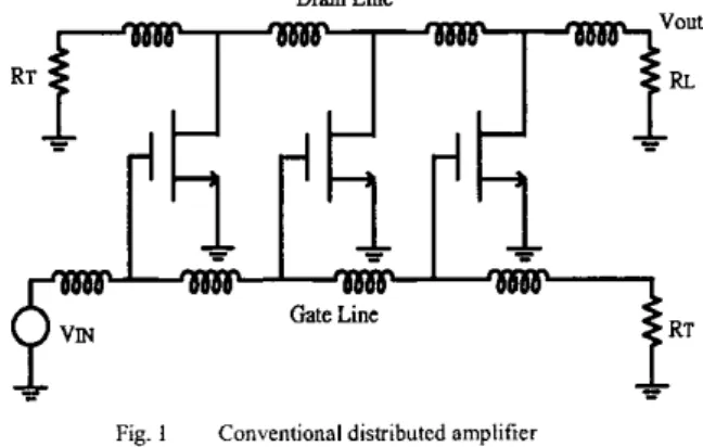
Drsin Line
f
f
Fig. 1 Conventional diseibutcd amplifier
11. BASICS OF DISTRIBUTED AMPLIFIER DESIGN Distributed amplifiers employ the topology that several gain stages are in parallel and series-inductors are introduced to separate capacitances of the input and output node of adjacent gain stages. This topology builds two artificial transmission lines, gate line and drain line. Output current is combined additively by the current flowing from each gain stage. The additive characteristic results in a relatively low gain, while the distributed nature of capacitance can achieve very wide bandwidth. Fig. I shows a thee-stage conventional distributed amplifier. Design equations can be referred to [IO],
[l I]. The voltage gain can be written as [ l l ] :
2004 IEEE Asia-Pacific Conference o n Advanced System Integrated Circuits(AP-ASIC2004)I Aug. 4-5,2004
(6.4 -
oz 1
-:(aliap) s i d N2 p
In [ 6 ] , the CSDA is proposed to enhance its gain. Assuming all the load resistance of each gain stage are the same, the equation of gain is:
(1) (8, - 6 8
1
sinh_ _
A , = - 2 where N number of stages;g, gain stage transconductance;
U ,
b',
Od propagation constant ofdrain line; cutoff frequency of transmission lines: propagation constant of gate line;
The cutoff frequency (wJ of transmission line is 2/=. It can be derived that voltage gain becomes maximum when
e,=
6,, as shown in Fig. 2. The more the propagation constant of the gate line differs from that of drain line, the more the amplifier gain decays.
3 1 2 1 1 1 5 I t 2 2 2 z1 I 6 I& 1
(2)
When
O,=
Hd, the equation of voltage gain can be simplified Fig. 2 Normalized gain VB. Ratio of B,and Bras:
' g -
A , = -
2 J ; - 0 '
Intuitively, the voltage gain can he enhanced when large N
is selected. Because the transmission lines are not ideal, some parasitic effects such as spiral inductor parasitic resistance make the propagation constant not purely imaginary, which leads to path loss. The voltage gain is not proportional to the number of stages anymore but achieves a maximum when the optimal value of N is used. The equation of optimal N is written as [ I I]:
(3)
where
6, real pari of propagation constant of gate line;
S,,, real part of propagation constant of drain line; For CMOS process, the
Nep,
is between 3 to 5 . This is one of the substantial reasons that distributed amplifier gain can not be large.(4)
where
N number of stages cascaded; g, gain stage transconductance; Ro
This is a novel approach to increase the gain of the amplifier. The gain grows in proportional to the power of N. However, if the gain of each stage ( g m . ~ , / 2 ) is not large, the amplifier gain can not grow very fast. In addition, extra components such as RF chock may be needed to setup dc operating voltage at each inter-connected node.
Therefore, we propose the cascaded two-stage distributed amplifier (CTDA) to solve these problems. Next session discusses the CTDA circuit topology.
output resistance of each stage;
Fig. 3 Cascaded WO-stage distributed amplifier
111. CTDA TOPOLOGY AND GAIN ENHANCEMENT The CTDA circuit topology is shown in Fig. 3. It could be regarded as two conventional two-stage distributed amplifiers cascaded. AC coupling capacitor is used for connecting these two conventional distributed'amplifiers and DC setup can be accomplished in the same way as that of conventional distributed amplifier. The cascode gain cell configuration is used for its high maximum available gain, better input-output isolation, and high output impedance [8]. The gain of CTDA can he written as:
where
N number of two-stage distributed amplifier cascaded;
2004 IEEE Asia-Pacific Conference on Advanced System Integrated Circuits(AP-ASIC2004)i Aug. 4-5,2004
Power Supply Frequency
Gain(& I)
Input Return loss(SII) Output Retum loss(Sz2)
Isolation(Slz) Noise Figure Power Consumption
Area Assuming conventional distributed amplifier, CSDA and
CTDA are all composed of four gain stages, the demanded transconductance per gain stage can be plotted respectively in different required gain, as shown in Fig. 4. When required gain is between 12dB-24dB, the transconductance of CTDA circuit is usually in proportion to the needed transconductance
~~ ~~
is the smallest among three of them. Power dissipation of the
IdB1
. . . . . .per gain-stage, so CTDA consumes the least power. ~ ~.~ . . . . . . . . .
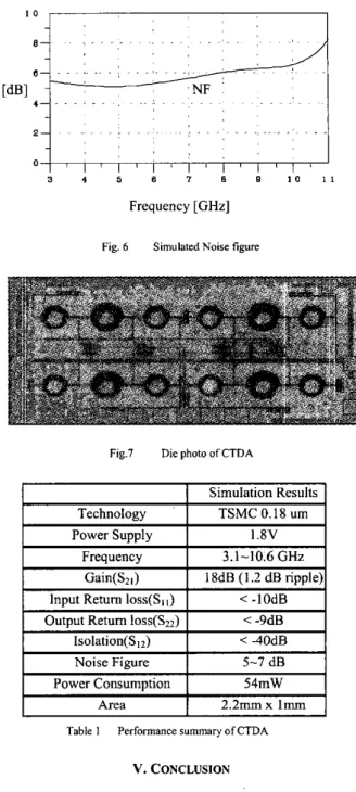
1.8V 3.1-10.6GHz 18dB (1.2 dB ripple) < -IOdB < -9dB < 4 0 d B 5-7 dB 54mW 2.2mm x lmm 3 4 5 6 7 n s i o i i Frequency [GHz]
Fig. 6 SimulatedNoise figurc
The CMOS CTDA was simulated by Advanced Design System (ADS). Fig. 5 and Fig. 6 show the S-parameters and the noise figure of the CTDA. The gain (&I) is 18dB with 1.2dB ripple from 3.1 GHz to 10.6 GHz. The input and output
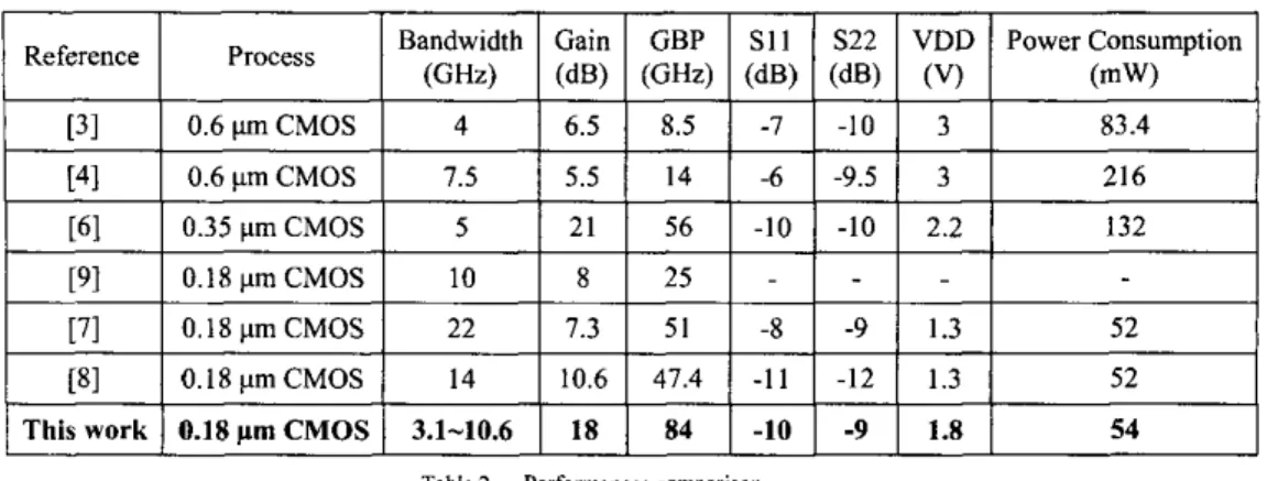
return losses are less than -10dB and -9dB respectively. The reverse isolation S I 2 is 40dB or better over the whole bandwidth. The noise figure is between 5dB and 7dB. Power consumption of the CTDA is only 54mW. Die photo is shown in Fig. 7. Table 1 summarizes the performance of the CTDA. The recently reported performances of CMOS distributed amplifiers compared with this work are summarized in Table 2. This work demonstrates the highest gain-bandwidth production (GBP).
3 0
2 0 ~ 0 0 0 0 0 0 0 0 0 ~ ~ 0 0 ~ ~ ~ ~ ~ 0 0 0 o o o o o o b o o o o o o o o o o
. '. 8 2 , . . . . . ~. .
Fig.7 Die photo of CTDA
I
I
Simulation ResultsTechnoloev '
I
TSMC 0.18 umS A CMOS cascaded two-stage distributed amplifier has been
proposed. The conventional distributed amplifier, CSDA and CTDA have been compared under similar conditions. The CTDA can achieve a voltage gain of 12-24dB using less power consumption than those two. In this work, an 18dB voltage gain CTDA consuming only S4mW has been presented for UWB application. Comparing with other previously published CMOS DAs, this work demonstrates the highest gain-bandwidth production.
. . ,,+!?++++' +;+,+++++++++++ - 5 0 - 8 0
,
I .*: 1 I 3 5 7 8'
, ,
Frequency [GHz]Fig. 5 Simulated S-parameters
2004 IEEE Asia-Pacific Conference on Advanced System Integrated Circuits(AP-ASIC2004)/ Aug. 4-5,2004
Reference Bandwidth Gain GBP S11 S22 VDD PowerConsumption
(GHz) (dB) ( G H 4 (dB) (dB) (V)
(mw)
Process
1
This work 10.18umCMOS1
3.1-10.6I
18I
84I
-10I
-9I
1.81
54I
Table 2 Performances comparison
ACKNOWLEDGEMENT
The authors would like to acknowledge Chien-Chih Lin, Chia-Hsin Wu, Hua-Chin Lee, Chao-Shiun Wang, and Hang- Chie Tsai for technical discussions. This work was supported in part by Media Tek Inc. HsinChu, Taiwan 300.
REFERENCES http:llww.ieee802.org/l Slpub1TG3a.html
P. J. Sullivan, B. A. Xavier, and W. H. Ku, “An Integrated CMOS Distributed Amplifier Utilizing Packaging Inductance,” IEEE Trans. MicrowavcTheoryTech., VOL. 4 5 . p ~ . 1969-1975, Oct. 1997 B. M. Ballweber, R. C u p and D. J. AIIstot, “A Fully Integrated 0.5- 5.5 GHa CMOS Distributed Amplifier,” ISSCC, VOL. 35, NO. 2, FEBRUARY 2000
H. T. Ahn and D. J. Allstof, “A 0.5-8.5 GHz Fully Differential CMOS Distributed Amplifier,’’ ISSCC, VOL. 37, N0.8, AUGUST 2002
B. Ballweber, C. H. Diaq D. Vwk, L. Madden, T. H. Lee, and S. S. Wong, “Monolithic CMOS Distributed Amplifier and Oscillator,” ISSCC Digest ofTech. Papers, 1999, pp. 70-7 I
161 A. Worapirhet, M. Chongcheawchamnan, and S. Strisathit, “Broadband Amplifier in CMOS Technology using Cascade Single- stage Distributed Amplifier,” ELECRONICS LETTERS, VOL. 38, NO. 14,4th N L Y 2002
R. C. Liu; K. L. Deng; H. Wang, “A 0.6-22-GHz Broadband CMOS Distributed Amplifier” IEEE RFIC Symposium, pp.103 - 106, June 8-10,2003
R. C. Liu, C. S. Lin, K. L. Deng, and H. Wang, “A 0.5-14-ghz 10.6- db CMOS Cascode Distributed Amplifier” Digest of Technical Papers. 2003 Symposium on VLSl Circuits, pp.139 - 141, June 12- 14,2003
B. M. Frank, A. P. Freundarfer, Y. M. M. and Antar, “Performance of I-IO-GHz traveling wave amplifiers in 0.l8-Ispl m d m C M O S IEEE Microwave and Wireless Components Letters, VOL. 12, Issue: 9, pp. 327 - 329, Sep 2002
[IO] K. Koumetsov,and A. M. Niknejad, “Design and Analysis of Distributed Amplifier”
[I I] Thomas T. Y. Wong, “Fundamentals of D i s ~ b u t e d Amplifier” 1121 Welborn, XeemeSpecmm, Inc. Project: E E E P802.15 Working
Group for Wireless Personal Area Networks(WPANs) 171
181
191