720 IEEE ELECTRON DEVICE LETTERS, VOL. 34, NO. 6, JUNE 2013
Novel Method for Fabrication of Tri-Gated Poly-Si
Nanowire Field-Effect Transistors With
Sublithographic Channel Dimensions
Ko-Hui Lee, Horng-Chih Lin, Senior Member, IEEE, and Tiao-Yuan Huang, Fellow, IEEE
Abstract— A high-performance short-channel tri-gated polycrystalline-silicon nanowire (NW) field-effect transistor is developed by using simple sidewall spacer and lateral etching techniques without employing costly lithographic tools. Channel length of 120 nm and NW thickness of 25 nm can be easily formed by the self-aligned process. The device exhibits superior electrical characteristics because of the strong gate controllability: a subthreshold swing of 102 mV/dec, drain induced barrier lowing of 74.4 mV/V, and extremely high
ION/IOFF ratio of 4.4× 10⁸(Vd= 1 V) are obtained.
Index Terms— Nanowire, polycrystalline-silicon (poly-Si), self-aligned, short channel.
I. INTRODUCTION
P
OLYCRYSTALLINE-silicon (Poly-Si) nanowire (NW) field-effect transistors (FETs) are promising for the devel-opment of 3-D stackable devices/circuits because of low fab-rication temperatures and mature processes [1], [2]. The NW configuration can further alleviate the severe short-channel effects encountered in the scaling of planar structures because of the enhanced gate controllability [3]. Previously, we pre-sented several innovative top-down approaches for defining the poly-Si NW channels with NW feature size down to 8–20 nm using conventional G-line- or I-line-based lithog-raphy [4]–[6]. However, in those works the channel length (L) of the devices is larger than 400 nm as limited by the capability of the employed lithography technology. For fabricating NW devices with L of around or smaller than 100 nm, deep UV steppers or e-beam writers are usu-ally employed [7], [8]. In this letter, we propose a sim-ple method that combines the sidewall spacer and lateral etching techniques to fabricate tri-gated (TG) poly-Si NW FETs with sublithographic L. Devices of superior performance with L of 120 nm are demonstrated with an I-linebased photolithography.Manuscript received March 16, 2013; accepted March 30, 2013. Date of current version May 20, 2013. This work was supported in part by the Ministry of Education in Taiwan under ATU Program, the NCTU-UCB I-RiCE program under No. NSC-102-2911-I-009-301, and the National Science Council under Contract NSC-99-2221-E-009-167-MY3.
K.-H. Lee and T.-Y. Huang are with the Department of Electronics Engi-neering and Institute of Electronics, National Chiao Tung University, Hsinchu 300, Taiwan.
H.-C. Lin is with the Department of Electronics Engineering and Institute of Electronics, National Chiao Tung University, Hsinchu 300, Taiwan, and also with National Nano Device Laboratories, Hsinchu 300, Taiwan (e-mail: [email protected]).
Color versions of one or more of the figures in this letter are available online at http://ieeexplore.ieee.org.
Digital Object Identifier 10.1109/LED.2013.2256771
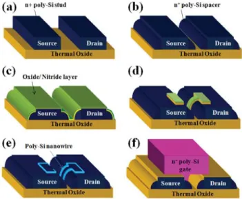
Fig. 1. Stereo views for the main fabrication steps of the short-channel TG-NW FET. (a) Deposition and patterning of an n+poly-Si layer to form the S/D studs. (b) Formation of the n+poly-Si spacers abutting the studs. (c) Deposition of an oxide/nitride stack. (d) Patterning of the oxide/nitride stack. (e) Formation of the poly-Si NW channels. (f) Gate oxide and gate electrode are formed to complete the device.
II. DEVICEFABRICATION
Fig. 1(a)–(f) shows the main fabrication steps for the fabrication of short-channel TG-NW FETs. First, a 180-nm thick n+poly-Si layer is deposited on a thermally oxidized Si wafer. Then a photolithography process with an i-line stepper and an anisotropic dry etching are performed to form two isolated n+poly-Si studs [Fig. 1(a)]. Next, a 150-nm-thick n+ poly-Si layer is deposited and then anisotropically etched to form spacers abutting the n+ poly-Si studs. The two upside-down bowl-shaped n+poly-Si plateaus are used as source and drain (S/D) regions [Fig. 1(b)]. Note that the distance between the S/D determines the channel length, which can be easily shortened to a sublithographic dimension with the formation of poly-Si spacers. The subsequent steps [Fig. 1(c) and (d)] are employed for the formation of the twin NW channels and the flow, as further shown in Fig. 2(a)–(d), is similar to that presented in our previous paper [6]. In the figures, the illustrations are the cross-sectional structures perpendicular to the source-to-drain direction formed after each individual step. Tetraethoxysilane (TEOS) oxide (30 nm)/nitride (30 nm) (O/N) stacked layers are deposited sequentially [Fig. 1(c)]. A dummy structure connecting S/D regions is then patterned [Figs. 1(d) and 2(a)]. A diluted HF solution is subsequently
LEE et al.: NOVEL METHOD FOR FABRICATION OF TRIGATED POLY-Si NANOWIRE FIELD-EFFECT TRANSISTORS 721
Fig. 2. Detailed lateral etching processes for the formation of the twin NW channels. (a) Anisotropic etching of the oxide/nitride stack. (b) Selective etching of the TEOS oxide with HF. (c) Deposition of a poly-Si layer, following by an anisotropic etching to define the NW channels. (d) Removal of the TEOS oxide/nitride stack.
(a) (b)
(c)
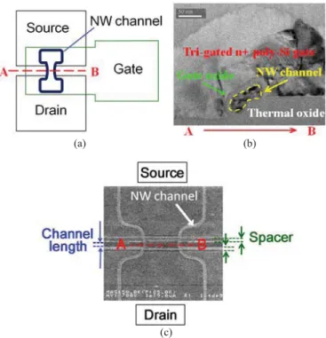
Fig. 3. (a) Layout of the TG-NW FET. (b) Cross-sectional TEM image of a fabricated device along A-B line in (a). (c) Top view SEM image of the device taken before the formation of the gate electrode. The channel length (L) is determined to be 120 nm.
used to etch the TEOS oxide laterally to create undercuts beneath the nitride [Fig. 2(b)]. Then an amorphous silicon (α-Si) layer is deposited to refill the undercuts [Fig. 2(c)], followed by a solid phase crystallization process (SPC at 600 °C in N2ambient for 24 h). Twin NW channels are defined
by dry etching with the top nitride as hard mask. The O/N dummy structure is then removed by wet etching, as shown in Figs. 1(e) and 2(d). Finally, gate oxide (12 nm) and n+poly-Si electrode are formed to complete the device [Fig. 1(f)].
III. RESULTS ANDDISCUSSION
Fig. 3(a) shows the schematic top view of the device. Transmission electron microscopy and scanning electron
Gate Voltage (V) -0.5 0.0 0.5 1.0 1.5 2.0 Drai n Cu rrent (A/ µ m) 10-13 10-12 10-11 10-10 10-9 10-8 10-7 10-6 10-5 10-4 Vd = 0.1 V Vd= 1 V S.S. = 102 mV/dec (@ Vd= 0.1 V) DIBL = 74.4 mV/V (@ Id= 1 x 10⁻⁸ V) Vth = - 0.17 V (@ Id= 1 x 10 -8 V) ION/IOFF = 4.4 x 10 8 (@ V d= 1 V, Vg= 4 V)
Fig. 4. Transfer characteristics of a fabricated TG-NW FET with L = 120 nm. 0 1 2 3 0 20 40 60 80 100 120 TG-NW FET Drai n Cur rent ( µ A/ µ m) Drain Voltage (V) Vg-Vth = 0 ~ 3 V , Step = 0.5 V
Fig. 5. Output characteristics of the fabricated TG-NW FET.
microscopy (SEM) are employed to check the completed device structure and the preliminary results are shown in Fig. 3(b) and (c), respectively. Fig. 3(b) shows the cross-sectional images of one of the formed NW channels along the A-B direction shown in Fig. 3(a). The NW thickness
is ∼ 25 nm and the gated width of the fin is ∼ 120 nm.
Fig. 3(c) shows the top-down SEM image of the TG-NW FET, and L is determined to be 120 nm, about a third of the resolution capability (∼ 350 nm) of the i-line stepper.
Transfer characteristics of a fabricated TG-NW FET (L = 120 nm and effective width(W) = 240 nm (two NW channels) are shown in Fig. 4. The threshold voltage (Vth), defined as
the VG when the drain current reaches (W/L) × 10 nA at
Vd = 0.1 V, is −0.17 V. Superior device performance with
high ION/IOFF ratio (> 108), good S.S. (102 mV/dec) and low drain induced barrier lowing (DIBL) (74.4 mV/V) is recorded in the figure. Fig. 5 shows the output characteristics of the TG-NW FET. The driving current at Vg–Vth = 3 V and
Vd = 1 V reaches 40 μA/μm. Device characteristics are
expected to improve with additional plasma treatment [7]. We compare the extracted parameters of the TG-NW FET with state-of-the-art NW devices in Table I [8]–[11]. The tiny body of NW channels reduces the leakage path and suppresses the leakage current. Therefore, in Table I, our work shows an extremely high ION/IOFFratio. Also, the strong
722 IEEE ELECTRON DEVICE LETTERS, VOL. 34, NO. 6, JUNE 2013
TABLE I
COMPARISON OFKEYDEVICEPARAMETERS OFNW-CHANNEL FETS INTHISLETTER ANDOTHERSTUDIES
This
Paper Ref. [8] Ref. [9] Ref. [10] Ref. [11] Type
Tri-gated
Tri-gated DG GAA GAA
Lithography Method i-line
e-beam
+ DUV i-line e-beam e-beam
Crystallization SPC NA SPC SPC NA
NH3plasma W/O W/O W/O W W/O
W/L (nm/nm) 240 /120 45 /100 300 /1000 90 /30 90 /100 T(SiO2)(nm) 12 1.7 20 25 4.5 S.S. (V/dec) 0.102 0.087 0.073 0.224 0.1 DIBL(V/V) 0.074 0.078 0.012 0.895 0.060 Ion/Ioff (Vd¡F Ion@Vg) > 108 Vd=1 V Vg=2 V > 104 Vd=1 V Vg=1 V > 106 Vd=0.5 V Vg=3 V > 107 Vd=1 V Vg=4 V > 107 Vd=1.2 V Vg=2 V
gate controllability effectively enhances the S.S. of the device. Noteworthy in the table is the use of the mature I-line-based technique demonstrated in our paper for the fabrication of small-scale devices with throughput greatly surpassing that of e-beam writers and overall process cost significantly lower than that using DUV steppers. With further refinement in process conditions, fabrication of devices with L down to 100 nm or less would be feasible using the proposed method. In addition, the operation voltage could be lowered as the equivalent oxide thickness of the gate dielectric is further thinned down.
IV. CONCLUSION
In this letter, a novel scheme for fabricating TG poly-Si NW FET with sublithographic L was proposed and demonstrated. This scheme adopted sidewall-spacer etching to shorten L and lateral etching to define the NW channels. With an I-line-based lithography, a fabricated device with L of 120 nm and NW thickness of 25 nm showed excellent electrical performance in terms of good S.S., small DIBL, and high ION/IOFF ratio. This flexible approach was feasible for fabricating test devices
for probing the nanoscale phenomena and manufacturing of future 3-D stackable devices/circuits.
REFERENCES
[1] Y. Fukuzumi, R. Katsumata, M. Kito, M. Kido, M. Sato, H. Tanaka, Y. Nagata, Y. Matsuoka, Y. Iwata, H. Aochi, and A. Nitayama, “Optimal integration and characteristics of vertical array devices for ultra-high density, bit-cost scalable Flash mem-ory,” in Proc. IEEE Int. Electron Devices Meeting , Dec. 2007, pp. 449–452.
[2] N. Singh, A. Agarwal, L. K. Bera, T. Y. Liow, R. Yang, S. C. Rustagi, C. H. Tung, R. Kumar, G. Q. Lo, N. Balasub-ramanian, and D. L. Kwong, “High-performance fully depleted silicon nanowire (diameter ≤ 5 nm) gate-all-around CMOS devices,” IEEE Electron Device Lett., vol. 27, no. 5, pp. 383–386, May 2006.
[3] H. C. Lin, M. H. Lee, C. J. Su, and S. W. Shen, “Fabrication and char-acterization of nanowire transistors with solid-phase crystallized poly-Si channels,” IEEE Trans. Electron Devices, vol. 53, no. 10, pp. 2471–2477, Oct. 2006.
[4] H. C. Lin, M. H. Lee, C. J. Su, T. Y. Huang, C. C. Lee, and Y. S. Yang, “A simple and low-cost method to fabrication TFTs with poly-Si nanowire channel,” IEEE Electron Device Lett., vol. 26, no. 9, pp. 643–645, Sep. 2005.
[5] H. C. Lin and C. J. Su, “High-performance poly-Si nanowire NMOS transistors,” IEEE Trans. Nanotechnol., vol. 6, no. 2, pp. 206–212, Mar. 2007.
[6] H. H. Hsu, T. W. Liu, L. Chan, C. D. Lin, T. Y. Huang, and H. C. Lin, “Fabrication and characterization of multiple-gated poly-Si nanowire thin-film transistors and impacts of multiple-gate structures on device fluctuations,” IEEE Trans. Electron Devices, vol. 55, no. 11, pp. 3063–3069, Nov. 2008.
[7] C. M. Lee and B. Y. Tsui, “High-performance poly-Si nanowire thin-film transistors using the HfO2 gate dielectric,” IEEE Electron Device
Lett., vol. 32, no. 3, pp. 327–329, Apr. 2011.
[8] M. Im, J.-W. Han, H. Lee, L.-E. Yu, S. Kim, S. C. Jeon, K. H. Kim, G. S. Lee, J. S. Oh, Y. C. Park, H. M. Lee, and Y.-K. Choi, “Multiple-gate CMOS thin-film transistor with polysilicon nanowire,” IEEE Electron Device Lett., vol. 29, no. 1, pp. 102–105, Jan. 2008.
[9] W. C. Chen, H. C. Lin, Y. C. Chang, D. C. Lin, and T. Y. Huang, “In situ doped source/drain for performance enhancement of double-gated poly-Si nanowire transistors,” IEEE Trans. Electron Devices, vol. 57, no. 7, pp. 1608–1615, Jul. 2010.
[10] C. M. Lee and B. Y. Tsui, “A high-performance 30-nm gate-all-around poly-Si nanowire thin-film transistor with NH3plasma treatment,” IEEE
Electron Device Lett., vol. 31, no. 7, pp. 683–685, Jul. 2010.
[11] T. T. Le, H. Y. Yu, Y. Sun, N. Singh, X. Zhou, N. Shen, G. Q. Lo, and D. L. Kwong, “High-performance poly-Si ver-tical nanowire thin-film transistor and the inverter demonstra-tion,” IEEE Electron Device Lett., vol. 32, no. 6, pp. 770–772, Jun. 2011.