國 立 交 通 大 學
電子工程學系 電子研究所碩士班
碩 士 論 文
利用雙重微影成像法製作 P 型金氧半場效電晶體
之元件特性和可靠度研究
A Study on the Fabrication, Characterization,
and Reliability Issues of PMOSFETs with
Double-Patterning Technique
研 究 生:卞孝雄
指導教授:林鴻志 博士
黃調元 博士
利用雙重微影成像法製作 P 型金氧半場效電晶體
之元件特性和可靠度研究
A Study on the Fabrication, Characterization,
and Reliability Issues of PMOSFETs with
Double-Patterning Technique
研 究 生:卞孝雄
Student:Siao-Syong Bian
指導教授:林鴻志 博士 Advisors:Dr. Horng-Chih Lin
黃調元 博士
Dr. Tiao-Yuan Huang
國 立 交 通 大 學
電子工程學系 電子研究所碩士班
碩 士 論 文
A Thesis
Submitted to Department of Electronics Engineering & Institute of Electronics College of Electrical and Computer Engineering
National Chiao-Tung University in Partial Fulfillment of the Requirements
for the Degree of Master of Science
in
Electronic Engineering August 2011
Hsinchu, Taiwan, Republic of China
利用雙重微影成像法製作 P 型金氧半場效電晶體
之元件特性和可靠度研究
研究生 : 卞孝雄 指導教授 : 林鴻志 博士
黃調元 博士
國立交通大學
電子工程學系 電子研究所碩士班
摘要
在本篇論文中,我們利用先前所開發的一種雙重微影成像技術,以 I 射線光學 步進機,成功製作出 80 奈米閘極線寬的 P 型金氧半場效電晶體。這方法使用了兩 個不同光罩,藉由兩次微影和蝕刻製程來形成閘極圖形。雖然製程步驟較傳統標 準作法複雜,但是可以打破傳統 I 射線光學解析度的限制,並且能夠實現非對稱元 件的製作。我們藉由電腦輔助軟體模擬,可以檢視非對稱延伸區的摻雜分佈來形 成超淺接面。在本篇論文中,我們使用並分析不同閘極堆疊模組對於元件特性上 的影響,包含硼穿透和可靠度問題,也使用不同方式形成超淺接面。 我們發現,由於氧增強硼擴散效應的作用,屏蔽氧化層無助於形成超淺接面。 而利用大分子化合物離子像 BF2+和低能量佈植,並且改善後續熱退火處理是可改 善超淺接面製作的方法。事實上,氟會增加硼穿透能力,而且造成較大的閘極空乏區,減少驅動電流能力。然而在可靠度方面,氟的摻入是對減少負偏壓溫度不 穩定性有益的。最後,我們比較負偏壓溫度不穩定模式和通道熱載子模式下造成 的變化差異,負偏壓不穩定性的影響是較為嚴重而且必須加以重視的。
A Study on the
Fabrication, Characterization,
and Reliability Issues of PMOSFETs with
Double-Patterning Technique
Student : Siao-Syong Bian Advisors : Dr. Horng-Chih Lin
Dr. Tiao-Yuan Huang
Department of Electronics Engineering and Institute of Electronics
National Chiao Tung University, Hsinchu, Taiwan
Abstract
In this thesis, we have employed a double-patterning technique previously developed by our group to fabricate PMOSFETs with gate length down to 80 nm using only a conventional I-line stepper. The DP method takes advantages of two distinct masks which are used in the litho-etch-litho-etch (LELE) process to form the gate patterns. Although more process steps are needed than conventional single patterning method, LELE process breaks the resolution limit of conventional I-line lithography and enables the feasibility of asymmetric MOSFETs. With the aid of technology computer-aided design (TCAD) simulation, the doping profiles of asymmetric ultra shallow extensions are designed. In this work, we have also investigated and analyzed the effects of gate stack modules on the device characteristics, including boron penetration and reliability issues.
We have found that the screen oxide prevalently used for suppressing channeling effect may have negative impact on the formation of ultra-shallow junctions owing to the occurrence of oxygen enhanced diffusion (OED). Use of molecular ion species such as BF2+, lowering the implant energy, and carefully adjusting the
post-implant annealing conditions are feasible to achieve ultra shallow junction. Fluorine incorporation is advantageous of reducing NBTI effect in short channel devices. However, as fluorine is involved, enhanced boron penetration and poly gate depletion that reduces the drive current are potential issues that should be concerned. We’ve also assessed the NBTI and CHI reliability characteristics of the fabricated devices. The results indicate that the NBTI effect is more serious than the latter.
Acknowledgement
我的人生是個美麗的方波,渡過當兵艱辛的歲月,重拾書本再考研究所, 指顧間 2 年碩士生涯過去,跨過重重障礙,終於達成自己的夢想。在這裡要特別 感謝兩位指導教授林鴻志博士和黃調元博士。林鴻志老師讓我學習到正確分析元 件想法和積極的實驗態度,將實驗中所學和課本上知識做連結與驗證,黃調元老 師的學術上的風範以及當黃老師記憶體元件課程的助教,都讓我有許多不同思考 方向和啟發。 在這裡真的要非常謝謝國家奈米實驗室的吳志明研究員,給予我實驗上的幫 助,再來要感謝的是 ADTL 的學長們,蔡子儀學長在 NDL 的經驗和功力,使得我 的實驗事半功倍,不虧是 NDL 的扛壩子。林哲民學長在元件模擬和理論上也分享 給我許多寶貴經驗。也不能忘記感謝林政頤學長在實驗和量測上的幫助,在我第 一批貨失敗時給我鼓勵,以及蘇俊榮博士、郭家豪學長、徐行徽博士、陳威臣博 士,你們總是樂於回答我的問題。另外特別感謝前一屆學長簡敏峰,在你的帶領 下,我很高興可以加入博大精深的 MOS 家族。碩士求學中的同學們:王崇名、蘇 段凱、林歷樺、鍾嘉文、吳俊鵬、顏同偉、許宇賢,兩年多和你們相處真的是很 有趣,也祝歷樺和鍾大師博班之路順利。 也感謝之前的同學和學長支持,湘彥、建民、老爹、京霖、益洵和俊瑋,謝 謝你們不定期在 MSN 和 Facebook 上噓寒問暖使我能度過火盃的考驗,拿到死神 的聖物-畢業證書。最後要感謝的是我的母親和妹妹,你們默默關心和支持,是 我完成這一份論文不可或缺的神秘力量。謝謝所有曾經幫助過我的人,衷心感謝, 期待再相逢。 卞 孝 雄 誌於風城交大 2011 年 8 月Contents
Abstract (Chinese)………... i
Abstract (English)………... iii
Acknowledgement (Chinese)……….. v
Contents ………... vi
Figure Captions………... viii
Table Captions ……….... xiii
Chapter 1 Introduction………...
11.1 General Background…...………. 1
1.1.1 Introduction……….. 1
1.1.2 Lithography and Double Patterning Technique…….………... 2
1.2 Silicon Gate Technology and Boron Penetration………... 4
1.3 Ultra-Shallow Junction MOSFETs……….. 5
1.4 Motivation………... 6
1.5 Organization of the Thesis ………. 6
Chapter 2 Device Fabrication and Measurement Setup………..
82.1 Double Patterning Technique ………. 8
2.2 TCAD Simulation and Device Fabrication………..………... 9
2.2.1 TCAD Simulation for Asymmetric S/D Extensions………..…….. 9
2.3 Measurement Setup…. ………... 12
2.3.1 Electrical Measurement Setup……….. 12
2.3.2 NBTI and CHC Reliability Measurement Setup……….…. 12
2.3.3 Charge Pumping Measurement……… 13
Chapter 3 Results and Discussion ……… 16
3.1 Electrical Characteristics of Symmetric-Extension Devices….……….. 16
3.1.1 Boron Penetration with Poly-Si Gate………... 16
3.1.2 Accomplishment of 80nm Devices without Boron Penetration…………... 17
3.2 Electrical Characteristics of Asymmetric-Extension Device………... 20
3.3 NBTI and CHC Degradations on PMOSFETs……… 22
3.3.1 Background………... 22
3.3.2 Channel Length and Gate Stack Dependences on NBTI…………... 24
3.3.3 Comparisons between CHC and NBTI Stresses……….. 25
Chapter 4 Conclusion and Future Work………... 28
4.1 Recapitulation and Conclusion……….…………... 4.2 Future Work………... 28 30 References ………... Figures………... 31 38 Vita……… 66 Publication List……… 67
Figure Captions
Chapter 1
Fig. 1.1. Historical trends of physical gate length of microprocessor unit (MPU) versus year [2]. ……….. 38
Chapter 2
Fig. 2.1. Design of the double patterning masks. Overlap region of G1 and G2 masks in the active region is the nominal gate length. …... 39 Fig. 2.2.
In-line SEM images and measured gate lengths for poly-Si patterns in the selected dies with nominal gate length of 100nm. ……… 39 Fig. 2.3. In-line SEM images and measured gate lengths for poly-Si patterns with
nominal gate length of 80nm. The test structures were selected from dies characterized in Fig. 2.2. ………... 40 Fig. 2.4. In-line SEM images and measured gate lengths for poly-Si patterns with
nominal gate length of 60nm. The test structures were selected from dies characterized in Fig. 2.2. The measured dimension is much smaller than Lmask, indicating the CD is out of control at such a small
dimension. ………... 40 Fig. 2.4. In-line SEM images and measured gate lengths for poly-Si patterns with
nominal gate length of 60nm. The test structures were selected from dies characterized in Fig. 2.2. The measured dimension is much smaller than Lmask, indicating the CD is out of control at such a small dimension. …….. 41
Fig. 2.5. In-line SEM images for poly-Si patterns measured in four different dies with nominal gate length of 80nm. The measured gate lengths show good CD control even for the corner dies. ………. 41 Fig. 2.6. Due to the use of source-side screen oxide, junctions formed by B+ and
BF2+ have similar junction profile. ……… 42
Fig. 2.7. The activated carrier concentration of the As-doped regions implies that halo implantation participated in the S/D junction construction. ………….. 42 Fig. 2.8. The highlight of lateral doping profile along the channel shows no
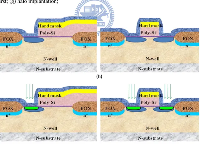
significant discrepancy between S and D extensions. ………... 43 Fig. 2.9. Illustration of device fabrication flow:
(a) LOCOS isolation; (b) gate oxide and poly deposition; (c) gate implantation; (d) hard mask deposition; ………. 43 Fig. 2.10. (cont.) (e) G1 mask definition; (f) symmetric devices defined by G2 mask
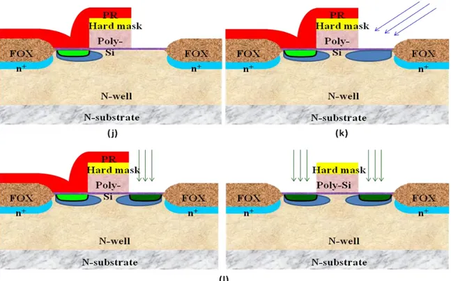
first; (g) halo implantation; ………... 44 Fig. 2.11. (cont.) (h) capping screened oxide; (i) source side extension of asymmetric
devices and the split A of symmetric devices formed by B+; ……… 44 Fig. 2.12. (cont.) (j) asymmetric devices defined by G2 mask; (k) halo implantation;
(l) drain side extension of asymmetric devices and the split B of symmetric devices formed by BF2+; ……… 45
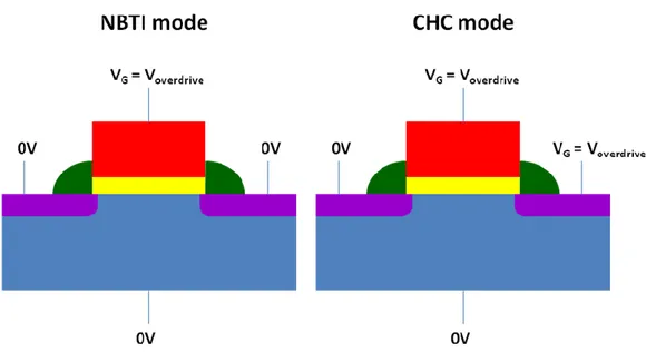
Fig. 2.13. (cont.) (m) sidewall spacer formation; (n) deep S/D implantation; (o) TEOS passivation; (p) metal contact definition and forming gas annealing. ………... 45 Fig. 2.14. Schematics showing the measurement biases for the NBTI mode and CHC
mode. ………. 46
Fig. 2.15. Fundamental setup structure for charge pumping measurements. ………… 46 Fig. 2.16. Lateral charge pumping measurement setup for detached side of single
junction. For example, the lateral distribution of generated interface states after stress was extracted near the drain side. ……… 47 Fig. 2.17. Schematic illustrations for the charge pumping measurement of different
pulse conditions: (a) fixed amplitude; (b) fixed peak sweep; (c) fixed base sweep. ……….... 47
Chapter 3
Fig. 3.1. Transfer characteristics of devices with channel length of 10 μm and B-doped gate fabricated with double patterning or single patterning scheme. ………... 48 Fig. 3.2. Transfer characteristics of devices with channel length of 10 μm and
BF2-doped gate fabricated with double patterning or single patterning
scheme. Gate leakage current is high, presumably because of fluorine incorporation. ………. 48 Fig. 3.3. Transfer characteristics of devices with B-doped gate for channel length of
0.2 μm and 0.12 μm. ……….. 49 Fig. 3.4. Transfer characteristics of devices with BF2 -doped gate for channel length
of 0.2 μm and 0.12 μm. ……….. 49 Fig. 3.5. (a) Schematic showing boron diffusion from the heavily doped P+ ploy
gate into gate oxide and interface region for conventional SiO2 and (b)
interaction of the boron with the nitrogen piled-up at the channel/oxide interface [38]. ………. 50 Fig. 3.6. Transfer characteristics of B- and BF2-doped devices with channel length
of 10 μm. The solid lines are for VDS = -0.05V and dash lines for VDS =
-1V. ………. 51 Fig. 3.7. Transfer characteristics of devices with B-doped gate and various channel
length of 1 μm and 0.08 μm. ……….. 51 Fig. 3.8. Transfer characteristics of devices with BF2-doped gate and various
channel length of 1 μm and 0.08 μm. ……… 52 Fig. 3.9. Output characteristics of devices with B-doped gate and channel length of
0.08 μm. ………... 52 Fig. 3.10. Output characteristics of devices with BF2-doped gate and channel length
of 0.08 μm. ………. 53 Fig. 3.11. Threshold voltage as a function of gate length for devices with BF2- and
B-doped gates. ……… 53 Fig. 3.12. DIBL as a function of gate length for devices with BF2- or B-doped gate. ... 54
Fig. 3.13. SS as a function of gate length for devices with BF2- or B-doped gate. …… 54
Fig. 3.14. Ion as a function of gate length ranging from 0.08 to 10 μm for devices with BF2- or B-doped gate. ……… 55
Fig. 3.15. Comparisons of transfer characteristics of an NMOSFET with PMOSFETs with BF2- or B-doped gate. The devices are with an identical channel
length of 0.1μm. The solid symbols are for VDS = -0.05V and hollow
symbols for VDS = -1V. ……….. 55
Fig. 3.16. C-V curves of devices with B- or BF2-doped gate. Results for devices
exhibiting B-penetration effects are also shown. The measurement frequency is 100 kHz. ……… 56 Fig. 3.17. A sketch of the asymmetrical PMOSFETs and configuration of forward
Fig. 3.18. Transfer characteristics of the asymmetric device with channel length of 10 μm. ………... 57 Fig. 3.19. Output characteristics of the asymmetric device with channel length of 10
μm. ………. 57 Fig. 3.20. Transfer characteristics of the single-patterning device with symmetric
extension by B implantation. It suggests that leakage current is not incurred by the DP technique. ……….. 58 Fig. 3.21. Transfer characteristics of the asymmetric device with channel length of
0.2 μm. ………... 58 Fig. 3.22. Output characteristics of the asymmetric device with channel length of 0.2
μm. ………. 59 Fig. 3.23. Threshold voltage as a function of gate length for devices with different
extension. ………... 59 Fig. 3.24. Transfer characteristics of the asymmetric device under forward mode.
Drain voltage increases from -0.1V to -1V by step of -0.1V. ……… 60 Fig. 3.25. Transfer characteristics of the asymmetric device under forward mode
measured at different temperature. ……… 60 Fig. 3.26. Threshold voltage shift versus stress time for B-gate devices of different
channel lengths at various temperatures under NBTI mode. ………. 61 Fig. 3.27. Threshold voltage shift versus stress time for BF2-gate devices of different
channel lengths and at various temperatures under NBTI mode. ………….. 61 Fig. 3.28. Comparisons of NBTI results at 125℃ among devices with different
channel lengths and/or various gate stack modules. ……….. 62 Fig. 3.29. Fixed amplitude charge pumping curves of a B-gate device with channel
length of 10μm before and after NBTI stress. ………... 62 Fig. 3.30. Fixed amplitude charge pumping curves of a B-gate device with channel
length of 0.1μm before and after NBTI stress. ……….. 63 Fig. 3.31. Normal and reverse lateral charge pumping curves of a B-gate device with
channel length of 0.1μm before and after NBTI stress. ………. 63 Fig. 3.32. A sketch of the symmetric PMOSFETs and configuration of forward and
reverse modes of operation. ………... 64 Fig. 3.33. Threshold voltage shift versus stress time under NBTI or CHC stress at
forward and reverse measurement modes. ………. 64 Fig. 3.34. Fixed amplitude charge pumping curves of a B-gate device with channel
length of 0.1μm before and after CHC stress. ………... 65 Fig. 3.35. Normal and reverse lateral charge pumping curves of the B-gate device
Table Captions
Chapter 2
Table 2.1. Process conditions for TCAD simulation. ………... 15 Table 2.2. Split conditions for extension structure with the DP technique. ………….. 15
Chapter 3
Table 3.1. Capacitance equivalent thicknesses of devices with B- or BF2-doped gates. Devices with serious boron penetration are also included. ………... 27 Table 3.2. Estimated poly-depletion thickness from the difference in CETs measured
in accumulation and inversion regions. ………... 27
Chapter 1
Introduction
1.1 General Background
1.1.1 Introduction
Since the early 1970’s, evolution of the semiconductor manufacturing technology has followed the Moore’s law for scaling of transistors. In 1965, Dr. Moore stated that the number of transistors integrated in a chip doubled every two years [1]. Although the period for two times increase in transistor number in practical development is not exactly two years, Moore’s law is still a virtuous cycle which in turn allows further investments in semiconductor manufacturing and further scaling in device’s dimensions. By means of transistor scaling, integrated circuits (IC) would obtain a better performance, which gives rise to a great deal of growth of the semiconductor market. Because of plentiful profitability, semiconductor manufacturing companies could invest in equipment for shrinking progresses. Figure 1.1 shows the historical trends of the physical gate length for the microprocessor unit (MPU) in the past decades [2] and 22nm MPU has been demonstrated by Intel [3].
To achieve higher performance and density, CMOS devices have been scaled into nanometer scale, although many issues obstructing the progress are encountered. For examples, the major limiting factors for MOSFET are the well-known short-channel effects (SCEs), including threshold voltage (Vth) roll-off with
decreasing gate length (Lg) and drain-induced barrier lowing (DIBL). Accompanying
with the reduction in operation voltage, the reduction in Vth leads to a significant
increase in the off-state current(Ioff), which results in more power consumption [4].
2
junction capacitances degrade the CMOS delay [5]. Furthermore, both avalanche breakdown and punch-through would occur in short-channel devices, if the device not properly scaled [6]. More new problems would emerge in the development of the next generation technology. It demands the semiconductor industry to develop substantial and advanced techniques to overcome these dilemmas for continuing and extending the Moore’s law.
On the other hand, reliability issues arising from device operation and surrounding environment are always challenging. Operation voltage and temperature effects are important factors that affect device reliability. In recent years, negative bias temperature instability (NBTI) for PMOS and channel hot-carrier (CHC) effects have received much attention. In other words, both of them bring about reduction of the IC lifetime. However, the physical mechanisms are still not very clear and it is difficult to find out an efficient detection solution [7].
1.1.2 Lithography and Double Patterning Technique
Lithography is arguably the most important technique in IC fabrication for shrinking the size of the devices. In general the capability of a lithographic process is related to its resolution R which follows the Rayleigh criterion [8]:
R K NA 1 , (1.1)
where λ is the wavelength of the light, NA is the numerical aperture, and K1 is a
system constant. The resolution signifies the minimum printable half-pitch dimension that could be accomplished. Traditionally we could obtain a higher resolution by means of reduction of wavelength. For instance, the light source of exposure tools has been converted from G-line (436nm), I-line (365nm), KrF excimer laser (248nm), to ArF excimer laser (193nm). It is evident that decreasing wavelength is not the only
way to delineate finer patterns. Using lens with a larger NA to capture higher order of diffracted lights is another way to achieve higher solution, but there is a tradeoff between resolution and depth-of-focus (DOF) which has the following form:
NA K DOF 2 2
, (1.2) where K2 is a system constant. A reduction in DOF would cause more difficulty infabrication, however. In fact, resolution enhancement techniques such as off-axis illumination (OAI), phase shift mask (PSM), optical proximity correction (OPC), and immersion lithography have also been adopted to reduce K1. In spite of the great
accomplishments mentioned before, development of the next-generation lithography (NGL) beyond 32nm has been nebular so far. The options for NGL include extreme ultra-violet (EUV), electron beam lithography, and double patterning (DP) method. Cost of EUV systems and process are expected to be extremely high and the manufacturing technique is actually not ready due to a lack of intensive and stable power sources, defect-free masks, and issues related to resists and metrology infrastructure [9]. Electron beam lithography suffers from a low throughput and is not suitable for mass production [10]. Therefore, DP has emerged as a potential way for NGL because it can be realized with currently available exposure tools [11-12].
Since excimer laser tools are quite expensive [13], they are hardly affordable for the academic organizations. As a result, electron beam lithography is usually adopted in academic laboratories to generate nano-scale patterns, although the fabrication throughput is seriously limited. In our previous work [14], we’ve developed a DP method by utilizing an I-line stepper to fabricate MOSFETs with deep-submicron or even sub-100 nm channel length, and have successfully demonstrated the feasibility of achieving elevated resolution, while maintaining considerable throughput as well.
4
1.2 Silicon Gate Technology and Boron Penetration
The scaling of CMOS is driven by the requirements of improved speed and low power operation. Introduction of self-aligned process, in which the S/D diffusion layer is formed by using gate electrode as a mask of implantation, in mid-1970s makes aggressive scaling possible [14]. By using thermally stable silicon for gate electrodes, S/D can be formed after the gate formation. The key for low power operation is the lowering of drain voltage Vdd and Vth. To lower the Vth of transistors,
work functions of gate electrodes are individually optimized for n-MOSFET and p-MOSFET in deep sub-micron nodes and beyond. Dual-doped polysilicon process provides the low and symmetric Vth which are indispensable for low Vdd operation
[15]. Moreover, since both NMOS and PMOS devices have surface-channel conduction in the dual poly scheme by virtue of dual-doped polysilicon gates, the SCEs are reduced while the subthreshold characteristics are improved [16].
The major challenge for dual-doped gate stack is diffusion of boron from heavily-doped p+-polysilicon through the thin gate oxide and into the channel region during subsequent dopant activation and annealing steps [17]. This phenomenon, the so-called boron penetration, results in Vth shift, subthreshold slope degradation,
degraded low field mobility, increased charge trapping rate, and reduced process margin [18]. On the other hand, insufficient dopant activation inflicts on gate depletion and degrades driving current [19]. Hence, the thermal budget of a dual-poly CMOS process must be carefully designed to take boron penetration and gate depletion into consideration [20].
Boron penetration can be inhibited by using thermally nitrided oxide grown in N2O ambient as a diffusion barrier. These N2O grown gate dielectrics are widely
reliability [21]. Accordingly, in this thesis we adopt N2O grown dielectric as the gate
insulator for ultra thin oxide MOSFETs.
1.3 Ultra-Shallow Junction MOSFETs
Since MOSFET gate dimensions have been dramatically reduced from 10μ m to below 100 nm through a combination of aggressive gate oxide thickness and junction depth scaling [22]. The aggressive scaling aims at suppressing the SCEs mentioned previously. Vth roll-off comes from charge sharing with S/D depletion, and halo
implantation is an effective technique against Vth roll-off, by reducing the depletion
width in S/D junctions. Moreover, DIBL occurs in short-channel devices when the drain depletion width becomes comparable to the channel length, causing the lowering of source barrier height and the injection of extra minority carriers. Its conduction is through the channel surface so the subthreshold swing (SS) is not affected. In the case of higher drain bias, source and drain depletion regions in the bulk are connected and SS is dramatically degraded. For the purpose of shrinking S/D depletion, ultra shallow junction plays an important role in achieving SCE immunity [23].
Ultra shallow junctions can be realized by utilizing techniques like low energy implant [24], plasma doping [25], spike annealing [26], and raised S/D [27]. With their decent throughput and good reproducibility, low energy implant and spike annealing are adopted as the de facto standard process for nano-scale devices. Since a boron ion has a rather light effective mass, it has a big projected range and exhibits the channeling effect. Thus p+-n ultra shallow junction represents a specific challenge for PMOSFETs [28]. Implanting molecular species such as BF2+, modifying implanter
for low energy operation, and improving the post-implant annealing are main efforts to achieve ultra shallow junction with low resistance and abrupt doping profile. In fact,
6
ultra shallow junction still has a lot of concerns including transient-enhanced diffusion (TED), oxygen-enhanced diffusion (OED), dopant activation, defect elimination, and junction leakage.
1.4 Motivation
It has been reported that flourine enhances the diffusion of boron in N2O grown
oxides and flourine diffuses through the polysilicon when BF2 implant is used in
polysilicon gate. Although BF2 enhances boron penetration, it is indeed an excellent
approach to form USJ. In addition, some recent reports discovered that BF2+
implantation results in anomalous NBTI effect in short channel devices [29]. In this work, we fabricate the deep-submicron and nano-scale devices by a DP technique, accompanying by different boron and BF2+ implantation in gate and S/D extensions.
In this way, we can examine and comprehend the role of flourine through the analysis made on short-channel devices.
1.5 Organization of the Thesis
In Chapter 1, we introduce the evolution of lithography and device technology.
In Chapter 2, we present the fabrication of PMOSFETs with channel length
down to 80 nm and describe the process flow utilizing the DP technique. TCAD simulation and measurement setups are also presented in this chapter.
In Chapter 3, electrical characteristics of the fabricated devices with various annealing temperature are presented. Both transfer curves and capacitance-voltage (C-V) characteristics are analyzed to indentify boron penetration and gate depletion. For the sake of reliability issues, NBTI and CHC stress are undergone and charge pumping measurements are taken place for understanding the degradation of MOS
transistors.
Eventually, in Chapter 4, we summarize the major conclusions based on the analysis of our experimental results.
8
Chapter 2
Device Fabrication and Measurement Setup
2.1 Double Patterning Technique
In this section, we present a double patterning (DP) technique which combines
twice lithographic and subsequent etching steps using an I-line stepper to fabricate and demonstrate 80nm p-channel MOSFETs. The intended design patterns are defined by virtue of two distinct masks which are denoted as G1 and G2 and shown in Fig. 2.1. The masks are used in the litho-etch-litho-etch (LELE) process [30] to form the final device’s gate structure. In the first place, we utilize the G1 mask to shelter poly-Si on the right side of active region from the first etching step, whereas the uncovered Si region is established as the source region. Next, the task of G2 mask is to prevent the left side of active region from succeeding etching process for the sake of drain side definition, including a fraction of poly-Si region remained after the first etching. The overlapped region between the G1 and G2 masks defines the gate length, which is the most critical metric of the pattern size. No doubt LELE process is obliged to add an additional mask, raising process complexity. However, LELE process breaks the resolution limit of conventional I-line lithography and enables the feasibility of asymmetric MOSFETs [31].
The above DP process was carried in the National Nano Device Laboratories (NDL) which offers public technical service for academic field and industry, including the I-line lithographic process. To make sure that the critical dimensions (CDs) of the fabricated devices meet the requirements relies on the inspection effort spent before the irreversible etching step. We’ve split many exposure dose conditions on a test wafer and inspected the resultant gate length by an in-line scanning electron
microscope (SEM). The most appropriate exposure dose condition capable of achieving the target CD values was determined form the test wafer and used in the following fabrication of devices. In this thesis, we define the intended design gate length on the mask as Lmask and veritable gate length measured by in-line SEM as Lgate.
Fig. 2.2 shows the in-line SEM images and measured gate lengths for poly-Si patterns with nominal gate length of 100nm. Thanks to the appropriate exposure dose we chose, good CD control can be achieved. The results for the patterns with Lmask of
80nm are shown in Fig. 2.3 with the test structures taken from dies the same as those shown in Fig. 2.2. In this case, the control of CD is still satisfactory as well. Nevertheless, principal fluctuations in the CD of the exquisite patterns are due to the overlay capability of the lithographic tool. Based on the handbook furnished by NDL, the overlay accuracy is approximately 45nm. Moreover, the abnormal results with
Lmask of 60nm are indicated in Fig. 2.4, in which practical lengths much smaller than
Lmask are obtained. Obviously for this case it is out of control due to the limitation of
overlay accuracy. On the whole, most of patterns with Lmask of 80 nm show no serious difference from die to die, as shown in Fig. 2.5.
2.2 TCAD Simulation and Device Fabrication
2.2.1 TCAD Simulation for Asymmetric S/D Extensions
Technology computer-aided design (TCAD) provides an available way to develop and optimize semiconductor processes and devices by using computer simulations. Semiconductor foundries pay the expensive license fee to suppliers of TCAD tools to reduce high-priced and time-consuming test wafer runs while developing and characterizing a novel structure or next-generation device [32]. In general, TCAD simulation tools solve fundamental physical differential equations,
10
such as diffusion and transport equations for applications of process simulation, device simulation, and electrical characteristics [33].
The process simulation considers the basic p-channel MOSFET procedures with an N-well and substrate doping conditions summarized in Table 2.1. After growing a 2.5 nm thermal oxide in N2O ambient and a 120 nm undoped poly-Si layer, the
poly-Si layer is implanted with BF2+ at 15 keV with dose of 5×1015 cm-2. As
mentioned in the motivation, we undertake ion sources of B+ and BF2+ to form S/D
extension, however, different effective mass of the ion sources incurs various doping profiles. For the purpose of comparable depth and lateral profile, we add a screen oxide before ion implantation for boron.
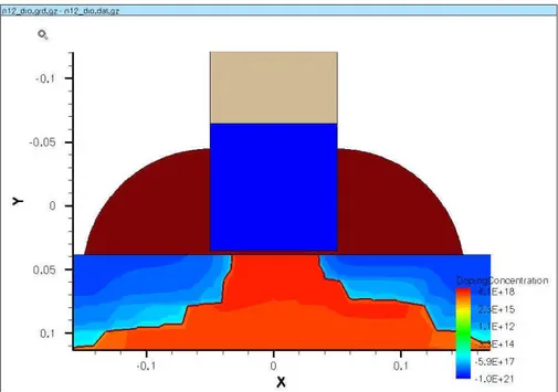
Hence, the process simulation focuses on doping profiles of S/D extensions and halo implantation. Implantation conditions and activation temperatures are also listed in Table 2.1. It is noticed that process simulation including DP technique to accomplish gate formation and asymmetric S/D extension. Besides, the capping screen oxide is formed only for source extension implantation of B+, while drain extension is implanted by BF2+ without the screen oxide. With such a procedure we
successfully obtain resembling doping distributions between junctions formation by B+ and BF2+, as shown in Fig. 2.6. Figure 2.7 shows the activated carrier
concentration of the As-doped regions, indicating that halo implantation takes part in the S/D junction construction. On account of the lateral profile which is the most influential factor in affecting the device characteristics, we enlarge the doping profiles along the channel further in Fig. 2.8. In the figure it is seen that there is no considerable difference between the asymmetric S/D extensions. Through TCAD simulation, we look forward to acquiring appropriate procedures and conditions to fabricate our practicable devices.
2.2.2 Device Fabrication and Process Flow
The devices were fabricated on 6-inch n-type (100) Si wafers with resistivity of 15~25 Ω -cm. To begin with, the N-well was formed by P+ implantation at 120 keV with dose of 7.5×1012 cm-2 and the well drive-in was carried out at 1100 ℃ for 12 hours. Then, standard local oxidation of silicon (LOCOS) process was performed with channel stop implantation by As+ at 120 keV with dose of 3×1012 cm-2 for device isolation. Threshold voltage adjustment implantation was done by As+ at 80keV with dose of 1×1013 cm-2 and anti-punch through implantation was done by P+ at 120keV with dose of 4×1012 cm-2, respectively.
Figure 2.9 illustrates the fabrication flow of PMOSFETs with major process steps in gate dielectric and electrode deposition. Briefly, after standard LOCOS process, Radio Corporation of America (RCA) clean was used for removing contaminants from the wafer surface. Subsequently, a 2.5 nm thermal gate oxide grown in N2O ambient and a 120 nm undoped poly-Si layer deposited by
low-pressure chemical vapor deposition (LPCVD) were formed in a clustered vertical furnace system sequentially. Undoped poly-Si layers were implanted with either BF2+
or B+ at 15 keV with dose of 3×1012 cm-2. Then all wafers were annealed at 900℃ for 10 seconds for dopant activation of the gate. Afterwards, a 50 nm LPCVD TEOS oxide was deposited as a hard mask layer.
Figure 2.10 shows the fabrication of asymmetric and symmetric devices. All devices were defined by G1 mask, whereas only symmetric devices received gate definition with the G2 mask before the halo implantation. The details about the halo and S/D extension implantation conditions are shown in Table 2.2. In the case of source extension implantation with B+, a 10nm TEOS oxide was capped as screen
12
oxide as mentioned previously. Source side extension of asymmetric devices and the split A of symmetric devices having extensions formed with B+ were implanted, as shown in Fig 2.11. For asymmetric devices, we defined drain-side region by G2 mask and halo implantation sequentially, as shown in Fig. 2.12. Drain side extension of asymmetric devices and the split B of symmetric devices are formed by BF2+
implantation. Afterwards, all wafers went through sidewall spacer formation, followed by a deep S/D implant with BF2+ at 15 keV at dose of 5×1015 cm-2, as shown in Fig.
2.13. Spike rapid thermal anneal (SRTA) was then carried out in N2 ambient at 1000
C to activate the dopants in the preceding implantation processes. After a typical process to deposit a 500nm TEOS passivation for humidity prevention, the metal contact pads were formed. Finally, all wafers received a forming gas annealing at 400
C for 30 minutes.
2.3 Measurement Setup
2.3.1 Electrical Measurement Setup
In our study, electrical measurements of our devices were evaluated by an HP4156A precision semiconductor parameter analyzer and an HP4284 LCR meter. The HP4156A systems were applied to gauge the current-voltage (I-V) and the HP4284 LCR systems were used for capacitance-voltage (C-V) measurements. In order to stabilize the measurement environment, black box and temperature-regulated hot chucks were employed.
2.3.2 NBTI and CHC Reliability Measurement Setup
To investigate the matching parameters of PMOSFETs before and after negative bias temperature instability (NBTI) and channel hot carrier (CHC) stresses, we have
performed the NBTI-mode and CHC-mode tests to study the performance degradation, as shown in Fig. 2.14. The stress voltages were applied by an overdrive voltage. In the NBTI-mode the stress bias was only applied to the gate whereas the other terminals were grounded. On the other hand, the CHC-mode has the applied stress biases applied to the gate and drain, while the other terminals were grounded. Temperature effect was also explored in cooperation with both NBTI and CHC modes. In the course of heating, temperature was monitored. Note that the measurement system was heated up to the objective temperature and hold for additional 30 minutes before the measurements for stabilizing the system.
2.3.3 Charge Pumping Measurements
The charge pumping (CP) measurement has been widely used to characterize the interface state density in MOSFET devices [34-35]. Both fixed amplitude sweep and fixed base sweep schemes are employed in this work to determine the density and lateral distribution of the interface traps generated during the CHC stress and NBTI stress. Figure 2.15 shows the schematic of fixed amplitude sweep CP measurement. The substrate current was measured and recorded by applying a series of voltage with fixed amplitude to the gate while both source and drain were biased with a small reverse bias and substrate was connected to ground. On the other hand, the fixed peak sweep CP measurement is used to analyze the lateral distribution of interface traps, as shown in Fig. 2.16. In this work, the CP measurement was pulsed with square-waveforms at frequency of 1 MHz, duty cycle of 50, leading and trailing of 80 nanoseconds. In the fixed amplitude sweep, the base voltage was modulated by step of 50 mV and constant pulse amplitude at 1.5 V to operate the device from accumulation to inversion. Nevertheless, the peak voltage was constant and
14
modulated pulse amplitude by step of 100 mV in the fixed peak sweep. Figure 2.17 illustrates three types of different voltage pulse applied to the gate, but we merely use the foregoing sweep to examine and analyze our devices.
Table 2.1 Process conditions for TCAD simulation
Poly Gate 120nm
N2O thermal oxide 2.5nm
Source side screen oxide 10nm Implantation conditions
N-well P+/120keV /7.5×1012 cm-2 Anti-punch through P+/120keV /4×1012 cm-2 Threshold voltage adjustment As+/80keV/1×1013 cm-2 Poly gate BF2+/15keV/5×1015 cm-2
Halo As+/50keV/1×1013 cm-2/tilt 45˚/rotation 4 times Source extension B+/5keV/5×1014 cm-2
Drain extension BF2+/5keV/5×1014 cm-2
Deep S/D BF2+/15keV/5×1015 cm-2
Rapid Thermal Annealing In N2 ambient at 1000 C for 1 second
Table 2.2 Split conditions for extension structure with the DP technique.
Halo implantation As+/50keV/1×1013 cm-2/Tilt 45˚/Twist 27˚/Rotation 4 times Symmetric
extension
Split A B+/5keV/5×1014 cm-2 Screen oxide 10nm Split B BF2+/5keV/5×1014 cm-2
Asymmetric extension
Split C Source side B+/5keV/5×1014 cm-2 Screen oxide 10nm Drain side BF2+/5keV/5×1014 cm-2
16
Chapter 3
Results and Discussion
3.1 Electrical Characteristics of Symmetric-Extension
Devices
3.1.1 Boron Penetration with Poly-Si Gate
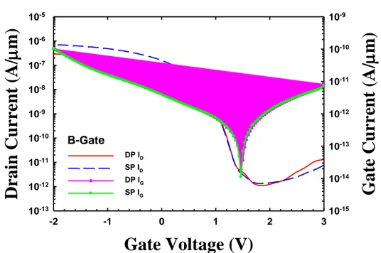
In this work, we investigate the effects of gate stack formation and fluorine incorporation on boron penetration with S/D activation temperature at 1000℃ and gate oxide down to 2.5 nm. Figure 3.1 shows the transfer characteristics of B-implanted gate with length of 10 μm. It can be seen that the Vth dramatically shifts
rightward to 0.62 V and the SS is also increased to 260 mV/dec. To verify whether DP is the culprit or not, we have also fabricated control devices with single-patterning (SP) technique as well. By single patterning we are referring to conventional self-aligned process with S/D extension formed directly after the standard gate definition. Comparisons between DP and SP splits show negligible difference, so we could exclude DP technique from being the culprit for the above abnormal Vth shift
and SS degradation. From a survey of literature, the positive shift of Vth and SS
degradation are typical behaviors of boron penetration [37]. That is, diffusion of boron from heavily-doped p+ ploy-Si gate through the thin oxide and into the underlying channel region, resulting in SS degradation and Vth shift. Furthermore, the
presence of fluorine enhances boron diffusion through thin oxide [38]. Figure 3.2 confirms this trend, i.e., for a device with BF2+-doped gate, larger Vth shift (0.72V)
and much larger gate leakage current as compared with those shown in Fig. 3.1 are observed. Such F-enhanced boron-penetration phenomenon further worsens the short-channel effects. This can be understood from the comparison of the results
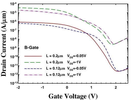
shown in Figs. 3.3 and 3.4. In the two figures it is seen that the on-state current does not increase with decreasing channel length. Moreover, Fig 3.4 shows the F-doped devices exhibit strong punch-through characteristics owing to F-enhanced boron diffusion and penetration. As a matter of fact, boron penetration through thin oxide and into the channel is detrimental to the success of surface channel PMOSFETs.
3.1.2 Accomplishment of 80nm Devices without Boron
Penetration
It has been reported that nitrided oxide prepared by oxidizing Si in an N2O
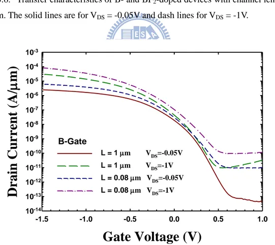
ambient shows good barrier property and blocks boron diffusion due to the pile-up of nitrogen at the Si/oxide interface (Fig. 3.5) [38]. In this work, we used RTA at 900℃ for 10 seconds to activate gate doping. Additional post-thermal process for the gate was the S/D activation step. For the reason of suppressing boron penetration, the temperature for S/D activation was reduced to 900℃. Figure 3.6 shows the transfer characteristics of devices with B- and BF2-doped gates. The channel length is 10μm.
The Vth is -0.06V and -0.78V for B- and BF2–doped gates, respectively. It is noticed
that gate leakage currents are much smaller than the results shown in Figs. 3.1 and 3.2, implying that the B-penetration has been effectively suppressed, especially for the BF2–doped split.Figure 3.7 illustrates transfer characteristics of devices with B-doped
gate and various channel length of 1 μm and 0.08 μm. The results indicate that a much better control over the short-channel effects is obtained as compared with that shown in Fig. 3.3. However, the source and drain depletion regions are so close to each other that the short-channel device still exhibits obvious short-channel behaviors such as DIBL. Another important parameter is SS which is expressed with the following equation:
18
ox dm gs ds C C q kT dV I d SS log 2.3 1 1 10 , (3.1)where Cdm is depletion layer capacitance and Cox is oxide capacitance. To get a steep
SS for better gate controllability, we need to use ultra-thin oxide to reduce Cox for
lower SS degradation in the short-channel device. A similar comparison of BF2-doped
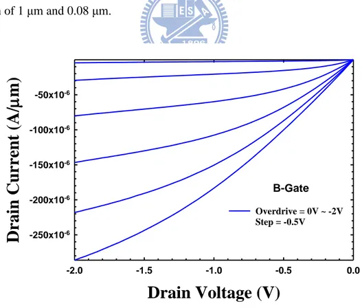
devices is shown in Fig. 3.8. In addition, the output characteristics are shown in Fig. 3.9 and Fig. 3.10, which look quite normal. The B-doped split exhibits much higher on-current than the BF2-doped one. This might be due to the lower substrate doping
with the BF2-doped one which is implied by its lower Vth, as well as the poly deletion
effect (see discussion later). The lower substrate doping could reduce the Coulomb scattering rate and improve the carrier mobility.
We also extract the Vth form the transfer characteristics at VDS = -0.05V with
several gate lengths and the results are plotted in Fig. 3.11. The Vth is defined by
constant current method, that is, the gate voltage at drain current of 10nA×(W/L), where W is the gate width, and L is the gate length. It is observed that two kinds of devices depict reverse short channel effect (RSCE) because of tilt-halo implantation which increases the doping concentration near the edge of the channel, especially in the short-channel devices [39]. Devices with B-doped gate possess more severe RSCE than the BF2-doped devices, but reveal less fluctuation in the short-channel devices.
Figure 3.12 shows the DIBL effect. It apparently exhibits worse DIBL while gate length is shrunk. SS is a key factor for switching the transistor current off, and the results are shown in Fig. 3.13 as a function of channel length. As can be seen in the
figure, SS is not severely deteriorated with gate lengths from 1 μm to 0.08 μm. Traditionally, PMOSFETs are two to three times lower in mobility than
ordinarily designed to be two to three times larger than that of NMOSFET in CMOS circuit design. One of the most important factors is the device’s driving current which determines the operation speed. Figure 3.14 shows on-state current at VG = -1.5V and
VDS = -0.05V with various gate length. The B-doped-gate split shows outstanding Ion
characteristics as compared with the BF2-doped-gate split. Hence, output
characteristics are superior as demonstrated in previous section. For comparison purpose, the transfer characteristics of a 0.1 μm NMOSFET characterized in one of our previous studies [40] are displayed in Fig. 3.15 together with 0.1 μm PMOSFETs. As can be seen in the figure, the SS values of the PMOSFETs are comparable to those of the NMOSFFTs. Nonetheless, the off-state leakage seems to be much higher for the PMOSFETs. More efforts are demanded for improving the junction characteristics. In the case of CMOS circuits, symmetrical threshold voltage is essential in circuit design. In this regard, the Vth (absolute value) seems too low for the B-doped device
and too high for the BF2-doped one. More refinement in halo doping is needed to
adjust the Vth to an appropriate value.
For better understanding of the device performance, the C-V characteristics of the devices are represented in Fig. 3.16. The measurement frequency is 100 kHz and the device area is 104 μm2. Results for the devices with severe B-penetration characterized in previous sub-section are also included in this figure. Boron penetration leading to Vth and flat band voltage shifts is confirmed. Capacitance
equivalent thickness (CET) is calculated by the following equation:
measured Si
C
A
CET
0
, (3.2)where ε0 is vacuum permittivity, εSi is silicon permittivity, A is the device gate area,
20
inversion region. The estimated CETs are listed in Table 3.1. Note that the CET extracted from the accumulation region is in good agreement with the process condition of 2.5 nm mentioned in last chapter. It also indicates that the gate depletion occurs in those devices. The CET differences between the accumulation and inversion regions of the devices are listed in Table 3.2. Among them, the device with BF2-doped
gate exhibits the most serious gate depletion. This well explains the degraded current drive of the BF2-doped split as compared with the B-doped counterpart.
3.2 Electrical Characteristics of Asymmetric-Extension
Device
In this section, we present experimental results for transistors with asymmetric S/D extension whose source and drain received different implantation and annealing conditions. Fig. 3.17 displays the device structure in which the p+ junctions are formed with either B+ or BF2+ implant. Here we define forward mode as the
measurements while the drain voltage is applied to the BF2-doped-extension side.
While reverse mode refers to the measurements with the drain voltage applied to the B-doped-extension side. An example is shown in Fig. 3.18, in which the transfer characteristics of a device with channel length of 10μm under forward and reverse modes show almost identical characteristics except the off-state leakage currents. It is observed that the leakage is anomalously high when a high drain voltage is applied to the BF2-doped-extension side. Besides, in Fig. 3.19 the output characteristics indicate
that the reverse mode exhibits a slightly higher current drive. The characteristics of the symmetrical device are exhibited in Fig. 3.20. The symmetrical device was fabricated by a self-aligned process with the S/D extensions formed by an implantation step identical to the B-doped extension of the asymmetric devices. It clarifies that there is no relationship between leakage current and the DP technique.
That is, DP technique would not induce additional etching damage. In fact, the revere mode shows severe SCEs as the channel length is reduced to 0.2μm, as shown in Fig. 3.21. As can be seen in Fig. 3.22, the output characteristic of reverse mode shows significantly punch behavior which indicates the gate losses effective control of the channel. The distinct difference in behavior is ascribed to the asymmetric junction profile, as boron diffuses more rapidly than BF2 under the same temperature, resulting
in a deeper junction for the B-doped-extension side. Our simulation results indeed confirm the results, as shown in Fig. 2.6. Nonetheless, the junction depth is underestimated and the use of the screen oxide appears to be futile. A probable explanation is oxygen enhanced diffusion (OED), resulting in enhanced boron diffusion due to the presence of the surface screen oxide [41]. The benefit of screen oxide is vanished and falls short of the purpose of forming ultra shallow junction.
Figure 3.23 illustrates the threshold voltage with the drain bias applied to different extensions. The RSCE is investigated and it resorts to the halo implantation. The halo concentration is so heavy that even the long channel devices with gate length from 10μm to 1μm depict the RSCE. However, the threshold voltage roll-off trends are observed in the asymmetric devices. The reason is that the width of channel depletion region along the horizontal direction is comparable to the channel length. A fraction of charge sharing at S/D junction is leading to threshold voltage lowering. The results imply that deeper junction is formed by boron implantation again. In contrast, BF2 extension is constructive against threshold voltage roll-off due to
shallower junction depth, as described by the forward mode measurement shown in Fig. 3.17. The results clearly indicate that boron implantation is not suitable for forming ultra shallow junction in deep-submicron devices.
22
to BF2 extension side. As shown in Fig. 3.24, the leakage currents are extremely
dependent on the drain bias, which are proportional to the electric filed on the gate and drain overlap region. When the field crowding occurs in drain junction of the device, the increased junction leakage current is called gate-induced drain leakage (GIDL). The vertical electric field at drain side is enormous when a higher drain voltage is applied. Additional evidence is the temperature effect represented in Fig. 3.25. If it is caused by the reverse-biased p-n junction, it should show strong temperature dependence. The linear current at drain bias of -0.05V fits this description, but the saturation current does not show any strong temperature dependence.
3.3 NBTI and CHC Degradations on PMOSFETs
3.3.1 Background
It is well-known that integrated circuits are inevitably operated at higher and higher temperature as the device density increases. Moreover, the scaling of gate dielectric has rendered NBTI the major factor that limits the lifetime of PMOSFETs rather than hot-carrier degradation [42]. Temperature effect and quality control of the ultrathin gate dielectric thus become serious reliability issues. In this work, we investigate the degradation of PMOS stressed under either NBTI mode or CHC mode and examine which one might cause worse degradation.
Most of current understanding about the NBTI effect is on the basis of reaction-diffusion (R-D) model [43]. The generation of interface traps and fixed oxide charges during the stress brings about the shift in threshold voltage. Holes and hydrogen (H) species generated by the Si-H bonds breaking during NBTI stress play important roles. The mechanisms are expressed as follows [44]:
Si
H
p
Si
Si
H
i
S
3 3 , (3.3)o
H
Si
O
p
H
Si
O
3
3
, (3.4)where H+ is a hydrogen ion, p+ is a hole in the inversion layer, and Ho is the neutral hydrogen atom. Equations (3.3) and (3.4) can be used to represent the generation of interface trap (Nit) and fixed oxide charge (Nf), respectively. The net contribution to
the total threshold voltage shift is thus given by
ox f it thC
N
N
q
V
, (3.5)where q is electron charge and Cox is the oxide capacitance.
In general, R-D model is used to express interface generation by the following equations [45]:
it
R H it F itk
N
N
k
N
N
dt
dN
0 , (3.6)
14 0 2 ) ( D t k N k t N H R F it , (3.7)where kF is Si-H dissociation rate constant, kR is rate of reverse annealing of Si-H, N0
is the total number of Si-H bonds, NH is hydrogen density, and DH is hydrogen
diffusion coefficient. Equation (3.7) is related to the diffusion of neutral H and shows power-law dependence with stress time.However, fixed oxide charges are arduous to charge and discharge due to their locations inside oxide. Thus, trapping or de-trapping of holes is a fast component and difficult to govern [46]. In our work, we perform conventional DC method including measure-stress-measure (MSM) technique aimed at extracting the generated interface-state density.
Hot-carrier effect has received much attention in past years. The lucky electron model is widely used to describe the observed results [47]. The worst case of hot-carrier effect for NMOSFETs usually occurs at maximum substrate current [48],
24
although still not clear for PMOSFETs. Several reports showed that the CHC effect in short-channel devices at high temperature is even worse than NBTI [49-51]. We choose the condition of CHC stress with the same voltages applied to both gate and drain at an elevated temperature to verify the aforementioned issue.
3.3.2 Channel Length and Gate Stack Dependences on NBTI
In this section, we investigate the static NBTI effect in poly-Si gated PMOSFETs. Effects of channel length and different gate stack modules are evaluated. Figure 3.26 shows threshold voltage shift versus stress time in B-gate devices. As anticipated in devices with ultra-thin gate oxide, NBTI effect is manifested with increasing temperature or decreasing channel length. The temperature effect is particularly pronounced for the short-channel device. However, the behavior seems different in BF2-gate devices, as shown in Fig. 3.27. In this figure, although NBTI effect is still
augmenting as channel length reduces at room temperature, there is no significant channel dependence at 125 ℃. The difference between the two types of devices can be interpreted by the fluorine incorporation [29][52]. Fluorine incorporation is conducive in reducing the donor-like interface traps under NBTI stress. That is, the strain at the interface is relaxed or the weak Si-H bonds are replaced by the robust Si-F bonds [53]. It has been reported that the formation of Si-F bonds could effectively decrease the generation of interface traps of NBTI due to the higher binding energy than the Si-H bonds [54]. According to the R-D model, the holes in the inversion layer at elevated temperature tend to interact with and break the Si-H bonds, resulting in the dissociation of hydrogen atoms and generation of interface traps. On the contrary, the robust Si-F bonds are less likely to be broken and generate interface traps. Note that the S/D extensions were also implanted with BF2 for the
atoms to form Si-F bonds. Therefore, the short-channel devices possess more Si-F bonds at interface in the channel as compared with the long-channel one.
In Fig. 3.28 we compare the results of the devices characterized at 125℃. Apparently the short-channel device with B-gate performs the worst among the devices. Moreover, the results indicate that long-channel devices essentially have nothing to do with fluorine incorporation. It is elucidated that both fluorine incorporation in gate and overlap regions can influence the NBTI effect. Figure 3.29 illustrates the results of charge pumping measurements performed on the long-channel B-gate devices showing that only few interface traps are generated after NBTI stress, but the short-channel device tells a quite different story in Fig. 3.30. Results of the normal and reverse lateral charge pumping measurements are shown in Fig. 3.31 Normal and reverse modes mean the source and drain side, respectively, is floating during the measurements (see the measurement setup described in Chap. 2). The results exhibit that the generated interface traps are symmetrical to the center of the channel.
3.3.3 Comparisons between CHC and NBTI Stresses
To explore the CHC effect, we apply the same overdrive voltage (V = Vth -2V)
on both gate and drain terminals while the source is grounded. Besides, we measure the currents under forward or reverse modes (see Fig. 3.32) to extract threshold voltage shift. Fig. 3.33 shows the threshold voltage shifts after CHC or NBTI stress. As can be seen in the figure, the NBTI mode shows worse degradation while the results of the CHC effects under forward or reverse modes look quite different. Figure 3.34 depicts that the CHC mode generates fewer interface traps as compared with the NBTI mode, consistent with the less voltage shift. The results of lateral charging pumping measurements are shown in Fig. 3.35. In the figure we confirm that more
26
interface traps are generated near the drain side, leading to more threshold voltage shift for the forward mode shown in Fig. 3.34. At present, the lucky electron model is not sufficient to explain the CHC effects in PMOSFETs. The reasons are that holes have a smaller impact ionization rate and a higher Si-SiO2 barrier to overcome. More
efforts are in demand for understanding the CHC effect. Finally, the NBTI effect is more serious and more attention should be paid.
Table 3.1 Capacitance equivalent thicknesses (CETs) of devices with B- or
BF2-doped gates. Devices with serious boron penetration are also included.
CET(nm) B-doped gate BF2-doped gate B-doped gate with penetration BF2-doped gate with penetration accumulation 2.7317 2.8075 2.8515 2.7485 inversion 3.1796 3.5261 3.1633 3.2015
Table 3.2 Estimated poly-depletion thickness from the difference in CETs
measured in accumulation and inversion regions.
B gate BF2 gate
28
Chapter 4
Conclusion and Future Work
4.1 Recapitulation and Conclusion
In this thesis, we have employed a novel DP technique for fabricating PMOSFETs with gate length down to 80 nm using only conventional I-line stepper. By taking advantage of the technique, devices with symmetric or asymmetric S/D extension structures were fabricated and characterized in our study. The effects of boron penetration, gate stack module, poly depletion, asymmetric extension behavior, and reliability issues, were carefully studied. Here, we briefly review and summarize the principal findings discovered in this work.
Although the DP technique requires an additional mask and extra process steps in comparison with traditional single-patterning self-aligned process, it is still an attractive alternative to fabricate deep-submicron and nano-scale devices with good CD control. TCAD simulation provides essential guidelines in combination with the DP technique, which are helpful in settling the process steps and decision on the implantation conditions.
The effects of boron penetration are scrutinized for the fabricated devices. Devices show positive shift in Vth, SS degradation, and higher gate leakage current as
the effect occurs. Moreover, fluorine enhances boron penetration so the activation temperature has to be reduced accordingly. Therefore, activation temperature plays an important role in devices demanding ultra-shallow junctions. On the other hand, BF2-gate devices exhibit severe gate depletion, causing the degraded current drive.
However, BF2 implantation is an excellent approach to achieve ultra shallow junction.
The effects of halo implantation were studied. Although devices with halo implantation show improved SCEs, increased Vth as well as more severe RSCE are
observed in short-channel devices, not to mention that halo doping is difficult to refine and optimize to an appropriate value. As for the comparison between B- and BF2-gate devices, the former shows better current drive, albeit more severe RSCE. For better performance in CMOS circuits, the B-gate devices are preferable without suffering from boron penetration enhanced by fluorine.
The asymmetric devices are attractive because they allow more margins for performance optimization. We have successfully fabricated asymmetric devices with the aid of TCAD simulation. However, the depth of B-doped junctions seems to be underestimated, owing to the use of a screen oxide which may cause undesired OED. However the off-state leakage current is reduced with such deepened junction, indicating the tradeoff between junction depth and leakage current.
We’ve also investigated reliability issues including NBTI and CHC effects with various gate stack modules. It is found that NBTI-induced degradation is worse than the CHC-induced degradation on PMOSFETs, especially in the short-channel devices stressed at a high temperature. For the BF2-gate devices, the fluorine incorporation in
both gate and overlap regions causes a reduction in the donor-like interface traps. However, fluorine enhances boron penetrations and brings about several concerns as mentioned above. By means of the CP measurements, we confirm that NBTI stress indeed generates more interface states and causes more severe degradation over CHC. For lateral CP measurements in CHC mode, we observe more interface traps are generated near the drain side, which is consistent with the larger threshold voltage shift under the forward mode of measurements. Nonetheless, our findings don’t support the observed trend reported previously by other groups that CHC would result in more severe damage than NBTI stress [49-51]. More efforts are needed to comprehend the whole picture of the PMOS reliability.

![Fig. 1.1. Historical trends of physical gate length of microprocessor unit (MPU) versus year [2]](https://thumb-ap.123doks.com/thumbv2/9libinfo/8255597.171874/53.892.152.746.118.525/fig-historical-trends-physical-gate-length-microprocessor-versus.webp)