A Study on the Properties and Modification of
Encapsulating Materials for Photoelectric Devices
A Study on the Properties and Modification of
Encapsulating Materials for Photoelectric Devices
Student Chen-Ming Chen
Advisor Dr. Tsung-Eong Hsieh
A Thesis
Submitted to Department of Materials Science and Engineering College of Engineering
National Chiao-Tung University in partial Fulfillment of the Requirements
for the Degree of Doctor of Philosophy
in
Materials Science and Engineering July 2009
- / PU-acrylate/Silica = 90 wt.%/10 wt.% - / Silicone-acrylate/Alumina = 90 wt.%/10 wt.% - / /Invar Epoxy-acrylate/Silica/Invar= 35 wt.%/50 wt.%/15 wt.% Organic Light-emitting Devices OLEDs
Organic Solar Cells OSCs Light-emitting Diodes LEDs
OLED Lithium Fluoride LiF
OLEDs
OLED 18 OLED
Turn-on Voltage = 3 V 9 V 4850 cd/m2
tris-[8-hydroxy-quinoline]aluminum (Alq3; 50 nm)/(LiF; 3 nm)/Aluminum (Al; 80
nm) NPB/ADS082BE/Bpy-OXD
OLED LED UV
Silicone-acrylate OLED LED
Half-lifetime 9 2400 98 18300
UV
- Epoxy-acrylate Nanocomposite Resins
Invar UV
OSCs OSCs
Polyethane-graft-
Glycidylmethacrylate PE-g-GMA Compatibilizer /
Polyphenylene Sulfide/Poly(ethylene terephthalate)/PE-g-GMA
PPS/PET/PE-g-GMA (wt./wt./wt.)=100/50/12.5 / 6,6/
PPS/Nylon 6,6/Glass Fiber Alloy/ PE-g-GMA(wt./wt./wt./wt.) =100/50/45/12.5
A Study on the Properties and Modification of Encapsulating
Materials for Photoelectric Devices
Student: Chen-Ming Chen Advisor: Dr. Tsung-Eong Hsieh
Department of Materials Science and Engineering, National Chiao Tung University
Abstract
This thesis studied the preparation of various ultraviolet (UV)-curable polymeric composite resins (i.e. PU-acrylate/silica (weight ratio = 90 wt.%/10 wt.%), silicone-acrylate/Alumina (weight ratio = 90 wt.%/10 wt.%) as well as epoxy-acrylate/silica/Invar (weight ratio = 35 wt.%/50 wt.%/15 wt.%) and their applications for the packaging of organic light-emitting devices (OLEDs), organic solar cells (OSCs) and light-emitting diodes (LEDs). In the part of study relating to OLEDs, the lifetimes of devices were successfully enhanced by modulating the LiF thickness and utilizing the UV-curable silicone-acrylate adhesives for encapsulation. It was found that the LiF and lab-made encapsulating adhesives can effectively block the invasion of moisture as well as oxygen in the atmosphere into the OLEDs so that an 18-folds increment of lifetimes was achieved after encapsulation. A low turn-on voltage (3 V), high luminance (4850 cd/m2 at 9 V), color/luminance tunable OLED
with device structure as ITO glass/naphthyl phenyl benzidine (NPB; 80
electroluminescent properties (e.g., hue, luminescent intensity, etc.) could be modulated by the manipulation for the layer thickness of NPB/ADS082BE/Bpy-OXD and the applied bias. In addition, the UV-curable silicone-acrylate encapsulating resin exhibited excellent gas barrier capability so that the half-lifetimes of OLEDs and LEDs reached 98 and 18300 hrs while those without encapsulation were only 9 and 2400 hrs.
The UV-curable epoxy-acrylate nanocomposite resins with good thermal stability, moderate adhesion strength and excellent gas barrier capability were also prepared in this work. In order to improve the gas blocking properties, the Invar alloy was also blended into the resins so as to increase the gas resistance and decrease resin shrinkage after UV curing. Experimental results revealed that introduction of epoxy-acrylate nanocomposite resins could effectively block the penetration of moisture as well as oxygen in the air into the devices and consequently promoted the lifetimes of OSCs.
Fabrication of polymeric reflector cups for LEDs by using polyphenylene sulfide/poly(ethylene terephthalate) (PPS/PET) and PPS/nylon 6,6/glass fiber alloys
via injection molding process was also presented in this work. In order to enhance
their mechanical properties, the compatibilizer, PE-g-GMA, was first developed by grafting the glycidyl methacrylate (GMA) into the low-density polyethylene (LDPE) with initiators by reactive extrusion procedure in a twin screw extruder. PPS/PET and PPS/nylon 6,6/glass fiber alloys with various amounts of PE-g-GMA (PPS/PET/PE-g-GMA (wt./wt./wt.)=100/50/12.5; PPS/Nylon 6,6/Glass Fiber Alloy/ PE-g-GMA(wt./wt./wt./wt.) =100/50/45/12.5) were then prepared and their physical properties as well as feasibilities for the high-brightness LEDs were also analyzed.
Contents
Abstract in Chinese--- i
Abstract in English --- iii
Acknowledgements--- v
Contents --- vi
Figure Captions --- ix
Table Captions --- xii
Chapter 1 Introduction --- 1
Chapter 2 Literature Review --- 3
2.1. Overview of Electronic Packaging Technology--- 3
2.2. Introduction of OLEDs and Their Packaging Methods --- 5
2.3. Introduction of Organic Solar Cells and Their Packaging Methods --- 8
2.4. Introduction of LEDs and Their Packaging Methods--- 9
2.5. Applications of Nanocomposites to Packaging of Electronic Devices --- 11
2.6. Motivations--- 13
Chapter 3 Experimental Methods--- 14
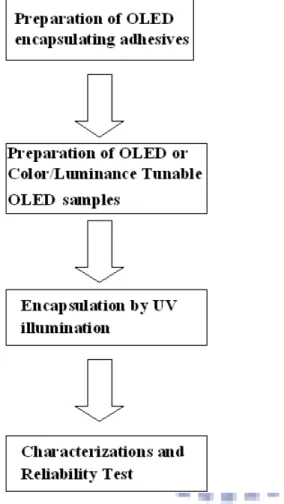
3.1. Encapsulation of OLEDs --- 14
3.1.1 Experimental Flow for Encapsulation of OLEDs --- 14
3.1.2. Materials for OLED Encapsulating Resins--- 14
3.1.3 Preparation of OLED Encapsulation Resin --- 16
3.1.4. Materials for OLED Samples--- 18
3.1.5. Preparation of OLED Samples --- 19
3.1.6 Preparation of Color/Luminance Tunable OLED Samples --- 20
3.1.7. Characterizations and Reliability Test --- 22
3.2.1 Experimental Flow for Encapsulation of OSCs --- 22
3.2.2. Materials for OSCs Encapsulating Resins--- 22
3.2.3 Preparation of OSCs Encapsulation Resin --- 23
3.2.4. Materials for OSCs Samples--- 24
3.2.5. Preparation of OSCs Samples --- 24
3.2.6. Characterizations and Reliability Test --- 25
3.3. Encapsulation of LEDs --- 26
3.3.1 Experimental Flow for Encapsulation of LEDs --- 26
3.3.2. Materials for LED Encapsulating Nanocomposites --- 27
3.3.3 Preparation of LED Encapsulating Nanocomposites --- 27
3.3.4. Materials for LED Samples --- 27
3.3.5. Preparation of LED Samples --- 27
3.3.6. Preparation of Compatibilizer for Polymer Alloys --- 28
3.3.7. Preparation of LED Reflector Cups with Polymer Alloys/Compatibilizer --- 30
3.3.8. Fabrication of LED Lamps--- 31
3.3.9. Characterizations and Reliability Test --- 31
Chapter 4 Results and Discussion --- 33
4.1 UV-assisted Synthetic Procedure --- 33
4.2 Lifetime Enhancement of OLEDs--- 35
4.3 Electroluminescent Properties of Color/Luminance Tunable OLEDs and Their Lifetime Enhancement with Encapsulation---37 4.3.1. Color Modulation and EL Effect of OLEDs with Distinct
Enhancement of OLEDs--- 44
4.4 Encapsulation of Organic Solar Cells---46
4.4.1. Polymer Matrices--- 46
4.4.2. Thermal Characterization, Gas Barrier Properties, and Electrical Conductivities of Epoxy-Acrylate Nanocomposites --- 46
4.4.3. Thermal Mechanic Properties and Adhesion Strength of Epoxy-Acrylate Nanocomposites --- 50
4.4.4. Lifetime improvement of Organic Solar Cells --- 50
4.5 Encapsulation of LEDs ---54
4.5.1. The Mechanism of Grafting Reactions for Compatibilizers --- 54
4.5.2. The Different Types of Grafting Procedure--- 55
4.5.3 . Estimation of the Percentage of Grafting for Compatibilizers---- 57
4.5.4. Dependence of Processing Parameters on Grafting Reaction of Extrusion for Compatibilizers --- 60
4.5.5. Thermal Properties of Compatibilizers (PE-g-GMA) --- 61
4.5.6 PE-g-GMA as a compatibilizer of PPS/PET and PPS/nylon 6,6/glass fiber alloys --- 62
4.5.7. Physical properties of the reflector cups for LEDs --- 65
4.5.8. Encapsulation of LEDs with Silicone-Acrylate nanocomposite -- 66
Chapter 5 Conclusions --- 69
Prospective Researches --- 71
References--- 72
Figure Captions
Fig.2-1. Typical OLED structures --- 5
Fig.2-2. Encapsulating structure for OLEDs --- 7
Fig.2-3. Encapsulating Encapsulating structure of FOLEDs for OLEDs with transparent organic/inorganic barrier coatings --- 8
Fig.2-4. Encapsulating structures for LEDs --- 10
Fig.2-5. Schematic diagram for the mechanism of oxygen/moisture resistance--- 12
Fig. 2-6. A gas diffusion model proposed by Yano et al.--- 13
Fig. 3-1. Experimental flow for encapsulation of OLEDs --- 14
Fig. 3-2. Chemical structures of monomers for the preparation of UV-curable OLED encapsulating resins--- 15
Fig. 3-3. Chemical structures of NPB, ADS082BE, Bpy-OXD, and Alq3--- 16
Fig. 3-4. Initiators and photoinitiators for the preparation of UV-curable OLED encapsulating resins--- 19
Fig. 3-5. The vacuum evaporation system for OLED sample preparation --- 20
Fig. 3-6. Structures of (a) Type 0; (b) Type I and (c) Type II OLED samples --- 20
Fig. 3-7. The structures of color/luminance tunable OLEDs. (a) Device III; (b) Device IV and (c) Device V --- 21
Fig. 3-8. Experimental flow for encapsulation of OLEDs --- 22
Fig. 3-9 Chemical structures of materials for OSCs encapsulating resins --- 23
Fig. 3-10. Chemical structures of PEDOT, P3HT and PCBM--- 24 Fig. 3-11. Structures of organic solar cells (a) prior to and (b) after encapsulation. The
Fig. 3-13. Chemical structure of monomer for the preparation of UV-curable LED
encapsulating nanocomposites--- 28
Fig. 3-14. Structures of LEDs --- 29
Fig. 3-15. Chemical structures of GMA, PE-g-Acrylic acid, and TX 101 --- 30
Fig. 3-16. The procedure used for the grafting reaction--- 31
Fig. 3-17. Chemical structures of PET, PPS, and nylon 6,6 --- 31
Fig.4-1.TEM micrographs of PU-Acrylate/silica nanocomposites --- 34
Fig.4-2.TEM micrographs of silicone-acrylate /alumina nanocomposites--- 34
Fig.4-3. Lifetimes of lab-made OLEDs (a) Type 0 and I (b) Type II --- 35
Fig.4-4. The EL spectra of Devices III: (a) NPB = 80 nm; ADS082BE = 35 nm; (b) NPB = 80 nm; ADS082BE = 50 nm; (c) NPB = 50 nm; ADS082BE = 35 nm --- 39
Fig. 4-5. The electroluminescent properties of Devices I (+: NPB = 50 nm; ADS082BE = 35 nm; : NPB = 80 nm; ADS082BE = 35 nm; : NPB = 80 nm; ADS082BE = 50 nm) --- 40
Fig. 4-6. The energy level diagrams: (a) Devices III (b) Devices IV --- 40
Fig. 4-7. The electroluminescent properties of Device IV ( : Bpy-OXD = 10 nm; : Bpy-OXD = 20 nm; : IBpy-OXD = 30 nm) --- 42
Fig. 4-8. The EL spectra of Device IV with Bpy-OXD = 20 nm at 4-9 V --- 42
Fig. 4-9. The non-stop lifetime curves for Device IV at room temperature without encapsulation and with the encapsulation of EPO-TEK OG115 as well as lab-made silicone-acrylate composite resin at 7 V --- 44
Fig.4-10. TGA of Epoxy-Acrylate nanocomposites in air --- 47
Fig.4-11. TEM micrographs of nanocomposites(a) ploymer matrices/nano-silica, (b),(c),(d) polymer matrices/nano-silica/invar --- 48
Fig.4-12. TMA of Epoxy-Acrylate nanocomposites--- 50
Fig.4-13. I-V curve of lab-made organic solar cells ((a): without encapsulation (b): with nanocomposites IV (c): with EPO-TEK 301)--- 52
Fig. 4-14. Overview of the free radical reactions --- 55
Fig. 4-15.The Different Types of Grafting Procedure --- 56
Fig. 4-16. The FTIR spectra of (a) pure LDPE and (b) PE-g-GMA --- 58
Fig. 4-17. The calibration curve for PE-g-GMA--- 59
Fig. 4-18. TGA curves of PE-g-GMA and PE-g-Acrylic acid in nitrogen ambient --- 62
Fig. 4-19. SEM micrographs of PPS/PET alloys: (a) without PE-g-GMA (b) with the PE-g-GMA --- 64
Fig. 4-20. Reflectance of the reflector cups for LEDs--- 66
Table Captions
Table 3-1. Designation of resin sample for the encapsulation of solar cells --- 24
Table 4-1. The voltage-dependent EL properties of Devices IV with Bpy-OXD = 20nm --- 43
Table 4-2. Physical properties of Epoxy-Acrylate nanocomposites --- 47
Table 4-3. Photoelectric conversion properties of lab-made organic solar cells--- 53
Table 4-4. Summary of the experimental results of grafting reactions --- 59
Table 4-5. Summary of the experimental results of PPS/PET alloys --- 63
Table 4-6. Summary of the experimental results of PPS/nylon 6,6/ glass fiber Alloys--- 65
Chapter 1
Introduction
Organic Light-emitting devices (OLEDs) are one of the important types of flat panel displays (FPDs) due to the advantages of low cost, low power consumption, high contrast ratio, fast response time, high brightness and large viewing angles [2-6]. However, invasion of moisture/oxygen may cause the oxidation of the active metal electrode as well as the thermal degradation of organic light-emitting layer during device operation. It drastically deteriorates the lifetime of OLEDs and hence a unique hermetic sealing method is required [7,8].
The demand of hermetic sealing similarly occurs in the packaging of organic solar cells (OSCs). At present, most of the researches focus on the improvement of the efficiency for solar cells; the studies relating to the packaging techniques and improvement of device lifetime are relatively less. One of the purposes of this thesis work is to develop the ultraviolet-curable (UV-curable) sealing adhesives for the packaging of above photoelectronic devices in terms of the concept of nanocomposites. In this study, we successfully synthesize several UV-curable nanocomposites and applied them for the packaging of OLEDs and OSCs. The experimental results reveal that lab-made nanocomposites exhibit good gas barrier capability, therefore prolonging the lifetimes of OLEDs and OSCs.
Light emitting diodes (LEDs) possess a widespread utilization in the fields of displays and solid-state lighting. Though inorganic, encapsulation is inevitable to ensure good reliability of LEDs for various applications. UV-curable transparent
extending their lifetimes.
Furthermore, the aluminum (Al) reflector cups of LEDs exhibit the disadvantage of high cost and insufficient reflection ratio. This work also presents polymeric-type reflector cups with low cost, high reflection ratio and easy processing method. In this part of study, polyphenylene sulfide/poly(ethylene terephthalate) (PPS/PET) and PPS/nylon 6,6/glass fiber alloys are adopted as the base materials for the fabrication of reflector cup samples. In order to enhance their mechanical properties, the compatibilizer, PE-g-GMA, was first developed by grafting the glycidyl methacrylate (GMA) into the low-density polyethylene (LDPE) with initiators by reactive extrusion procedure in a twin screw extruder. PPS/PET and PPS/nylon 6,6/glass fiber alloys contained various amounts of PE-g-GMA was then prepared and their physical properties and feasibility to the high-brightness LEDs are analyzed.
Chapter 2
Literature Review
2.1. Overview of Electronic Packaging Technology
Integrated circuits (ICs) and optoelectronic devices are made in rather dedicate manner that a supporting/protective structure is demanded in order to prevent possible damages from environment and shipping/handling during subsequent assembly process. The way to achieve such purposes, known as electronic packaging technology, is in essential to all kind of electronic products to ensure a certain level of reliability during their usage and/or operation. According to materials used and the encapsulating structure, electronic packaging can be categorized as metal packaging, ceramic packaging, and plastic packaging [9]. Among these, metal packaging and ceramic packaging are termed as hermetic packaging while plastic packaging is ascribed to the non-hermetic packaging since the highly dense microstructures of metals and ceramics enable good gas/moisture block effects in comparison with polymeric materials. However, ceramic packaging is an expensive technology since its substrate preparation and metallization processes are extremely complicated. The sealing methods for metal packaging and ceramic packaging are similar, e.g., welding, brazing, soldering or glass frit sealing; however, in spite of welding, all of them require a relatively high processing temperatures. For instance, the temperatures of soldering and glass frit sealing are as high as 200 and 400 C, respectively, which are inapplicable to the encapsulation of advanced optoelectronic products such as organic light-emitting devices (OLEDs) and organic solar cells (OSCs). Furthermore,
of contemporary electronic products.
It seems plastic packaging with the advantages such as low cost and miniaturization is the only choice for the packaging of OLEDs and OSCs, nevertheless, conventional plastic packaging utilizing thermal molding process remains inappropriate since OLEDs and OSCs cannot tolerate the severe processing conditions, e.g., high temperature, long curing duration and high pressure, during the molding process. An alternative way is to use the ultraviolet (UV)-curable resins with fast curing rate and low processing temperatures to avoid the device deterioration resulted from the thermal degradation. The encapsulation using UV curing technology hence becomes the viable way for the packaging of OLEDs and OSCs.
Acrylics resins [10] are well-known polymeric materials since they exhibit fast curing rate, high structural strength and excellent processing convenience. Their fast curing performances are suitable for specific electronic applications such as the bonding of magnets into speaker assemblies and others with high assembly line speed. Furthermore, they can be cured with heat or UV irradiation [11,12] by the addition of thermal initiators or photoinitiators, respectively. UV-curable acrylics resins have shorter curing time, weaker structure strength, and higher contraction than thermal curable ones. Although acrylics resins are good candidates for polymer matrices of organic/inorganic hybrid nanocomposites, they exhibit low viscosity. This severely restricts their practicability.
Epoxy resins [10] are also well-known polymeric materials for encapsulation because of their chemical modifiability, high transparency, good thermal stability and moderate viscosity. They are widely used in electronic, mechanic and biological industrials since the oxirane groups of epoxy resins are active to various functional groups such as alcohol, thiol, anhydride, amine, etc., facilitating the curing reactions. They can be cured with heat or UV irradiation [13] by the addition of thermal curing
agents or photoinitiators, respectively. Compared with UV curable epoxy resins, thermal curable ones have longer curing duration and the color stains when they are cured at high temperature. Despite the epoxy resins have many merits as the polymer matrices of organic/inorganic hybrid nanocomposites; they exhibit low curing rate and high brittleness after curing.
As described above, acrylics resins possess low viscosity and high contraction after curing. However, epoxy resins exhibit moderate viscosity and low contraction after curing. In addition, epoxy resins have long curing time and high brittleness after curing. Oppositely, acrylics resins possess high curing speed and low brittleness after curing. Thus, we chose these two complementary materials as the polymer matrices to modulate the physical, chemical and mechanical properties and evaluated they applicability to the encapsulation of OLEDs and organic solar cells.
2.2. Introduction to OLEDs and Their Packaging Methods
As shown in Fig. 2-1, typical OLEDs comprise of the glass substrate with indium tin oxide (ITO; anode electrode), hole-transport layer, light-emitting layer, electron transport layer, and cathode electrode [14]. The anode electrode, which may be ITO or
transparency and high hole injection capability. Moreover, the hole transport layer like naphthyl phenyl benzidine (NPB) is to diminish the energy gap between anode electrode and hole transport layer and to increase the thermal resistance [15].
OLEDs have attracted a lot of research interests because of their promising applications in flat panel displays (FPDs), solid-state lightings, etc. Compared with other competitors, e.g., liquid crystal displays (LCDs), OLEDs possess the advantages of low cost and power consumption, high contrast ratio and brightness, fast response time and large viewing angles [2-6]. For full color applications, many organic light-emitting materials have been reported. Tris-[8-hydroxyquinoline] aluminum (Alq3) and triaryl amine have been used as emitting layer and hole transport layer
respectively by Tang and Van Slyke [14]. With these two materials, the first thin-film OLED was successfully fabricated. Alq3 has been found to be a singlet host material
in the guest-host doped emitter systems and capable of blending with other dopants to give off full colors (e.g., Alq3/coumarin mixture can be modulated to irradiate blue,
orange, and green emissions.). In addition, anthracene and its derivatives have been reported to be blue emitting layers for OLEDs [16]. The requirements for cathode electrode are low work function and excellent electron injection properties (e.g., Ca, Ag, Al, Al/Li, Mg, Mg/Ag, etc.). Nonetheless, these metals cannot be exposed in the air ambient during device actuation owing to their high chemical activity. Furthermore, organic layers for OLEDs, e.g., hole-transport layer, emitting layer, electron transport layer, etc., erode during device operation while the oxygen and moisture in the atmosphere penetrate into the devices [17]. Deterioration of metal electrode and organic materials causes dark spots when the device is lighted up and drastically decreases its lifetime [7,18]. Consequently, a hermetic encapsulation is necessary for OLEDs.
OLEDs. The sealing is in fact achieved by dispersing the UV-curable resin around the active region of the device, a glass or metal lid is then flipped on the substrate, followed by a proper UV-curing treatment to accomplish the sealing. The packaging procedure is usually carried out in the atmosphere with dry nitrogen/argon or in the dry ambient (<1 ppm v/v; dew point = 76 C) [19]. In order to absorb the residual oxygen/moisture in the encapsulation or the undesired substances permeating through the encapsulating adhesive, the desiccant (e.g., calcium oxide or barium oxide) is also applied on the device side of lid [14]. Moreover, a post-thermal curing at 80 C for 1 hr is necessary to suppress the photo-polymerization, raise the crossing density, and reduce residual stress of encapsulating adhesives. Since polymeric materials exhibit less resistance to oxygen and moisture, modification of resin structure is thus indispensable to enhance the gas barrier property so as to ensure a reliable performance of OLEDs.
Fig. 2-2. Encapsulating structure for OLEDs.
In recent years, the developments of OLEDs have been switched to top-emitting
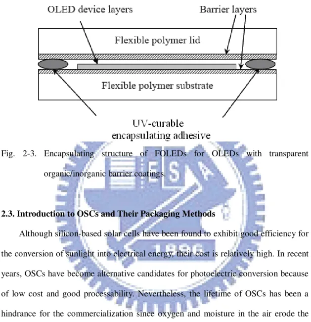
a potential solution. Fig. 2-3 [17] manifests the packaging procedure with transparent organic/inorganic barrier coating for FOLEDs.
Fig. 2-3. Encapsulating structure of FOLEDs for OLEDs with transparent organic/inorganic barrier coatings.
2.3. Introduction to OSCs and Their Packaging Methods
Although silicon-based solar cells have been found to exhibit good efficiency for the conversion of sunlight into electrical energy, their cost is relatively high. In recent years, OSCs have become alternative candidates for photoelectric conversion because of low cost and good processability. Nevertheless, the lifetime of OSCs has been a hindrance for the commercialization since oxygen and moisture in the air erode the organic materials and metal electrodes of devices, dramatically dropping the lifetime [8]. In addition, most researches focus on the improvements of OSC efficiency but the studies relating to device lifetime promotion are relatively less.
Poly(3-hexylthiophene) (P3HT) possesses good filming and excellent semiconductor characteristics such as higher carrier mobility, so that it can be applied onto a flexible plastic substrate to fabricate electro-optical devices. It can also be applied to multilayer structures according to the device requirements [20]. In 1995,
Heeger et al. used MEH-PPV mixed with [6,6]-phenyl C61-butyric acid methyl ester
(PCBM) to form a bulk heterojunction structure and obtained power conversion efficiency (PCE) of 1.5 % [21]. In 2001, Sariciftci et al. used MDMO-PPV mixed with PCBM employing LiF/Al as the cathode in an OSC and increased its PCE to 2.1 % [22]. In 2005, Yang et al. used the self organization effect in the active layer and a “slow growth” treatment to reduce the resistance of components in series connection. The carrier mobility of holes was increased and PCE raised to 4.37% [23]. In 2005, the PCE of OSC reached 5% mainly resulted from the usage of materials such as P3HT/PCBM to prepare the p-n junction structure [24]. Such kinds of OSCs exhibit the advantages of low-cost, lightweight, flexibility, and large-area processability [25]. In 2007, Jin et al. integrated the best processing conditions and added glycerol within the buffer layer to increase the short-circuit current density and PCE to 4.64% [26].
Although the literatures relating to the lifetime promotion of OSCs using metal or glass lid for encapsulation have been reported [27-29], the packaging process is rather complicated and expensive. Recently, inorganic materials such as SiO2 and
Al2O3 [30], polymers such as polyacrylics, PET, and poly(p-xylylene) [31,32] and
their combinations such as organic/inorganic hybrid composites [33] have been reported for the gas barrier application. Nevertheless, the lifetimes of OSCs packaged with these materials remain unsatisfied.
2.4. Introduction to LEDs and Their Packaging Methods
Light emitting diodes (LEDs) and relating products are widely utilized in displays and illuminations. Similarly, LEDs require packaging structures to prevent
manifested in Fig. 2-4. Epoxy resin + phosphor Blue Chip Plastic Lens Gold Wire Lead Frame Heatsink Slug Solder Connection Reflective Cups White Light Epoxy resin + phosphor Blue Chip Plastic Lens Gold Wire Lead Frame Heatsink Slug Solder Connection Reflective Cups White Light Blue Chip Plastic Lens Gold Wire Lead Frame Heatsink Slug Solder Connection Reflective Cups White Light
Fig. 2-4. Encapsulating structures for LEDs.
In order to modulate the shape of light, the reflector cups for LEDs are needed. Aluminum (Al) possesses high reflecting property so that the Al cups are extensively used for the modulation of LEDs. Nevertheless, the cost of LEDs with Al cups is high and it results undesired harsh lights.
Polyphenylene sulfide/poly(ethylene terephthalate) (PPS/PET) and the PPS/nylon 6,6 have become engineering plastics with widespread applications such as electronic parts, construction parts, etc. because of their good mechanical properties, high thermal stability, facile processibility and low cost. Recently, they are found to possess excellent reflectivity and are promising materials for reflector cups of LEDs. Nevertheless, phase separation often takes place in the cases of PPS/PET and
PPS/nylon 6,6, causing inhomogeneous blend and deteriorating the physical properties. A compatibilizer is hence required in order to solve this problem. One of the purposes of this work is to study the effects of compatibilizer types on the blending process and physical properties of PPS-based materials so that they applications to LED packaging can be realized.
2.5. Applications of Nanocomposites to Packaging of Electronic Devices
Organic/inorganic hybrid nanocomposites, which are composed of polymer matrices and inorganic fillers, have attracted lots of attentions for several decades because of their versatility in physical/chemical properties. They are used for the preservation of food as well as beverages because of the good resistance to the penetration of oxygen as well as moisture in the atmosphere [1]. Pure polymers, such as acrylics and epoxy resins, have been extensively applied for the polymer matrices of organic/inorganic hybrid nanocomposites due to their low cost, high processing facility and moderate toughness. In order to enhance the gas barrier performances of polymer matrices, inorganic fillers such as silica, metal oxide, and clay have been added [34-38]. A schematic illustration for the enhancement of oxygen/moisture resistance is shown in Fig. 2-5.
Fig. 2-5. Schematic illustration for the enhancement of oxygen/moisture resistance in organic/inorganic hybrid nanocomposites.
The inorganic fillers in the nanocomposites may effectively form the gas barrier. Yano et al. proposed a gas invasion model in exfoliated polymer/clays nanocomposites [39]. As manifested in Fig. 2-6, the total path of a diffusing gas molecule (d ) can be expressed as
W V L d d d f 2 (2-1)
where d is the thickness of a nanocomposite film, W is the width of clays, L is the length of a clay, and Vf is the volume fraction of clays. The ratio of the total path to
the thickness of a nanocomposite film, the tortuousity factor ( ), is defined as
d d
(2-2)
The permeability coefficient of composite (PC) was therefore obtained as
P C
P
P (2-3)
where PP is the permeability coefficient of the polymer matrix. Because the total path
is larger than the thickness of a resin film, the tortuousity factor would be larger than 1 and PC would hence be smaller than PP. According to this theory, the extended gas
diffusion path resulted from exfoliated clays in the nanocomposites, reducing the rate of gas permeation and allowing the inorganic filler as a permeation barrier in nanocomposite resins [40].
Figure 2-6. A gas diffusion model proposed by Yano etal. [39].
2.6. Motivations
Although conventional thermal method has been utilized for the synthesis
of encapsulating adhesives, the reaction takes several hours for completion, which is time and energy-consuming. Therefore, fast and effective preparation for package materials has become a crucial topic. Furthermore, the common encapsulating materials exhibit poor gas barrier capability, resulting in insufficient lifetimes while they are applied for package of photoelectric devices. Short lifetimes are pivotal obstacles to their commercialization.
Chapter 3
Experimental Methods
3.1. Encapsulation of OLEDs
3.1.1. Experimental Flow for Encapsulation of OLEDs
The experimental flow for encapsulation of OLEDs was illustrated in Fig. 3-1.
Fig. 3-1. Experimental flow for encapsulation of OLEDs.
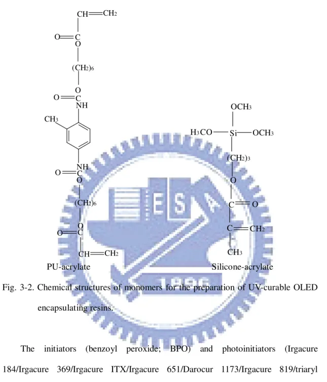
3.1.2. Materials for OLED Encapsulating Resins
Figure 3-2 illustrates the chemical structures of monomers for the preparation of UV-curable OLED encapsulating resins including PU-acrylate and silicone-acrylate. All chemicals were obtained from UCB Co. and used without further purification. Silica and alumina inorganic fillers with sizes = 30 to 100 nm were obtained from
Aldrich Co.
PU-acrylate Silicone-acrylate
Fig. 3-2. Chemical structures of monomers for the preparation of UV-curable OLED encapsulating resins.
The initiators (benzoyl peroxide; BPO) and photoinitiators (Irgacure 184/Irgacure 369/Irgacure ITX/Irgacure 651/Darocur 1173/Irgacure 819/triaryl sulfonium hexafluoroantimonate) for the preparation of UV-curable OLED encapsulating resins were purchased from Aldrich Co. and Ciba Co., respectively. Their chemical structures are depicted in Fig. 3-3 and were utilized without further
CH3 NH C O O (CH2)6 O C O CH CH2 NH O C O (CH2)6 O C O CH2 CH H3CO OCH3 OCH3 Si (CH2)3 O O C CH2 CH3 C
C O OOC O S S S+ + SF6 SF6- -O OCH3 OCH3 O CH3 CH3 OH P CH3 CH3 CH3 O O O CH3 CH3 C H3 BPO Irgacure 184
Irgacure 369 Irgacure ITX
Irgacure 651 Darocur 1173
Irgacure 819 sulfonium hexafluoroantimonate
Fig. 3-3. Initiators and photoinitiators for the preparation of UV-curable OLED encapsulating resins.
3.1.3. Preparation of OLED Encapsulation Resins 3.1.3.1. Synthesis of UV-curable PU-acrylate
PU-acrylate monomer (90 g), silica (10 g), Irgacure 184 (1 g), Irgacure 369 (0.5 g), and Irgacure ITX (0.5 g) were stirred for 30 min and irradiated by a UV lamp (100 W) for 10 min (Scheme 1). The weight-average molecular weight (Mw),
O OH O N C O N S O
number-average molecular weight (Mn), Mw/Mn ratio and viscosity of PU-Acrylate
were 153,000, 72,600, 2.11, and 16,300 cps, respectively.
Scheme 3-1
3.1.3.2. Synthesis of UV-curable Silicone-acrylate
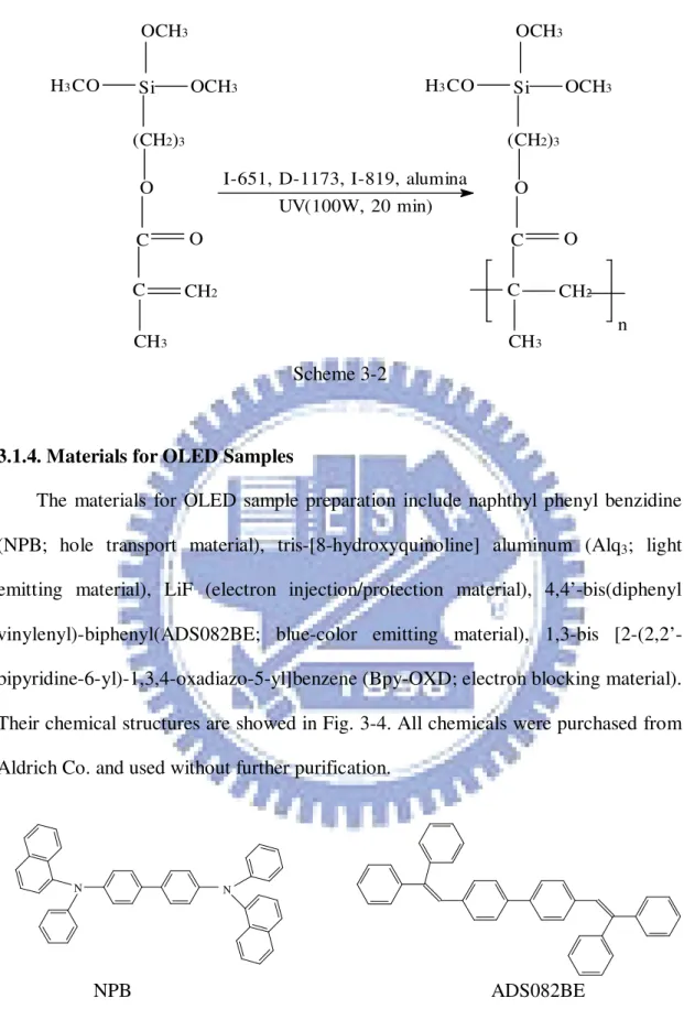
Silicone-acrylate monomer (180 g), Irgacure 651 (2 g), Darocur 1173 (1 g), Irgacure 819 (0.5 g), and alumina (20 g) were mixed for 30 min and illuminated by a UV lamp (Entela UVP; wavelength = 365 nm) at the power of 100 W for 20 min
CH3 NH C O O (CH2)6 O C O CH CH2 NH O C O (CH2)6 O C O CH2 CH CH CH2 O CO (CH2)6 O C O NH CH2 CH O C O (CH2)6 O O C NH CH3 m n photoinitiators, silica UV (100W, 10 min)
I-651, D-1173, I-819, alumina UV(100W, 20 min) C CH3 CH2 C O O (CH2)3 Si OCH3 OCH3 O C H3 n H3CO OCH3 OCH3 Si (CH2)3 O O C CH2 CH3 C N N Scheme 3-2
3.1.4. Materials for OLED Samples
The materials for OLED sample preparation include naphthyl phenyl benzidine (NPB; hole transport material), tris-[8-hydroxyquinoline] aluminum (Alq3; light
emitting material), LiF (electron injection/protection material), 4,4’-bis(diphenyl vinylenyl)-biphenyl(ADS082BE; blue-color emitting material), 1,3-bis [2-(2,2’- bipyridine-6-yl)-1,3,4-oxadiazo-5-yl]benzene (Bpy-OXD; electron blocking material). Their chemical structures are showed in Fig. 3-4. All chemicals were purchased from Aldrich Co. and used without further purification.
NPB ADS082BE
Fig. 3-4. Chemical structures of NPB, ADS082BE, Bpy-OXD, and Alq3. (continued
N N O N N N O N N N Al O N O N O N Bpy-OXD Alq3
Fig. 3-4. Chemical structures of NPB, ADS082BE, Bpy-OXD, and Alq3.
3.1.5. Preparation of OLED Samples
The OLED samples were fabricated in a glove box. Firstly, the ITO glass substrate (sheet resistance = 5 / ) was ultrasonically cleaned with the acetone, methanol, and de-ionized water for 5 min. After dried with a stream of nitrogen, baked in a oven at 120 C for 30 min and treated by O2 plasma for 90 sec, NPB (hole
transport layer; 50 nm), Alq3 (light emitting layer; 50 nm), LiF (electron injection
layer; 3 nm) and Al (cathode; 80 nm) were sequentially deposited onto the ITO glass by using a vacuum evaporator (ULVAC VPC-060) schematically illustrated in Fig. 3-5. The deposition conditions are: background pressure = 4 10 6 torr; deposition rate
of organic materials = 0.3-0.5 Å/sec; deposition rate of LiF and Al = 2-5 Å/sec. The structure of such a sample is illustrated in Fig. 3-6(a) and is denoted as Type 0 sample. In order to investigate the gas barrier effect of the LiF protection layer, 80- and 100-nm thick LiF layers were further deposited on the Type 0 sample. It was termed as Type I sample and its structure is depicted in Fig. 3-6(b). The Type II sample shown in Fig. 3-6(c) is achieved by encapsulating the resin prepared previously via
Fig. 3-5. The vacuum evaporation system for OLED sample preparation.
(a) (b) (c)
Fig. 3-6. Structures of (a) Type 0; (b) Type I and (c) Type II OLED samples.
3.1.6. Preparation of Color/Luminance Tunable OLED Samples
Firstly, the ITO glass substrate (sheet resistance = 5 / ; substrate size = 5 cm 5 cm) was ultrasonically cleaned with the acetone, methanol as well as de-ionized water for 5 min and dried with a stream of nitrogen followed by baking in an 120 C-oven for 30 min. After treated by oxygen plasma for 90 sec, NPB (50 or 80
Rotary Pump Turbo Pump VG VM VB Material Source Sensor Shutter Holder/Mask
nm), ADS082BE (35 or 50 nm), Alq3 (50 nm), LiF(3 nm), and Al (80 nm) were
sequentially deposited on the ITO glass by a vacuum evaporator illustrated in Fig. 3-5. Such a sample was designated as Device III and is illustrated in Fig. 3-7(a). The similar procedure was carried out to prepare the Device IV containing Bpy-OXD electron blocking layers with various thickness (10, 20 or 30 nm) as illustrated in Fig. 3-7(b)).
The silicone-acrylate was subsequently adopted for the encapsualtion of Device IV containing 20-nm thick Bpy-OXD via spin-coating technique (stage I: 1,000 rpm for 10 sec; stage II: 2,500 rpm for 20 sec) and cured in an UV oven (Entela UVP 2450 W) for 10 sec at room temperature. The thickness of sealing resin was approximately 50 m measured by a surface profiler (TENCOR P-10). Such a sample was termed as Device V as shown in Fig. 3-7(c).
(a) (b) (c)
Fig. 3-7. The structures of color/luminance tunable OLEDs. (a) Device III; (b) Device IV and (c) Device V.
3.1.7. Characterizations and Reliability Test of OLEDs
We measured the molecular weight, viscosity, and gas permeation rate with a GPC (Waters Alliance GPC V200), a viscosity meter (Viscolite 700), and a gas permeation meter (Illinois-8501), respectively. Moreover, the EL properties and lifetimes of OLEDs were recorded by a Keithley 2400 and Spectrascan PR650, respectively.
3.2. Encapsulation of OSCs
3.2.1. Experimental Flow for Encapsulation of OSCs
The experimental flow for encapsulation of OSCs was illustrated in Fig.3-8.
Fig. 3-8. Experimental flow for encapsulation of OSCs.
3.2.2. Materials for OSCs Encapsulating Resins
All of resin monomers, initiators, solvents and fillers (silica; 30 to 100 nm) used in the experiment were purchased from Aldrich Co. and used without further purification.
O C OCH2 O O CH2 CHC O O (CH2)6 O C O CH CH2
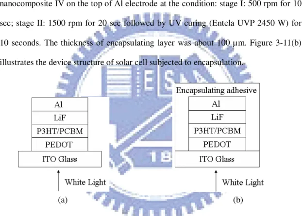
1,6-hexanedol diacrylate and 3,4-epoxycyclohexane carboxylode (see Fig. 3-9 for chemcial structures) were the monomers for acrylics and epoxy resins, respectively. BPO and triaryl sulfonium hexafluoroantimonate were utilized as thermal initiators and photoinitiators, respectively. Propylene glycol monomethyl ether acetate (PGMEA) was the solvent. The metal alloy (Invar) purchased from Goodfellow Co. was 64 wt.% Fe: 36 wt.% Ni alloy with size about 100 nm.
1,6- Hexanedol diacrylate
3,4-Epoxycyclohexane carboxylode
Fig. 3-9. Chemical structures of materials for OSCs encapsulating resins.
3.2.3. Preparation of OSCs Encapsulation Resins
1,6-Hexanedol diacrylate (10 g), benzoyl peroxide (0.1 g), and PGMEA (100 mL) were heated at 100 C for 3 hrs. After blended with 3,4-epoxycyclohexane carboxylode 10 g and triaryl sulfonium hexafluoroantimonate (0.1 g), the acrylics/epoxy resins (polymer matrices) were obtained. Then, 50 wt.% of silica and various amounts of Invar (0-15 wt.%) were added into the epoxy-acrylate polymer matrices to form the organic/inorganic nanocomposite resins. The resin sample
Table 3-1. Designation of resin sample for the encapsulation of OSCs.
Sample designation Invar content (wt.%)
Nanocomposite I 0
Nanocomposite II 5
Nanocomposite III 10
Nanocomposite IV 15
3.2.4. Materials for OSCs Samples
Polyethylene dioxythiophene (PEDOT; hole transport material),
Poly(3-hexylthiophene-2,5-diyl)(P3HT; p-type semiconductor), and [6,6]-phenyl C61-butyricacid methyl ester (PCBM; n-type semiconductor) were acquired from Aldrich Co. and utilized without further purification. Their chemical structures are illustrated in Fig. 3-10.
PEDOT P3HT PCBM
Fig. 3-10. Chemical structures of PEDOT, P3HT and PCBM.
3.2.5. Preparation of OSCs Samples
The ITO glass substrate (sheet resistance = 5 / ) was first ultrasonically cleaned with the acetone, methanol, and de-ionized water for 5 min. It was then dried by a stream of nitrogen, baked in a 120 C-oven for 30 min and treated by O2 plasma
for 90 sec. 3 wt.% PEDOT was dissolved in water, filtered with a 0.2 µm filter and deposited onto the ITO glass by spin-coating (stage I: 1000 rpm for 20 sec; stage II: 3000 rpm for 30 sec). Afterwards, the P3HT powder (molecular weight = 87,000) was
O O S n S (CH2)5CH3 n C60 O OCH3
ground together with PCBM (purity = 98%) to form P3HT/PCBM mixture (weight ratio = 1/1). Then 2 wt.% P3HT/PCBM mixture was dissolved in dichloromethane, filtered with a 0.2 µm filter, and deposited onto the PEDOT layer by spin-coating (stage I: 1000 rpm for 20 sec; stage II: 2000 rpm for 30 sec). Finally, the LiF and Al electrode were deposited onto the P3HT/PCBM by vacuum evaporator shown in Fig. 3-5. Figure 3-11(a) illustrates the device structure of solar cell prior to encapsulation.
Encapsulation of organic solar cells was achieved by spin-coating the nanocomposite IV on the top of Al electrode at the condition: stage I: 500 rpm for 10 sec; stage II: 1500 rpm for 20 sec followed by UV curing (Entela UVP 2450 W) for 10 seconds. The thickness of encapsulating layer was about 100 µm. Figure 3-11(b) illustrates the device structure of solar cell subjected to encapsulation.
(a) (b)
Fig. 3-11. Structures of organic solar cells (a) prior to and (b) after encapsulation. The
layer thicknesses of devices are: ITO glass/PEDOT(30
nm)/P3HT:PCDM(50 nm)/LiF(10 nm)/Al(80nm).
probe (Everbeing SR-4), respectively. Thermomechanic analysis (TMA), adhesion strength, and film thickness were recorded on a Seiko SSC 5000 TMA, a micro-computer universal testing machine (Hung Ta Co.) with the standard test method (ASTM D1002) and a surface profiler (TENCOR P-10), respectively. The current-voltage (I-V) curves for OSCs were measured in the air by an electric meter (Keithley 238), whose accuracy can reach picoampere, under illumination of white light from a 300 W halogen lamp (Saturn Co.) whose intensity was recorded on a radiometer (IL-1700).
3.3. Encapsulation of LEDs
3.3.1. Experimental Flow for Encapsulation of LEDs
The experimental flow for encapsulation of LEDs was illustrated in Fig.3-12.
3.3.2. Materials for LED Encapsulating Nanocomposites
The chemical structure of silicone-acrylate monomer for the preparation of UV-curable LED encapsulating resins has been manifested in Fig. 3-2. All chemicals were obtained from UCB Co. and used without further purification. The inorganic fillers including silica and alumina particles with sizes = 30-100 nm were obtained
from Aldrich Co.
3.3.3. Preparation of LED Encapsulating Nanocomposites
Silicone-acrylate monomer (180 g), Irgacure 651 (2 g), Darocur 1173 (1 g), Irgacure 819 (0.5 g), and alumina filler (20 g) were mixed for 30 min and then illuminated by a UV lamp (Entela UVP; wavelength = 365 nm) at the power of 100 W for 20 min (Scheme 2). The Mn, Mw, Mw/Mn ratio, and viscosity of silicone-acrylate
nanocomposites were 37,300, 83,200, 2.23, and 7,200 cps, respectively.
3.3.4. Materials for LEDs Samples
The blue-light GaN chips and phosphors (yttrium aluminum garnet-Y3Al5O12;
YAG) for LEDs were acquired from Tekcore Co. (Taiwan) and Nichia Co., respectively. All the materials were used directly without further purification.
3.3.5. Preparation of LED Samples
The phosphor was firstly dispersed in the silicone-acrylate encapsulating nanocomposites (phosphor:silicone-acrylate nanocomposites = 12:88 in weight ratio). Then we dripped it into the bowel of lead frame which a commercial blue chip (460
illumination for 5 min to complete the preparation of LEDs samples with structure shown in Fig. 2-4.
3.3.6. Preparation of Compatibilizer for Polymer Alloys 3.3.6.1. Materials for Compatibilizers for LEDs
The LDPE pellet (NA 20766) with density = 0.923 g/cm3 and melt index = 8
g/10 min was supplied by USI Far East Co. of Taiwan. The GMA, and PE-g-acrylic acid (PB1009), whose chemical structures were shown in Fig. 3-14, were obtained from Japanese Oil and Fat Co. and BP Performance Polymer Inc., respectively. The initiator, 2,5-dimethyl-2,5-bis(t-butyl- peroxy)hexane (TX 101) as shown in Fig. 3-13, with a half-life approximately 6 min at 160 C was purchased from the Akzo Chemie Co.
Fig. 3-13. Chemical structures of GMA, PE-g-Acrylic acid, and TX 101.
3.3.6.2. Grafting Process of GMA and LDPE for Compatibilizers
The grafting reaction was manifested in Scheme 3 and carried out by using a
C H2 C CH3 C O O CH2 O GMA PE-g-Acrylic acid CH2 CH3 CH3 CH3 CH3 CH3 CH3 CH3 C CH3 H3 C H3 OO OO TX 101 CH H2 C m n CH2 CH2 C O O H
twin screw extruder (W&P, ZSK 25). The LDPE pellets were fed at 40 g/min into the hopper and the GMA/TX 101 solution and were injected into the twin screw extruder from the injection nozzle via a liquid chromatography pump (Fig. 3-14). The extrudate was pelletized and then dried prior to analysis. The crude polymer was dissolved in hot toluene, precipitated the product with methanol, and then dried in a reduced pressure at 50 C for 24 hrs. The element analyzer (Heraeus CHN-0-Rapid F002) was used to analyze the contents of oxygen of the dried polymer. Thin film samples for Fourier-transform infrared (FTIR) analysis were prepared by pressing the precipitated resin between two mylar sheets at 120 C and 5 ton/cm2 for 1 min. FTIR
measurements were performed by using a Bio-Rad Digitlab Division UMA 300/FTS-40 spectrometer. The thermalgravimetric analysis (TGA) was carried out by using a Perkin-Elmer TGA7 and in temperatures ranging from room temperature to 470 C at a heating rate of 10 C/min in nitrogen ambient.
Scheme 3-3 C H2 C CH3 C O O CH2 O + CH2 CH2 n CH2 H2 C n TX 101 extruder
GMA LDPE PE-g-GMA
CH2 CH m CH2 C CH3 C O O CH2 O x
Fig. 3-14. The procedure used for the grafting reaction.
3.3.7. Preparation of LED Reflector Cups with Polymer Alloys/Compatibilizer 3.3.7.1. Materials for Polymer Alloys
The PET, PPS (P-4), and nylon 6,6, whose chemical structures were shown in Fig. 3-15, were obtained from Shinkong Synthetic Fibers Co., Du Pont Co., and Phillips Petroleum Co., respectively.
Fig. 3-15. Chemical structures of PET, PPS, and nylon 6,6.
3.3.7.2. Manufacture of LED Reflector Cups
PPS powder, PET or nylon 6,6 pellets/glass fiber, TiO2 powder, and the PE-g-GMA compatibilizer were mixed in the twin screw extruder at 280 C at a screw
speed of 300 rpm. After the extrudate was then cooled, palletized, and injection-molded, the polymeric reflector cups were manufactured as shown in Fig. 3-16. C O C O O C2H4 O n PET S n PPS nylon 6,6 N C O H (CH2)4 C O (CH2)6 H N n
Fig. 3-16. Polymeric reflector cups for LEDs.
3.3.8. Fabrication of LED Lamps
The LEDs samples fabricated previously (see Sec. 3.3.5) were placed into the polymeric reflector cups for form the LED lamps as shown in Fig. 3-17.
Fig. 3-17. Structures of LED lamps
3.3.9. Characterizations and Reliability Test of LEDs
We measured the viscosity and molecular weight with a viscosity meter (Viscolite 700) and a GPC (Waters Alliance GPC V200), respectively. The transparency, refractive index, and gas penetration were examined with a UV/Visible spectrometer (HITACHI U-3300), a ellipsometry (Filmetrics F20), and a gas
(Spectrascan PR650).
Impact test specimens were prepared by an injection molding machine (Toshiba IS55). Izod impact test was conducted on unnotched specimens at 25 C according to ASTM D256 test standard. Morphologies of fractured surfaces of PPS/PET alloys were examined by scanning electron microscopy (SEM, Cambridge model S360).
Chapter 4
Results and Discussion
4.1. UV-assisted Synthetic Procedure
Ultraviolet (UV) light is the high-energy electromagnetic radiation with wavelength ranging from 180 to 400 nm. The main principle of UV-assisted synthetic procedure is to induce the dissociation of photoinitiators, generating free radicals to result in initiation, propagation and termination for photo-polymerization [15]. Scheme 3-1 and 3-2 present the UV-assisted synthetic procedure of encapsulating adhesives. In this study, the reactions of PU-acrylate and silicone-acrylate with UV-assisted synthetic procedure takes only 10-20 min, while that with conventional thermal methods takes several hours for completion. Moreover, the viscosities of PU-acrylate and silicone-acrylate prepared by UV irradiation (16,300 cps for PU-acrylate; 7,200 cps for silicone-acrylate ) are larger than that prepared by conventional thermal methods (8,500 cps; reaction duration = 8 hrs for PU-acrylate and 5,300 cps; reaction duration = 20 hrs for silicone-acrylate ) and no solvent is necessary in the UV-assisted synthetic procedure. These advantages fit the requirements for the low-cost and clean production of encapsulating adhesives or other polymeric materials.
Moreover, the silica and alumina particles were well dispersed in polymer matrices (Figures. 4-1 and 4-2), thus the gas penetration can be improved.
475 nm
95 nm 475 nm
95 nm
Fig.4-1. TEM micrographs of PU-acrylate/silica nanocomposites.
95 nm
475 nm 95 nm
475 nm
4.2. Lifetime Enhancement of OLEDs
As shown in Fig. 4-3(a), the lifetimes of OLED samples are strongly affected by the thickness of the protection layer, LiF. Without LiF, the luminance sharply drops when the device is lighted up and the half-lifetime, defined as the duration while the luminance decays from the original amount to its half, is only 4 hrs, revealing the oxygen and moisture in the air deteriorate the metal electrodes and organic layers. When LiF is deposited, however, the half-lifetime drastically rises to be 20 (LiF = 80 nm) and 31 hrs (LiF = 100 nm), respectively, representing the LiF has the resistance of the oxygen and moisture in the air and thus the lifetimes of lab-made OLEDs are prolonged. Experimental results manifest that the lifetimes of OLEDs can be modulated with the LiF thickness and the devices with thicker LiF films exhibit better barrier effects.
(a) (b)
Although the half-lifetimes of lab-made OLEDs have been promoted to reach 31 hrs, it remains unsatisfied. In order to further improve the lifetimes, lab-made encapsulating adhesives were spin-coated in the OLED devices and cured with the UV illumination as shown in Fig. 3-6(c). The LiF layer inserted between the cathode and the encapsulating adhesives not only exhibits the gas penetration as described above but also avoids the corrosion of encapsulating adhesives (i.e. PU-acrylate), which are slightly acidic, on the cathode (Al layer). As shown in Fig. 4-3(b), application of encapsulating adhesives dramatically enhances the half-lifetimes of OLED devices to 72 hrs, which are 2.3 folds to those of Type I (LiF = 100 nm) and 18 folds to those without encapsulation (Type 0). This result shows that the encapsulating
adhesives can further block the entry of moisture and oxygen in the air into the OLEDs, suppressing the degradation of organic materials and metal electrodes. In comparison with commercial UV curable epoxy-based encapsulating adhesives (EPO-TEK OG112-4; Epoxy technology Inc.), the nanocomposite encapsulating adhesives exhibit longer lifetimes and shorter curing duration since the half-lifetimes and curing times of EPO-TEK OG112-4 are 35 hrs and 2 min, respectively. This indicates that PU-acrylate can be an alternative polymer matrix to epoxy resins for the encapsulation of OLEDs via the appropriate prescription of photoinitiators and dispersion of fillers. Compared with the literature data for the lifetimes of OLEDs [40], our OLED devices with multi-layer encapsulation exhibit better gas blocking capability since the half-lifetimes of devices with packages reported in the literature are only 3.1 folds to those without packages.
Experimental results have proved that LiF and lab-made encapsulating adhesives for OLEDs encapsulation have better lifetime enhancement than other known materials because PU-acrylate exhibits better water proof propensities than other
polymers [15] and high adhesion strength with LiF [10]. Moreover, LiF has tougher chemical resistance to encapsulating adhesives than other inorganic materials [41]. Consequently, the encapsulation combining the LiF and PU-acrylate can effectively reduce the gas permeability. In the near future, synthesis of UV-curable encapsulating adhesives with different polymer matrices and fillers will be carried out in order to further improve the lifetimes of OLEDs.
4.3 Electroluminescent Properties of Color/Luminance Tunable OLEDs and Their Lifetime Enhancement with Encapsulation
4.3.1. Color Modulation and EL Effect of OLEDs with Distinct NPB/ADS082BE Layer Thicknesses
As shown in Figs. 4-4(a)-(c) as well as Fig. 4-5, the EL hue and luminance of OLED samples strongly depend on the thickness of NPB (hole transport layer) and ADS082BE (blue-color emitting layer). With the bias voltage = 7 V and the NPB thickness = 80 nm, the OLED with thinner ADS082BE (35 nm) emits blue light (CIEx,y = (0.18,0.27)) and that with thicker ADS082BE (50 nm) emits deep-blue light
(CIEx,y = (0.12,0.20)). Moreover, the luminance of former (350 cd/m2) is higher than
that of the latter (10 cd/m2). This result indicates that the device with thicker
ADS082BE can effectively confine all the holes in the ADS082BE layer, whose emitting efficiency is lower, so that the recombination almost takes places in the blue-color emitting layer; however, the device with thinner ADS082BE cannot completely restrict the holes in the ADS082BE layer and some holes can overcome
(Alq3), whose emitting efficiency is higher, inducing the red-shift of EL color and
strong luminance.
When the layer thickness of NPB was reduced to be 50 nm, nevertheless, the OLED with thinner ADS082BE (35 nm), which is lighted up at 7 V, irradiates blue-green light (CIE x,y = (0.23,0.30)), revealing the decrease for electrical resistance
of NPB can further increase the mobility of hole and raise the possibility of the recombination in the Alq3 layer. In addition, its luminance (450 cd/m2) at 7 V is
highest among Device III due to its lowest electrical resistance. Since the EL efficiencies of NPB as well as ADS082BE are diverse and the location of recombination can be manipulated by the layer thickness of NPB/ADS082BE, the color/luminance tunable OLEDs can thus be fabricated.
Fig. 4-4. The EL spectra of Devices III: (a) NPB = 80 nm; ADS082BE = 35 nm; (b) NPB = 80 nm; ADS082BE = 50 nm; (c) NPB = 50 nm; ADS082BE = 35 nm.
(a) (b)
Fig. 4-5. Electroluminescent properties of Devices I (+:NPB = 50 nm; ADS082BE = 35 nm; :NPB = 80 nm; ADS082BE = 35 nm; :NPB = 80 nm; ADS082BE = 50 nm)
(a) (b)
Fig. 4-6. The energy level diagrams for (a) Devices III and (b) Devices IV.
-6 -4 -2 0 2 4 6 8 10 12 0.1 1 10 100 1000 10000 Lu m in an ce (c d/ m 2 ) Voltage(V)
4.3.2. Introduction of Electron Blocking Layer
In order to promote the EL properties of blue-light OLEDs (i.e., Device III containing 80 nm NPB and 35 nm ADS082BE), Bpy-OXD (the electron blocking layer) was introduced into the device. Without Bpy-OXD, the electron can freely arrive at either ADS082BE or Alq3 layer and the recombination occurs when the hole
and electron meet as shown in Fig. 4-6(a). With Bpy-OXD, however, the hole can be impeded in the boundary of Bpy-OXD/Alq3 since it cannot overcome the energy
barrier between the Bpy-OXD and Alq3 as shown in Fig. 4-6(b) [43] and the
recombination consequently takes place in the Alq3 layer, whose emitting efficiency is
higher, irradiating strong luminance. As shown in Fig. 4-7, introduction of Bpy-OXD can drastically not only raise the luminance but also lower the turn-on voltage to 3V, whereas the turn-on voltage of the OLED without Bpy-OXD is 5V. This illustrates that Bpy-OXD may hinder the entry of holes into the Alq3 layer and the
recombination readily occurs while electrons arrive at Alq3/Bpy-OXD boundary,
decreasing turn-on voltage. Despite of the addition of Bpy-OXD into OLEDs may heighten the EL intensity, the OLED with 30-nm thick Bpy-OXD exhibits weaker luminance (60 cd/m2 at 4 V; 650 cd/m2 at 7 V) than that with 20-nm thick Bpy-OXD (200 cd/m2 at 4 V; 1550 cd/m2 at 7 V). This result comes from that the hole may be
trapped in the Bpy-OXD layer while the layer thickness of Bpy-OXD is larger than 20 nm, causing the electrical resistance is high enough to obstruct the migration of the hole and lessen the recombination in the Alq3 layer.
Furthermore, we observed the voltage-dependent EL effect in Device IV containing 20-nm thick Bpy-OXD. As shown in Fig. 4-8 and Table 4-1, the EL spectra
may accelerate and the recombination zone gradually locates in the ADS082BE layer (blue emitting layer) when the applied voltage is increased. This induces the change of EL hue from deep green to light blue.
Fig. 4-7. Electroluminescent properties of Device IV ( :Bpy-OXD = 10 nm; :Bpy-OXD = 20 nm; : Bpy-OXD = 30 nm).
Fig. 4-8. EL spectra of Device IV with Bpy-OXD thickness = 20 nm at 4-9 V.
-6 -4 -2 0 2 4 6 8 0.1 1 10 100 1000 10000 Lu m in an ce (c d/ m 2 ) Voltage(V)
Table 4-1. The voltage-dependent EL properties of Devices IV with Bpy-OXD thickness = 20 nm.
Applied voltage (V) CIEx,y Luminance (cd/m2) EL color
4 (0.30, 0.55) 200 Deep green 5 (0.28, 0.50) 350 Green 6 (0.26, 0.46) 700 Light green 7 (0.24, 0.40) 1550 Green-blue 8 (0.22, 0.34) 3900 Blue-green 9 (0.20, 0.30) 4850 Light blue
Although the modulation of EL colors for OLEDs can be executed by the modification of light-emitting materials, the process for the tune of colors by the variation of layer thickness, introduction of electron blocking layer and manipulation of applied voltage is relatively ease, cheap, and convenient. Nonetheless, as shown in Fig. 4-9, the luminance drastically decreases when Device IV (NPB = 80 nm; ADS082BE = 35 nm; Bpy-OXD thickness = 20 nm) without encapsulation is actuated at 7 V and the half-lifetime is only 9 hrs, representing the moisture and oxygen in the ambient lead to the corrosion of organic layers and Al electrode. To further improve the lifetimes of OLEDs, we synthesized the encapsulating resin with high gas barrier capability and applied it for the package of lab-made OLEDs.
Fig. 4-9. Lifetime curves for Device IV at room temperature without encapsulation and with the encapsulation of EPO-TEK OG115 as well as lab-made silicone-acrylate composite resin at 7 V.
4.3.3. UV-curable Encapsulating Resin and Its Application for Lifetime Enhancement of OLEDs
In recent years, lifetime improvements of OLED packages with cover glass [28,29] or organic/inorganic multilayer (e.g., Barix technique developed by Vitex Systems Co., etc.) [37] have been reported. Although the gas blocking performances of cover glass and organic/inorganic multilayer are good, their encapsulation procedures are high-cost and complicated. Consequently, a package of OLEDs with the low-cost UV-curable composite adhesive comprised of silicone-acrylate polymeric matrix and alumina inorganic filler is developed in this work.
Figure 4-9 shows the lifetime measurement of Device IV without encapsulation and with the encapsulation of EPO-TEK OG115 (Epoxy technology Inc.) as well as the silicone-acrylate composite resin at room temperature. Furthermore, all the luminance measurements versus time were carried out in a non-stop manner at constant voltage (7 V). The half-lifetimes of OLEDs with silicone-acrylate composite resin is substantially improved to 98 hrs in comparison with 9 hrs for that without package, showing that the silicone-acrylate composite resin can effectively restrict the permeation of moisture and oxygen in the air into the devices. The gas resistance of silicone-acrylate composite resin suppresses the degradation of Al electrode as well as organic materials and eventually increases the lifetimes. Compared with the commercial packaging adhesive (EPO-TEK OG115), the silicone-acrylate composite resin exhibits better gas barrier capability and shorter curing time because the half-lifetimes and curing time of OLEDs with EPO-TEK OG115 are 41 hrs and 5 min, respectively. Experimental results manifest that the composite sealing resin, which consists of silicone-acrylate matrix, finely dispersed alumina fillers and proper prescription of photoinitiators, possesses good gas barrier property than the commercial available epoxy resins-based materials.
4.4. Encapsulation of OSCs
4.4.1. Polymer Matrices of Encapsulation Resins
Although 1,6-hexanedol diacrylate exhibits good mechanic properties, low brittleness after curing, and short curing time, it possesses weak thermal stability, low viscosity and high contraction after UV curing. In contrast, 3,4-epoxycyclohexane carboxylode is a superior cycloaliphatic epoxy resin with high thermal resistance, good transparency, low dimension change and moderate viscosity. In addition, the cycloaliphatic epoxy resin has lower chloride content than other epoxy resins because it is synthesized by peroxidation rather than by the reaction of hydroxyl group and epichlorohydrin [10]. The chloride ion may cause the erosion of the electronic devices in humidity. Therefore, we blended 3,4-epoxycyclohexane carboxylode with the acrylics resin to heighten the thermal resistance, diminish the shrinkage and increase the viscosity.
4.4.2. Thermal Characterization, Gas Barrier Properties, and Electrical Conductivities of Epoxy-Acrylate Nanocomposites
TGA characterization of epoxy-acrylate nanocomposites was executed in air and the result is depicted in Fig. 4-10. Their decomposition temperatures (Td; at 5%
weight loss) are tabulated in Table 4-2, revealing they have excellent thermal stabilty since all Td’s are higher than 300 C. This is very crucial on the encapsulation of the
electronic device because they can endure high temperature and resist the penetration of gas despite the electronic device liberates much heat when actuated.
Fig. 4-10. TGA profiles of epoxy-acrylate nanocomposite resins in air.
Table 4-2. Physical properties of Epoxy-Acrylate nanocomposites.
Sample Td
( C) Adhesion strength (kgf/cm2) Gas penetration (%) Electrical conductivity (S/cm)
Nanocomposite I 345 117.5 10.71 1.5 10 12
Nanocomposite II 340 107.4 8.17 2.3 10 10
Nanocomposite III 328 90.7 7.34 4.7 10 10
The organic/inorganic nanocomposites exhibit good gas resistance and the introduction of Invar drastically promotes the gas barrier effect as shown in Table 2. Moreover, the gas peneration decreases with the increase of Invar because the polymer matrices/nano-silica were well dispersed (Fig. 4-11(a)) and the metal alloys lying on the polymer matrices/nano-silica may further fill in the vacancy of the polymer matrices/nano-silica and thus the gas penetration can be improved (Figs. 4-11(b)-(d)).
Fig. 4-11. TEM micrographs of nanocomposites(a) ploymer matrices/nano-silica, (b),(c),(d) ploymer matrices/nano-silica/invar
We also have investigated the electrical conductivities of the nanocomposites
(a) (b)
samples as shown in Table 4-2. The electrical insulation is essential to avoid electrical interference when the device is actuated.
4.4.3. TMA Properties and Adhesion Strength of Epoxy-Acrylate Nanocomposites
As shown in Table 4-2 and Fig. 4-12, addition of Invar not only enhances the gas barrier capability but also reduces the shrinkage. Furthermore, the dimension change in planar direction decreases with the increase of Invar as shown in the TMA profiles of Fig. 4-12. Nevertheless, the adhesion strength drops with the raising of Invar owing to the poor adhesion between metal with the glass.
Fig. 4-12. TMA profiles of epoxy-acrylate nanocomposites.
4.4.4. Lifetime Improvements of OSCs
exhibits the photoelectric conversion properties initially and its efficiency is 0.42 %. As the actuating time proceeds, nonetheless, the photoelectric conversion capability gradually decays. This is ascribed to the invasion of moisture and oxygen in the atmosphere into the device, causing the corrosion of organic materials and metal electrode. After actuating for 48 hrs, the efficiency reduces to 0.016% with a decay ratio = 96.2 %.
In order to improve the lifetime of OSCs, we applied nanocomposites IV for the device package. With the encapsulation, as manifested in the Fig. 4-13(b) and Table 4-3, the decay ratio sharply improves and is only 13 and 37% when the actuating time are 15 and 48 hrs, respectively. The result indicates that nanocomposites IV is capable of resisting the penetration of oxygen as well as moisture in the air into the device, effectively prolonging the lifetime of OSCs. Similar result can also be observed in the case of commercial encapsulating adhesive (EPO-TEK 301, Epoxy Technology Co.) as shown in Fig. 4-13(c) and Table 4-3. Compared with the photoelectric conversion properties of organic solar cells with EPO-TEK 301, the decay ratio of the device with the package of nanocomposites IV is lower, revealing that the nanocomposites IV exhibits better gas barrier capability than EPO-TEK 301.
Fig. 4-13. I-V curves of OSC samples (a) without encapsulation (b) with nanocomposites IV and (c) with EPO-TEK 301.
(a) (b)