IEEE PHOTONICS TECHNOLOGY LETTERS, VOL. 16, NO. 8, AUGUST 2004 1807
Highly Reliable GaN-Based Light-Emitting Diodes
Formed by p–In
0:1
Ga
0:9
N–ITO Structure
Kow-Ming Chang, Jiunn-Yi Chu, and Chao-Chen Cheng
Abstract—Indium–tin–oxide (ITO) is deposited as a transparent
current spreading layer of GaN-based light-emitting diodes (LEDs). To reduce the interfacial Schottky barrier height, a thin p In0 1Ga0 9N layer is grown as an intermediate between ITO and p-GaN. The contact resistivity around 2.6 10 2 cm2 results in a moderately high forward voltage LED of 3.43 V operated at 20 mA. However, the external quantum efficiency and power efficiency are enhanced by 46% and 36%, respectively, in comparison with the conventional Ni–Au contact LEDs. In the life test, the power degradation of the p–In0 1Ga0 9N–ITO contact samples also exhibits a lower value than that of the conventional ones.
Index Terms—GaN, indium–tin–oxide (ITO), In0 1Ga0 9N, light-emitting diodes (LEDs).
I. INTRODUCTION
G
ROUP III-nitride semiconductors have attracted much attention for their versatile applications recently [1], [2]. A high-brightness GaN-based light-emitting diode (LED) is an interesting issue because of its important role in full-color dis-play and lighting applications [3], [4]. Following the successful demonstration of p-type conductivity on Mg-doped GaN by post-growth thermal annealing in nitrogen ambience, blue and green LEDs become real and commercially available [5]. How-ever, poor conductivity of p-GaN layer still limits the current spreading, and it is necessary to deposit a conductive layer for current spreading. This layer should form good ohmic contacts to p-GaN and be transparent to the emitted light from the active layer. In the past, much work focused on materials and methods to form good contacts to p-GaN [6]–[8]. Among these studies, Ni–Au is usually used as a semitransparent current spreading layer due to its good contact characteristics. However, Sheuet al. [9] showed that the transmittance of semitransparent
Ni–Au films for blue LEDs is only about 60% to 85% in the 450–550-nm wavelengths. To improve the transmittance, it is feasible to replace the conventional Ni–Au contact by a better transparent conductive contact. Nowadays, transparent conduc-tive oxide materials (TCO), such as indium–tin–oxide (ITO), aluminum-doped zinc–oxide (AZO), and cadmium–tin–oxide (CTO), are widely applied to optical electrical devices [10], [11]. There are also several studies [12]–[15] discussing the
Manuscript received February 10, 2004; revised April 12, 2004. This work was supported by the National Science Council, Taiwan, R.O.C., under Contract NSC 92-2215-E-009-065.
K.-M. Chang and J.-Y. Chu are with the Department of Electronics Engi-neering and Institute of Electronics, National Chiao Tung University, Hsinchu, Taiwan 300, R.O.C.
C.-C. Cheng is with Highlink Technology Corporation, Hsinchu, Taiwan 300, R.O.C.
Digital Object Identifier 10.1109/LPT.2004.830523
applications of ITO to GaN-based LEDs. Margalith et al. [12] obtained the Schottky but not ohmic characteristics of the ITO–p-GaN interface after thermal annealing. This result could be attributed to a large work function difference between ITO and p-GaN. In order to improve the contact characteristics, some authors added an interfacial layer such as Ni or NiO before ITO deposition by a little sacrifice of transparency [13]–[15]. In this letter, we demonstrate a thin p–In Ga N layer as an intermediate between ITO and p-GaN to form a nearly ohmic contact. The LEDs with this structure exhibit excellent reliability under a 50-mA current stress.
II. EXPERIMENTS
The InGaN–GaN multiquantum-well (MQWs) LED wafers were grown on c-face sapphire substrates by a metal–or-ganic chemical vapor deposition (MOCVD) system. The epitaxial structure comprised 4- m-thick n-GaN 0.1- m-thick InGaN–GaN (MQW) active layer, and 0.1- m-thick p-GaN. Moreover, the carrier concentrations of the p-GaN and n-GaN were 5 10 and 3 10 cm , respectively. A wafer with a peak wavelength at 465 nm was chosen and cut into four pieces. One piece was prepared for the conventional LEDs with Ni–Au contact, and the other three were reloaded into the same MOCVD chamber to grow a 10-nm-thick p-In Ga N layer for LEDs with ITO contacts.
GaN-based LEDs 300 300 m with different conducting layers were fabricated. We first used an inductance-coupled plasma (ICP) etcher to form mesa structures and immersed these samples in H SO H O and NH OH H O solutions. Next, ITO (280 nm) was deposited on the p–In Ga N/p–GaN sam-ples by E-beam evaporator at 300 C in oxygen ambience with a partial pressure of 5 10 torr, and the Ni–Au (4 nm/4 nm) was deposited on the p-GaN sample by E-beam evaporator with a base pressure of 2 10 torr. The In Ga N–ITO contact samples were subsequently annealed at 500 C and 600 C in nitrogen ambience. As for the Ni–Au contact sample, it was annealed at 540 C in nitrogen ambience to achieve the optimal ohmic contact to p-GaN. Cr–Au 0.08 m 0.8 m metallization was employed for the n-type contact layer, p-and n-bonding pads. Test keys consisting of transmission line model (TLM) patterns were used to measure the contact resistivity of the conducting layers on p-GaN. The pad size is 300 80 m and the spacings were ranged between 2 and 20 m. The current–voltage characteristics were measured at room temperature by an HP-4156 analyzer with a current source. After measuring, these samples were subsequently polished, scribed, and sliced into chips. We chose ten chips per sample to package into TO–Can forms. A Keithley 2430 source
1808 IEEE PHOTONICS TECHNOLOGY LETTERS, VOL. 16, NO. 8, AUGUST 2004
Fig. 1. Transmittance spectra of the blank p–i–n GaN–sapphire, the ITO, and Ni–Au films deposited on p–i–n GaN–sapphire under different annealing conditions (n at 470 nm= 1:8, n at 470 nm= 2:5).
meter was connected with an integrating sphere to measure the current–voltage and current–power characteristics of these LEDs. During the reliability testing, these chips with TO–Can form were stressed by a 50-mA current injection at room temperature and relative humidity of 40%.
In order to truly exhibit the effects of absorption, internal re-flection and interference of the conducting films on GaN-based LEDs, the p–i–n GaN with a double-side-polished sapphire sub-strate was used in the transmittance measurement. The trans-mittance spectra of these samples were measured by a Hitachi U3010 spectrophotometer.
III. RESULTS ANDDISCUSSION
Fig. 1 shows the transmittance of the p–i–n GaN–sapphire ITO and Ni–Au layers deposited on p–i–n GaN–sapphire samples with different annealing temperatures. Due to the great difference of the optical index between GaN and air, the blank sample with p–i–n GaN–sapphire structure exhibits relatively poor transmittance. The curves of ITO samples annealed at 500 C and 600 C are nearly coincident, and the light trans-mittance at 465 nm is 83% while the Ni–Au sample shows only 61% due to the high extinction coefficient of Ni and Au. It is supposed that ITO can extract more light than the conventional Ni–Au layer does.
Fig. 2 presents the current–voltage characteristics of different contacts on p-GaN. The Ni–Au sample exhibits a linear ohmic property, while the sample of p–In Ga N–ITO shows a nearly linear ohmic characteristic after annealing at the temper-ature of 500 C, which is the optimal condition. As shown in Fig. 3, the contact resistivity of Ni–Au contact decreases from 8 10 cm to 3 10 cm with increasing the current density from 0 to 50 A cm . As for the p–In Ga N–ITO contact samples, the contact resistivity reduces from 2 10 to 2.5 10 cm with raising the current density from 0 to 50 A cm . The results imply that both the interfaces of p-GaN with Ni–Au and p-In Ga N–ITO contacts are not ideal ohmic contacts, but the former exhibits better contact
Fig. 2. I–V characteristics of p–In Ga N–ITO contacts annealed at 500 C and 600 C and N–Au contact annealed at 540 C on p-GaN.
Fig. 3. Contact resistivity as a function of injection current density.
property than the latter. Moreover, this figure also indicates that the contact resistivity is 2.6 10 cm under a current density of 27 A cm , which is equivalent to a current of 20 mA applied in the normal LED operation. This result shows that the p–In Ga N–ITO contact is good enough to be used in LED application.
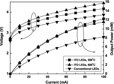
Both forward voltage and output power increase with ele-vating the current as demonstrated in Fig. 4. At the current of 20 mA, the forward voltage and output power are 3.43 V and 4.30 mW for chips with p–In Ga N–ITO contacts annealed at 500 C, respectively. On the other hand, the conventional chips with Ni–Au contacts show 3.21 V and 2.95 mW. It is es-timated that p–In Ga N–ITO LED can enhance the external quantum efficiency and power efficiency by about 46% and 36% at 20 mA, respectively. This improvement is definitely attributed to the high-transparent contacts and relatively low contact resis-tance.
From the results of life test shown in Fig. 5, the conven-tional Ni–Au samples would suffer the output power decay of 27% after 1008-h stress and the 500 C annealed ITO samples
CHANG et al.: HIGHLY RELIABLE GaN-BASED LIGHT-EMITTING DIODES 1809
Fig. 4. Measured forward voltage and output power as functions of injection current of GaN-based LEDs with p–In Ga N–ITO and Ni–Au contacts.
Fig. 5. Room temperature life test of degradation of output power from GaN-based LEDs with p–In Ga N–ITO and Ni–Au contacts.
showed a similar decay of 25%. However, the light power was deteriorated by 36% for the p–In Ga N–ITO samples an-nealed at 600 C. This result is probably due to the poor contact property which will induce a severe heating effect under high current injection. Besides, the surface morphology of 600 C ITO films seemed to contain a lot of pits and defects.
IV. CONCLUSION
This letter presents highly transparent and nearly ohmic contacts of p–In Ga N–ITO on p–GaN and exhibits the excellent reliability of the p–In Ga N–ITO contact LEDs. The contact resistivity is 2.6 10 cm at a current density of 27 A cm , and this value is low enough for the application of LEDs. GaN-based LEDs with p–In Ga N–ITO contacts were also fabricated and the forward voltage was 3.43 V at a current injection of 20 mA. Although the forward voltage
was a little higher than the conventional LEDs by 0.2 V, the external quantum efficiency and power efficiency were raised by 46% and 36%, respectively. As for the life test, LEDs with p–In Ga N–ITO contacts annealed at 500 C exhibits a similar reliability to the conventional Ni–Au LEDs. Therefore, p–In Ga N–ITO contacts can make GaN-based LEDs highly bright and reliable in practice.
ACKNOWLEDGMENT
The authors would like to thank Highlink Technology Corpo-ration for supplying GaN wafers.
REFERENCES
[1] S. Nakamura, M. Senoh, N. Iwasa, and S. Nagahama, “High-power InGaN single-quantum-well-structure blue and violet light-emitting diodes,” Appl. Phys. Lett., vol. 67, no. 13, pp. 1868–1870, Sept. 1995. [2] S. Nakamura, M. Senoh, S. Nagahama, N. Iwasa, T. Yamada, T.
Mat-sushita, H. Kiyoku, Y. Sugimoto, T. Kozaki, H. Umemoto, M. Sano, and K. Chocho, “Continuous-wave operation of InGaN/GaN/AlGaN-based laser diodes grown on GaN substrates,” Appl. Phys. Lett., vol. 72, no. 16, pp. 2014–2016, Apr. 1998.
[3] W. S. Wong, T. Sands, N. W. Cheung, M. Kneissl, D. P. Bour, P. Mei, L. T. Romano, and N. M. Johnson, “In Ga N light emitting diodes on Si substrates fabricated by Pd-In metal bonding and laser lift-off,” Appl. Phys. Lett., vol. 77, no. 18, pp. 2822–2824, Oct. 2000.
[4] C. M. Lee, C. C. Chuo, I. L. Chen, J. C. Chang, and J. I. Chyi, “High-brightness inverted InGaN-GaN multiple-quantum-well light-emitting diodes without a transparent conductive layer,” IEEE Electron Device Lett., vol. 24, pp. 156–158, Mar. 2003.
[5] S. Nakamura, T. Mukai, M. Senoh, and N. Iwasa, “Thermal annealing effects on p-type Mg-doped GaN films,” Jpn. J. Appl. Phys., vol. 31, pp. L139–L142, Feb. 1992.
[6] J. K. Kim, J. L. Lee, J. W. Lee, H. E. Shin, Y. J. Park, and T. Kim, “Low resistance Pd/Au ohmic contacts to p-type GaN using surface treatment,” Appl. Phys. Lett., vol. 73, no. 20, pp. 2953–2955, Nov. 1998. [7] J. K. Ho, C. S. Jong, C. C. Chiu, C. N. Huang, K. K. Shih, L. C. Chen,
F. R. Chen, and J. J. Kai, “Low-resistance ohmic contacts to p-type GaN achieved by the oxidation of Ni/Au films,” J. Appl. Phys., vol. 86, no. 8, pp. 4491–4497, Oct. 1999.
[8] J. K. Sheu, G. C. Chi, and M. J. Jou, “Low-operation voltage of InGaN/GaN light-emitting diodes by using a Mg-doped Al Ga N=GaN superlattice,” IEEE Electron Device Lett., vol. 22, pp. 160–162, Apr. 2001.
[9] J. K. Sheu, Y. K. Su, G. C. Chi, P. L. Koh, M. J. Jou, C. M. Chang, C. C. Liu, and W. C. Hung, “High-transparency Ni/Au ohmic contact to p-type GaN,” Appl. Phys. Lett., vol. 74, no. 16, pp. 2340–2342, Apr. 1999. [10] J. F. Lin, M. C. Wu, M. J. Jou, C. M. Chang, B. J. Lee, and Y. T. Tsai,
“Highly reliable operation of indium tin oxide AlGaInP orange light-emitting diodes,” Electron. Lett., vol. 30, no. 21, pp. 1793–1794, Oct. 1994.
[11] D. R. Kammler, T. O. Mason, D. L. Young, and T. J. Coutts, “Thin films of the spinelCd In Sn O transparent conducting oxide solu-tion,” J. Appl. Phys., vol. 90, no. 7, pp. 3263–3268, Oct. 2001. [12] T. Margalith, O. Buchinsky, D. A. Cohen, A. C. Abare, M. Hansen, S.
P. DenBaars, and L. A. Coldren, “Indium tin oxide contacts to gallium nitride optoelectronic devices,” Appl. Phys. Lett., vol. 74, no. 26, pp. 3930–3932, June 1999.
[13] R. H. Horng, D. S. Wuu, Y. C. Lien, and W. H. Lan, “Low-resistance and high-transparency Ni/indium tin oxide ohmic contacts to p-type GaN,” Appl. Phys. Lett., vol. 79, no. 18, pp. 2925–2927, Oct. 2001.
[14] Y. C. Lin, S. J. Chang, Y. K. Su, T. K. Tsai, C. S. Chang, S. C. Shei, C. W. Kuo, and S. C. Chen, “InGaN/GaN light emitting diodes with Ni/Au, Ni/ITO and ITO p-type contacts,” Solid-State Electron., vol. 47, pp. 849–853, 2003.
[15] S. M. Pan, R. C. Tu, Y. M. Fan, R. C. Yeh, and J. T. Hsu, “Enhanced output power of InGaN-GaN light-emitting diodes with high-trans-parency nickel-oxide-indium-tin-oxide ohmic contacts,” IEEE Photon. Technol. Lett., vol. 15, pp. 646–648, May 2003.