國 立 交 通 大 學
電信工程研究所
碩 士 論 文
一個使用低功率相位鍵移解調變器同時傳功率與資料
之遙測系統
A Low-Power Binary Phase Shift Keying Demodulator for
Power and Data Telemetry Systems in Biomedical Implants
研究生:王俐嵐
指導教授:闕河鳴 博士
一個使用低功率相位鍵移解調變器同時傳功率與資料
之遙測系統
A Low-Power Binary Phase Shift Keying Demodulator for
Power and Data Telemetry Systems in Biomedical Implants
研 究 生:王俐嵐 Student: Li-Lan Wang
指導教授:闕河鳴 博士 Advisor: Professor Herming Chiueh, Ph.D.
國 立 交 通 大 學
電 信 工 程 研 究 所
碩 士 論 文
A Thesis
Submitted to Institute of Communications Engineering College of Electrical and Computer Engineering
National Chiao Tung University in Partial Fulfillment of the Requirements
for the Degree of Master of Science in Communication Engineering 2012 Hsinchu, Taiwan 中 華 民 國 一百零一 年 十 月
I
一個使用低功率相位鍵移解調變器同時傳功率與資料
之遙測系統
研究生:王俐嵐 指導教授:闕河鳴 博士 國立交通大學 電信工程研究所 碩士論文摘要
本論文成功地實現一個同時傳輸功率和資料之遙測系統,並針對相位鍵移解 調變的部分有特別的改善。以往的相位鍵移解調變電路都是使用鎖相迴路來重現 基頻資料,但由於鎖相迴路之功率消耗過大,本論文將以數位電路實現相位鍵移 解調變器。首先線圈接受到的載波訊號會經過比較器等電路做數位化的處理,再 由後續數位電路偵測訊號之正緣或負緣來做資料的解調。相比以往的解調變電路, 此電路的功率消耗很低,適用於植入性的系統。理論上,此解調方式並可支持百 分之百的資料率對載波頻率之比例。我們使用台積電 0.18 微米製程實現一個操 作在 13.56 兆赫茲的相位鍵移解調變電路,此解調電路之功率消耗為 191 毫瓦。 我們考慮到線圈、整流器與解調變器之關係,且選擇適當品質因數的線圈,成功 實現一個同時傳輸資料與功率的遙測系統。線圈之品質因數因線圈尺寸的限制而 有一定的最佳值,在此最佳之線圈下我們傳輸的資料率可達到每秒傳 678 千位元 之資料率。並且位元錯誤率可達到十的負九次方。II
A Low-Power Binary Phase Shift Keying Demodulator for
Power and Data Telemetry Systems in Biomedical Implants
Student: Li-Lan Wang Advisor: Professor Herming Chiueh, Ph.D.
SoC Design Lab, Institute of Communications Engineering,
College of Electrical and Computer Engineering, National Chiao Tung University Hsinchu, Taiwan
Abstract
This paper presents a fully digital binary-phase-shift keying (BPSK) demodulator
for data and power telemetry. This demodulator recovers BPSK signals by detecting
the symbol edge of the digitized received carrier. Parameters of the coupling coils,
rectifier DC output, and data rate are taken into consideration in the early design stage.
The demodulator achieves a data rate of 13.56Mb/s at a carrier frequency of
13.56MHz, achieving 100% data rate to carrier frequency ratio. Given a limited coil
size and quality factor, the maximum data rate of this system achieves 678kb/s with
BER < 10-9. Fabricated in a 0.18μm CMOS process, the chip area is 0.445mm2. The
chip core dissipates 191μW at 13.56MHz. A system prototype was developed to
III
Acknowledgements
我要感謝鄭銘槮在電路設計給我很多寶貴的意見,還有在工具使用與量 測方面也教我很多正確的觀念。感謝魏暐庭在我電路模擬與下線的時候給了我很 大的建議跟幫助。 感謝老師在研究的過程中與我討論並糾正我錯誤的觀念,還有在做投影片和 表達方面上的訓練。感謝陳燦杰學長在下線與畫 PCB 的過程中給我很多的資源與 幫助。在碩一的時候,感謝登政學長很熱心的教導我有關模擬工具的使用。感謝 文仲學長、鄭錡學姊與舜婷學姊和我分享做研究的方法與心得,並且熱心地回答 我研究上遇到的瓶頸。感謝我的同學施誼欣和邱俊達在我修課過程中與我一起討 論。還要感謝學弟何嘉倫與蔡宗甫在我口試還有當電子實驗助教的時候也給我很 多的幫助。最後要感謝我的家人與小火龍的在我生活上給我很多的支持。 王俐嵐 9 月 21 日, 2012 於新竹
IV
Table of Contents
中文摘要………..…….. I
English Abstract……….. II
Acknowledgement………..….
III
Content………...
IV
List of Figures……….……
.V
List of Tables……….……IX
Chapter 1 Introduction
1.1 Power and Data Telemetry……….…….1
1.2 Motivation………..……….2
1.3 Thesis Organization………..………..…....……..………...4
Chapter 2 Fundamentals of Power and Data Telemetry
2.1 Relation of Power Efficiency and Channel Capacity……....…6
2.2 Modulator Scheme Comparison……..………..…...…10
2.3 Related Telemetry Paper Review……..………...13
Chapter 3 System Level Design
3.1 System Level Parameters………..……...16
3.2 Coil and Rectifier Architecture……..………..…17
3.3 BPSK Demodulator Architecture……….……….…..…20
V
Chapter 4 System Level Simulation
4.1 Comparator and Clipping Circuit………....…….…....25
4.1 Power and Data Distinguish………….……….…...….……..28
4.3 Reset Generator………..……….…….30
4.4 Data and Clock Recovery……….……….…..33
4.5 Transistor Level Simulation………...…....…34
4.6 Layout Consideration and Post-layout Simulation…..……42
Chapter 5 Test Setup and Experimental Results
5.1 Test Board Design………...……46
5.2 Test Environment Setup……… ………....…….47
5.3 Measurement Results………...……..52
5.3.1 Function of BPSK Demodulator………..52
5.3.2 Power Efficiency………...………53
5.3.3 Bit Error Rate………..………….57
5.4 Discussion……….………...………60
5.5 Summary………..……….………..62
Chapter 6 Conclusion and Future Work
6.1 Conclusion……….………..64
VI
List of Figures
Figure 1. A basic power telemetry ... 2
Figure 2. A basic data telemetry ... 2
Figure 3. A close loop seizure detector block diagram ... 3
Figure 4. Dual coils power and data telemetry ... 4
Figure 5. A data and power telemetry ... 4
Figure 6. Basic circuit for wireless power transmission ... 7
Figure 7. Basic communication system ... 8
Figure 8. BPSK modulator and power spectrum ... 8
Figure 9. Common modulation scheme ... 11
Figure 10. BPSK modulator ... 12
Figure 11. (a) Squaring loop (b) Costas loop ... 12
Figure 12. (a) Conventional clock-recovery-based demodulator and (b) proposed oscillator-less demodulator. ... 13
Figure 13. A data and power telemetry block diagram ... 16
Figure 14. (a) Single layer cylindrical coil (b) Multi-layer cylindrical coil (c) Spiral coil which is winded by copper conductor ... 18
Figure 15. (a) Bridge rectifier (b) Positive cycle function of the bridge rectifier (c) Negative cycle function of the bridge rectifier ... 19
Figure 16. (a) Relation of rectifier drop-out voltage and input Vpeak (b) Ripple of Vr ... 20
Figure 17. A BPSK demodulator block diagram in this work ... 20
Figure 18. Comparator and clipping circuits function ... 21
Figure 19. Start circuit’s function ... 21
Figure 20. Enable circuit’s function ... 22
Figure 21. Reset circuit’s function ... 22
Figure 22. Data and clock recovery circuit’s function ... 23
Figure 23. Received waveform in internal coil at data rate higher than 678 kbps with PRBS ... 24
Figure 24. (a) Transient analysis of comparator (b) Direct current analysis of comparator ... 25
Figure 25. States of the comparator (a) comparator circuit (b) region I (c) region II (d) region III (e) region IV ... 26
Figure 26. (a) Transient analysis of clipping (b) Direct current analysis of clipping 27 Figure 27. States of the clipping (a) clipping circuit (b) region I (c) region II (d) region III (e) region IV (f) region V ... 28
VII
Figure 28. Waveform of received analog signal and comparator output ... 29
Figure 29. Start circuit in this work ... 29
Figure 30. Enable circuit in this work ... 30
Figure 31. Waveform of positive triggered enable circuit ... 30
Figure 32. Waveform of positive and negative triggered enable circuit ... 30
Figure 33. DFF cell of reset circuit ... 31
Figure 34. DFF function of the reset circuit ... 32
Figure 35. Reset circuit in this work ... 32
Figure 36. Waveform of the reset circuit ... 33
Figure 37. Data and clock recovery circuit in this work ... 34
Figure 38. Comparator and clipping circuit with transistor size ... 34
Figure 39. (a) Pre-simulation waveforms of comparator and clipping DC analysis at 0V offset (b) 0.6 V offset ... 35
Figure 40. (a) Transition of data from 1 to 1 (b) Transition of data from 0 to 0 (c) Transition of data from 0 to 1 (d) Transition of data from 1 to 0 ... 37
Figure 41. Pre-simulation waveforms of differential input, comparator and clipping output ... 38
Figure 42. (a) Pre-simulation waveform of start circuit which the data is from 0 to 1 (b) Pre-simulation ... 39
Figure 43. (a) Pre-simulation waveform of enable circuit which the data is 0 (b) Pre-simulation waveform of enable circuit which the data is 1 ... 40
Figure 44. (a) Pre-simulation waveform of reset circuit (b) Pre-simulation waveform of data and clock circuit... 42
Figure 45. (a) Common centroid (b) BPSK demodulator layout ... 43
Figure 46. Post- layout simulation of reset generator and DCR circuit with ideal BPSK modulated input ... 44
Figure 47. Post- layout simulation of reset circuit with coil ... 44
Figure 48. Post- layout simulation of BPSK demodulator with coil at 678 kbps ... 45
Figure 49. (a) Top layer of PCB board for data verification (b) Bottom layer of PCB board for data verification ... 47
Figure 50. (a) Top layer of PCB board for system verification (b) VDD layer of PCB board for system verification (c) GND layer of PCB board for system verification (d) Bottom layer of PCB board for system verification ... 47
Figure 51. Test environment of data verification ... 48
Figure 52. (a) Test environment of system verification (b) Die photo ... 48
Figure 53. Photo of the testing environment in data verification ... 50
Figure 54. Photo of the testing environment in system verification ... 50 Figure 55. (a) Measurement of data verification (b) Measurement of the coil and
VIII
demodulator ... 51
Figure 56. Measurement of rectifier, coil and demodulator ... 51
Figure 57. (a) Comparator differential output (b) Comparator_out+ and clip+ (c) Comparator_out- and clip- (d) Clip differential output and reset ... 52
Figure 58. Function of PRBS9 (Rohde & Schwarz signal generator) ... 53
Figure 59. Waveform of coil receive input, demodulated data and baseband data(from signal generator) at 678 kbps with PRBS9 pattern ... 53
Figure 60. Received peak-to-peak voltage by internal coil at different data rate ... 54
Figure 61. Equivalent drop-out voltage versus Vdc at different data rate ... 54
Figure 62. Rectifier efficiency at different data rate with a stable 1.8 VDC ... 55
Figure 63. (a) Received power at 90.4 kbps (b) Received power at 271.2 kbps (c) Received power at 678 kbps (d) Received power at 2.26 Mbps ... 56
Figure 64. (a) Transmitted power at 90.4 kbps (b) Transmitted power at 271.2 kbps (c) Transmitted power at 678 kbps (d) Transmitted power at 2.26 Mbps ... 56
Figure 65. Primary power and power efficiency versus data rate ... 57
Figure 66. Bit error rate versus data rate ... 58
Figure 67. Frequent errors of the demodulator at 904 kbps with the coil ... 59
Figure 68. Bit error rate and channel capacity versus different data rate ... 59
Figure 69. (a) BER testing result at 678 kbps (b) BER testing result at 904 kbps .... 60
Figure 70. the pre-simulation and measurement of the primary data and demodulated data ... 61
Figure 71. Received input varied common mode DC value at different data rate .... 61
Figure 72. (a) Relation of the Q1, Q2 and capacity (b) Relation of the Q1, Q2 and power efficiency ... 65
Figure 73. Reasonable Q1, and Q2 value with 500 kbps data rate and the 70% power efficiency ... 66
IX
List of Tables
Table 1. Pros and cons of the different modulation scheme ... 11
Table 2. Comparison of the related demodulator ... 14
Table 3. External and internal coil spec ... 18
Table 4. DC offset versus comparator and clipping transition voltage... 35
Table 5. Delay of the start circuit with data from 1 to 0 or 0 to 1 ... 38
Table 6. Delay enable circuit with data 1 or 0 ... 40
Table 7. Delay of the reset circuit ... 41
Table 8. Delay of the data and clock circuit ... 41
Table 9. Power consumption of the demodulator in pre-simulation and post-simulation ... 45
Table 10. Comparison of the related BPSK demodulator ... 62
Chapter 1
Introduction
___________________________________________________
1.1 Power and Data Telemetry
Telemetry is used to transmit data or power from external coil to internal coil.
Telemetry consists three parts. Part I consists a modulator and a power amplifier
which is used to transmit modulated wave (for data) to coil. Modulator multiplies
baseband data with carrier frequency. Modulator is not required in power transmission.
Part II is the channel which is used for transmission. Part III is the receiver end, which
is rectifier (for power) or demodulator (for data). For power transmission, rectifier is
used toconvert alternating current (AC) to direct current (DC). For data transmission,
demodulator is used to modulation signal to baseband data. In the later section, power
and data telemetry are introduced respectively. A data and power transmission is
introduced in section 1.2 as well.
Power telemetry [1][2] is used to transmission power from external to implant, as
shown in Figure 1. The power transmitter uses a nonlinear power amplifier to increase
the power transfer efficiency, reducing heat in the external devices and maintaining a
reasonable battery lifetime. Efficiency is the most important issue in power
transmission, and there are three parameters influence the efficiency at theory. One is
coupling coefficient which is determined by two coil distance and coil inductance,
and the others are the quality factor of two coils. With the coupling coefficient and
Figure 1. A basic power telemetry
Figure 2. A basic data telemetry
The telemetry is used for data transmission, as shown in Figure 2. Modulation
scheme is chosen by different situation. There are two options to increase the data rate.
The first option is to reduce the quality factor of the power amplifier, but this reduces
the power transfer efficiency. The second option is to increase the carrier frequency,
which will increase the skin absorption of electromagnetic energy. How to increase
the data rate is an important issue, and the solution will be different in different
system.
1.2 Motivation
Epilepsy is a common disease of nervous system disorder, brain damage which is
caused by Seizures Epilepsy is after stroke. About 50 million people around the world
is suffering from Epilepsy, 70% of patients may control Epilepsy by drugs, 25% of
patients by surgery, but 5% of patients’ Epilepsy can’t be suppressed by drugs and surgery.
Physiological signal monitoring system in the past only record the signal and use
computer for subsequent analysis, but the lack of timely analysis function is found.
carrier Power ampifier (LDO) Low drop-out regulator VDD GND Implantable circuit skin internal external carrier Power ampifier Modulator Baseband data Vc1 Vc2 Demodulator baseband data carrier frequency skin internal external
Therefore, a closed-loop detection and suppression method system is developed. We
monitor the real time brain wave, and the signals are also transmitted to a computer to
do the processing. Seizures start electrical stimulation inhibits timely monitoring and
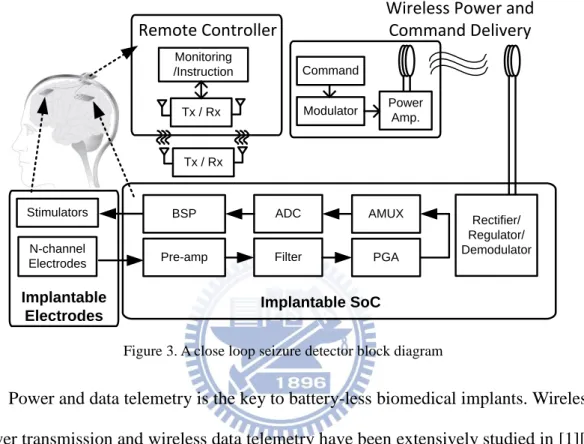
suppression Epilepsy as shown in Figure 3.
Figure 3. A close loop seizure detector block diagram
Power and data telemetry is the key to battery-less biomedical implants. Wireless
power transmission and wireless data telemetry have been extensively studied in [1][2]
and [18]-[27], respectively. In order to transmit command to implants, BER
performance is an important issue but high data rate. Some groups have developed two
pair coils to transmit power and data as shown in Figure 4 and [23]. In order to reduce
the number of implanted coils, systems that transmit both data and power were
proposed in [18][19]. Figure 5 shows the overall data and power transmission system.
The power is transmitted through coils and received inside the human body. The data
demodulator is powered by the rectified power. Pre-amp Implantable SoC Rectifier/ Regulator/ Demodulator Implantable Electrodes BSP Stimulators N-channel Electrodes Filter ADC PGA AMUX Tx / Rx Tx / Rx Monitoring /Instruction Remote Controller Command Modulator Power Amp.
Wireless Power and Command Delivery
Figure 4. Dual coils power and data telemetry
Figure 5. A data and power telemetry
The relation of power efficiency and channel capacity is an issue. The drop-out
voltage of rectifier decides the input peak to peak voltage if a stable DC value is
desired. Power efficiency is calculated by the parameter of coil and internal coil AC
resistance. Once the power consumption of implant circuit is decide, the external
transmitted power is derived. According to the transmission power and coil bandwidth,
capacity is estimated roughly. Detail equations will be introduced in section 3.1.
1.3 Thesis Organization
This thesis covers theoretical analysis of data and power telemetry and practical
circuit design implementation. After introducing the fundamentals of power and data
telemetry, the design challenge of system is discussed. According to the target
specifications of the telemetry, the design procedure from system level to transistor
Power Transmitter Power Recovery Load Data Transmitter Data Recovery NRZ data data Kpwr Kpwr_data1 Kpwr_data2 Kdata External Device Implanted Device Skin carrier Power ampifier Modulator Baseband data Vc1 Vc2 Demodulator baseband data carrier frequency skin internal external VDD GND
level is introduced in detail. The transistor level simulation and prototype chip
measurement are also presented. The thesis is organized as following:
Chapter 1 consists of simple introduction and motivation of this thesis.
Chapter 2 is an overview of general telemetry. The principles of channel capacity
and power efficiency are also described. The fundamental of modulation scheme is
introduced briefly, such as ASK and BPSK. Furthermore, advance techniques of
BPSK demodulator are introduced, which can achieve lower power consumption.
Finally, the related paper is also discussed.
Chapter 3 proposes the system level design procedure. Due to bandwidth of coil,
demodulator must be designed carefully. Power efficiency and channel capacity are
estimated roughly. Finally, a system which connects the coil and demodulator is
simulated by h-spice.
In Chapter 4, practical circuits design and implementation is introduced. Some
non-idealities of practical circuit implementation are considered. The building block
designs of proposed demodulator are detailed. Finally, the transistor level simulation
of BPSK demodulator is presented.
Chapter 5 and Chapter 6 cover the test environment and the experimental result
Chapter 2
Fundamentals of Power and Data Telemetry
_________________________________________
2.1 Relation of Power Efficiency and Channel Capacity
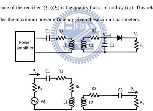
An inductive power link is composed of a transmitter’s and receiver’s coils (L1
and L2), as shown in Figure 6 (a). The coupling coefficient of two coils k (0 < k < 1)
depends on the portion of the total flux lines that cuts both primary and secondary
coils. An AC voltage Vin is applied across the transmitter’s coil, and this induces an
AC voltage Vc1 on the receiver’s coil. Receiving coil is connected to a load Rload
(Figure 6 (a) [4]). Vpeak is a fixed value according to data rate, if rectifier output has to
achieve 1.8 volts. Rectifier input power is defined by equation (1). Therefore, we
estimate the AC resistance by equation (2).
power rec input power=
rectifier efficiency load
R
(1) 2
2 rec input power
peak ac
V
R
(2)The equivalent AC parallel resistance can be transform into equivalent AC series
resistance Figure 6 (b) [4]. The quality factor of the series LC transmitting circuit is
given by 0
1
LC
1 11
L C
2 2
(3) 1 0 1 1Q
L R
,
2 L ac L R R
(4)resistance. Re represents reflected impedance from secondary coil to primary coil.
2 2 1 2 1 2 2 2 2 ac e L acM
R k Q Q
R
R
R
R
R
Q R
(5)A bridge rectifier s used to for convert AC-to-DC conversion. The power
efficiency η between transmitted and received powers (P0 and P1) is represented by
1 2 1 e L o L e
R
R
P
P
R
R
R
R
(6)
2 3 1 2 2 2 2 2 1 2 21
1 2 2 2 o ac ac acP
k Q Q R R
P
R
Q R
k Q Q R
Q R
(7)As shown in Figure 6(b), R2 is the resistance of internal coil and Rac is the input
resistance of the rectifier. Q1 (Q2) is the quality factor of coil L1 (L2). This relationship
provides the maximum power efficiency given these circuit parameters.
Figure 6. Basic circuit for wireless power transmission
This paper presents a scheme that the coils transmit power and data
simultaneously, so we must calculate the system capacity to estimate the limitation of
transmission data rate. However, received power is one of important factors for
determination of the system capacity. This is well known that higher capacity can be
achieved with the higher received signal power.
Power amplifier R1 C1 L1 R2 C2 L2 Vo Ro Vpeak R1 C1 L1 R2 C2 L2 Ro Re Rg Vg Po P1
Figure 7. Basic communication system
According to Figure 7 in this book, as shown in [4], data rate can be discussed by
three part, where are transmitter part, receiver part, and the channel. At first, the
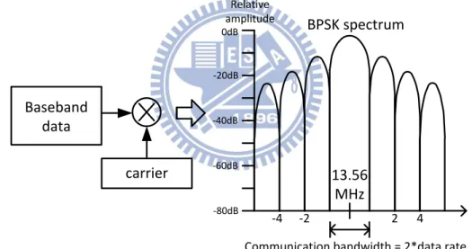
transmitter baseband data rate is half of signal bandwidth, as shown in Figure 8 and
[4].
Figure 8. BPSK modulator and power spectrum
log(1
P
R)
C
B
N
(8) The received power also affects the data transmission. In order to evaluate the
maximum data rate, channel capacity is evaluated, as shown in [10]. Channel capacity
C is impacted by the received signal power PR, LC tank bandwidth B, and noise power N. Considering only thermal noise, the noise power N is given by the Johnson’s
noise formula: (10) information source source encoder channel encoder digital modulation output transducer source decoder channel decoder digital demodulation channel data data Part I Part III Baseband data carrier 13.56 MHz
Communication bandwidth = 2*data rate -2 -4 2 4 BPSK spectrum Relative amplitude 0dB -20dB -40dB -60dB -80dB
(
)
power
N
watts
BKT
(9) where T is the temperature in Kelvin and K is the Boltzmann constant
(1.38×10⁻²³ ). In our simulation, we assume that the system operate at the room
temperature of 27o. The achievable bandwidth B is a function of the Q-factor of
transmitter’s and receiver’s coils [10]. The ratio between signal bandwidth B and carrier frequency f0 is described below. (10)
2 2 2 2 2 2 2 1 2 1 2 1 2 0 1 2
(
)
(
)
4
2
Q
Q
Q
Q
Q Q
B
f
Q Q
(10)The third part is receiver, the receiver’s sensitivity, the sensitivity of an RF
receiver is defined as the minimum signal level that the system can detect with
Acceptable signal-to-noise ratio, as shown in equation (11)-(13) and [6]. SNRin and
SNRout are signal-to-noise ratios measured at the circuit input and output respectively.
Bandwidth is the twice of baseband data rate.
,
sig total RS out
P
P
NF SNR
BW
(11)4
1
174
/
RS S inkT
P
kT
dBm Hz
R
R
(12),min| | / | min|
10log
in dB RS dB Hz dB dB
P
P
NF
SNR
BW
(13)Where Psig,total is received power, PRS is thermal noise, and Pin is the minimum received
power without error. Once the transmitter, channel capacity, and receiver specs are
fixed, we can estimate the highest data rate. The bottleneck of this system data rate will
be the channel capacity, because the transmitter bandwidth is decided by the data rate
we want to transmit, and the receiver bandwidth is wider than channel capacity
because of high received power. There is another issue we have to discuss, the bit error
rate in the communication system. Because the receiver circuit is implanted, we have
correct the data, as shown in equation (14), equation (15) and [4]. The BER is
estimated by the formula which is use for the binary modulation, where fb is bit rate,
and the BW means channel bandwidth:
BW f N E N S b b 0 (14) 2 0 2 0 /2 2 1 0 /2 / 0
1
(
)
2
1
=
2
=Q(
)
b b x N b x N bP n
n
e
dx
N
e
dx
N
(15)2.2 Modulator Scheme Comparison
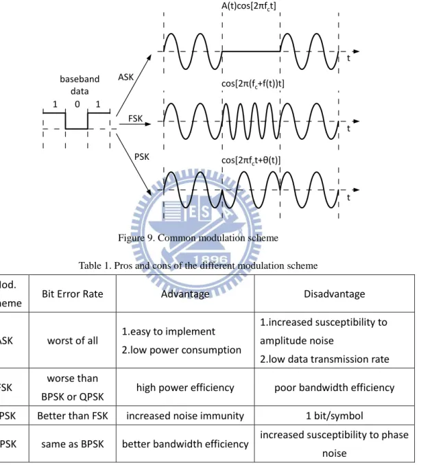
The common used modulation schemes are ASK, FSK and PSK as shown in
Figure 9. ASK modulate the baseband data with the amplitude. One means that the
carrier will be transmitted, zero means that a DC voltage is transmitted. FSK modulate
the baseband data with the frequency. One means that the carrier1 is transmitted, zero
means the carrier2 is transmitted, where the carrier1 and carrier2 is at different
frequency tone. PSK modulate the baseband data with the phase. One means that the 0o
will be transmitted, zero means that the 180o is transmitted. 1 and -1 are the baseband
data, the modulator is like a switch which changes data back and forth. The modulated
data is transmitted by coil operating at the carrier frequency.
Amplitude-shift keying (ASK) or on-off keying (OOK) is frequently used for
data transmission due to its simplicity. However, ASK and OOK modulations suffer
from low data rate and instability for power transmission. In contrast, frequency-shift
keying (FSK) modulation requires a LC resonator with a low quality factor, but this
leads to low power efficiency. Constant-envelope, fixed-carrier frequency
solution for simultaneous data and power transmission. Binary phase-shift keying
(BPSK) is preferred in order to reduce the power consumption of demodulator.
Another advantage of BPSK is that it requires less transmitted power to achieve the
same bit-error rate (BER) when compared to FSK or ASK, as shown in Table 1.
Figure 9. Common modulation scheme
Table 1. Pros and cons of the different modulation scheme
Mod.
scheme Bit Error Rate Advantage Disadvantage ASK worst of all 1.easy to implement
2.low power consumption
1.increased susceptibility to amplitude noise
2.low data transmission rate FSK worse than
BPSK or QPSK high power efficiency poor bandwidth efficiency BPSK Better than FSK increased noise immunity 1 bit/symbol
QPSK same as BPSK better bandwidth efficiency increased susceptibility to phase noise
Figure 10 shows the BPSK modulator [6], the baseband data is modulated by a
switch.For BPSK demodulation, phase-locked loop (PLL) was proposed and it
provides stable data and power transmission [6][7]. However, the high power
consumption of PLL-based demodulator is not suitable for implantable devices since
A(t)cos[2πfct] baseband data 1 0 1 ASK FSK PSK t t t cos[2π(fc+f(t))t] cos[2πfct+θ(t)]
PLL requires phase synchronization for coherent detection. For instance, the most
commonly used squaring or COSTAS loop, as shown in Figure 11 (b). Extracting
clock from received data can be used to eliminate the use of PLL, as shown in Figure
12 (a). This clock-recovery technique was adopted for data transmission [9][10][18],
but applying this technique to simultaneous data and power transmission has not been
explored.
In this work, we propose a clock-recovery-based BPSK demodulator for data and
power telemetry targeting for epilepsy seizure detection. Since power consumption is
an important issue for implantable devices, a symbol edge detector is used instead of a
power-hungry oscillator, as shown in Figure 12 (b). This replacement further reduces
power consumption.
Figure 10. BPSK modulator
Figure 11. (a) Squaring loop (b) Costas loop
XBB(t) +1 -1 +1 -1 Baseband data XBPSK(t) Accos(ωt) Modulated signal XBPSK(t) Baseband data p1(t)=+Accos(ωt) P2(t)=-Accos(ωt) x2 1/2 carrier sin(ωt) data M(t) M (t )s in (ω t) M2(t)sin(ωt) x2 90 M (t )s in (ω t+ Θ1 ) 0 sin(ωt+Θ2) cos(ωt+Θ2) M(t)cos(Θ1-Θ2) M(t)sin(Θ1-Θ2) I Q (a) (b)
comparator clipping
Reset
Generator Clock and Data Recovery Oscillator Data Clock clipping Reset Generator
Clock and Data Recovery
Data Clock comparator Symbol Edge
Detection (a)
(b)
Figure 12. (a) Conventional clock-recovery-based demodulator and (b) proposed oscillator-less demodulator.
2.3 Related Telemetry Paper Review
As we introduce in section 2.2, we prove the theory by the related work. Every
work is used for different telemetry, so data rate and power efficiency demand will be
different. Reference [12][13][14][15] use the ASK modulation, as we can see the
data-to-carrier ratio range is from 0.01 to 0.1. It means that if we transmit 13.56MHz
carrier frequency, the most data rate will be 1.356 Mbps, not mention that these
systems are not take stable power into account. The only one work which transmits
power simultaneously is reference [10]. According the record of this paper, power
varies with the data.
FSK demodulator is introduced in reference [17]. FSK is not use frequently in
power consumption is not mentioned in paper.
BPSK modulation is implemented by reference. Data-to-carrier ratio is from
0.0015 to 1. The reference [18] and [19] successfully transmit a stable 22.5mW to
implant. The reference [22] provides a scheme improving the data-to-carrier ratio to
100%, and the demodulator power consumption is low compared to another scheme,
but this demodulator is not connected to any communication channel.
Table 2. Comparison of the related demodulator
Article Data Transmission Power Transmission
CMOS Tech. (μm) Area (mm2) Mod. , Data rate (Mbps) Carrier freq. (MHz) Power supply (mW) Power consumption (mW) [12] ASK , 1 13.56 136 − 0.35 − [13] ASK , 0.02 2 − 0.815 @ 3.3V 0.35 0.0195 [14] ASK , 2 10 − 0.84 @ 3.3V 0.35 − [15] ASK , 0.3 4 − 1 @ 1.8V 0.18 0.0168 [16] ASK , 2 10 − − 0.35 − [17] FSK , 2 4 or 8 − − 1.5 − [18] BPSK , 1.69 13.56 22.5 5 @ 3.3V 0.5 0.1 [19] BPSK , 1.69 13.56 22.5 2.3 @ 3.3V 0.5 0.293 [20] BPSK , 0.02 13.56 − 3 @ 3.3V 0.5 1 [21] BPSK , 0.8 4 − 0.059 @ 1.8V 0.18 0.0043 [22] BPSK , 0.8 / 4 / 8 / 20 0.8 / 4 / 8 / 20 − 0.046 / 0.093 / 0.148 / 0.31 @ 1.8V 0.18 − [23] DPSK , 2 20 100 6.3 @ 1.8V 0.35 4.42 [24] QPSK , 4 13.56 − 0.75 @ 1.8V 0.18 − [25] QPSK , 8 13.56 − 0.91/0.68 @1.8V 0.18 0.238
The other modulations are DPSK and QPSK respectively. First, we discuss the
DPSK modulation [23], this paper transmit power and data separately (using two coils)
for the optimal power efficiency and data rate. The most important issue of two coils is
cancel the interference by inter-symbol noise subtraction. The other modulation is
QPSK [24][25], as the theory, outstanding data-to-carrier ratio which is high to 0.58,
but the power consumption is much higher than BPSK scheme. According to theory,
the QPSK demodulator is two sets of BPSK basically, so the power consumption of
QPSK will be twice the BPSK using the same circuit.
For a stable power transmission, low demodulator power consumption and high
Chapter 3
System Level Design
_________________________________________
3.1 System Level Parameters
Figure 13 shows the block diagram of this power and data transmission system.
First at all, the coil parameter is defined. Owing to the constraint of implant size, the
inductance of internal coil must be low, where the quality factor of internal coil is low.
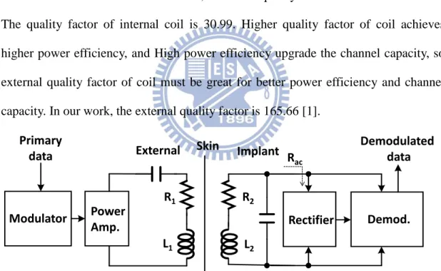
The quality factor of internal coil is 30.99. Higher quality factor of coil achieves
higher power efficiency, and High power efficiency upgrade the channel capacity, so
external quality factor of coil must be great for better power efficiency and channel
capacity. In our work, the external quality factor is 165.66 [1].
Figure 13. A data and power telemetry block diagram
We use a bridge rectifier to convert AC voltage to DC. For the high frequency
(13.56MHz) operation in this power and data telemetry, Schottky diode is chosen to
rectify the received signal. Once the rectifier spec is known, the rectifier efficiency
and the implant circuit power consumption are fixed. In this paper, efficiency of
rectifier achieves 70% based on the datasheet. 5mW is needed for implant circuits. Primary
data
Modulator Power
Amp. Rectifier Demod.
Demodulated data External Skin Implant
R1 R2
Rac
The minimum power received by the inter coil is 7.14mW=5mW/0.7. Rload is rectifier
input resistance parallel with the demodulator input resistance, and input resistance of
the demodulator is high impedance. The input resistance of internal implants is about
Rload. When we measure the coil and rectifier to estimate the power efficiency, demodulator circuit is no need to connect. We want to rectify a 1.8 DC voltage for the
demodulator circuit, and Vpeak of internal coil is 5.8Vpp. Once the internal coil Vpeak
and received power is obtained, the Rac is known to be 2356Ω. The parameter of coil
power efficiency is known, the coupling coefficient is 0.05122, the quality factor of L1
is 165.66, and the quality factor of L1 is 30.99. R2 is 1.05Ω. The power efficiency is
about 26.84%. The external coil has to transmit 26.6mW=7.14mW/0.2684.
Once the received signal is obtained, the channel capacity could be estimated.
We know that the C=Blog(1+S/N). The channel bandwidth B is 78kHz which is
calculated by equation. The S is the received power 7.14mW. The N=BW*K*T. In our
simulation we have assumed that the system is operating at the room temperature of
about 27o in the resonance frequency 13.56MHz. If the communication bandwidth is
varied with data rate, N=828*data rate*10-17. We assume that the data bandwidth is 1
Mbps. Then the channel capacity is estimated to 942.9 kbps. After the SNR is known,
the BER is estimated as well. Eb/N0=(SNR*(channel bandwidth))/bit rate.
Eb/N0=6.81*1010 (BER < 10-9).
3.2 Coil and Rectifier Architecture
Once the implant physical size constraint is decided by system application, the coupling coefficient(k) can be maximize by proper choosing the outer diameter size of coils, and the Q factor can be maximize by the coils’ structure and coils’ material. Since Q factor and coupling coefficient are increase as the outer diameter increase, the first step of efficient near-field coils design maximizing the coupling coefficient would not conflict
the design parameter of maximizing the Q factor. Once we maximize the coupling coefficient by deciding the primary and outer diameter of secondary coil, that recent research have been widely studied [34], we can maximize the Q factor by using allowable wide copper metal and low loss coil structure. The coil structure mainly divides into three parts: multi-layer cylindrical coil, single layer cylindrical coil and spiral coil, as shown in Figure 14 (c). The different structure have different Q factor, because the skin effect and
the proximity effect [35]. In this paper, the single layer cylindrical coil is used for external coil because the greater quality factor. The internal coil which we choose is the spiral coil, because the cylindrical coil is too thick to implant.
Figure 14. (a) Single layer cylindrical coil (b) Multi-layer cylindrical coil (c) Spiral coil which is winded by copper conductor
The carrier resonance frequency is set to 13.56MHz.The parameters of coils are
summarized in Table 3.
Table 3. External and internal coil spec
Primary coil Secondary coil
L (μH) 7 0.382 C (pF) 18.8 374.25 R (Ω) 3.6 1.05 Q 165.66 30.99 diameter (cm) 4.2 1.1 thickness(cm) 1.8 0.2
After coil parameters are fixed, the rectifier spec is known. We use simple bridge
rectifier by using schottky diode, as shown in Figure 15 (a). When the positive cycle
r
r
(b) (c)
is applied to the rectifier (the solid line), D1 and D3 is conducting, and the D2 and D4
are cut off. The induced current in internal coil goes through the red path, as shown in
Figure 15 (b). When the negative cycle is applied to the rectifier (the solid line), D2
and D4 is conducting, and the D1 and D3 are cut off. The induced current in internal
coil goes through the red path, as shown in Figure 15 (c).
Figure 15. (a) Bridge rectifier (b) Positive cycle function of the bridge rectifier (c) Negative cycle function of the bridge rectifier
Once the rectifier function is working, we let that the rectifier conducting voltage
be Vr. DC voltage applied to the Rload is that Vpeak minus 2Vr as shown in Figure 16.
Rload is input resistance of VDD and GND in demodulator which is 1.2kΩ. We connect a large capacitor 1μF to make the ripple of Vo as small as we can.
If we transmit all 0 or all 1 data (a 13.56 MHz sine wave without modulated), we
can derive the rectified DC value by the equation (16)-(19) and Figure 16.
2 O S V V V (16) D1 D2 D3 D4 Rload Rload Rload (a) (b) (c)
min exp 2 O p T V V RC (17) _ , 2 2 3 4 3 r pp p p r p V T T V V V V RC RC (18) _ 1 2 2 r pp O p p V T V V V RC (19)
Figure 16. (a) Relation of rectifier drop-out voltage and input Vpeak (b) Ripple of Vr
3.3 BPSK Demodulator Architecture
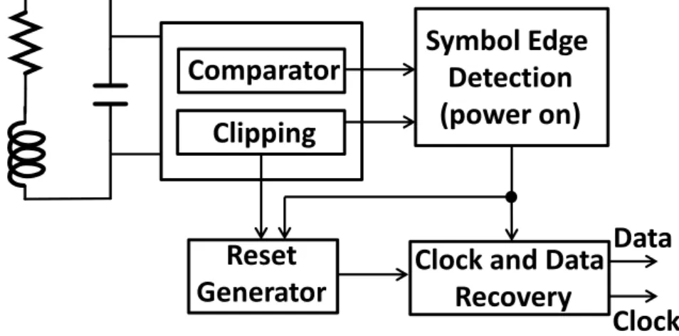
A clock-recovery-based demodulator architecture is adopted to reduce the
complexity induced by PLL. The BPSK demodulator circuit is presented in Figure 17.
There are four blocks, and the first block of comparator and clipping which is
connected to internal coil. The second block is enable circuit, and it’s an important
part to power on at the symbol edge. The third block is reset generator which is used
for generating the right reset signal at inter-symbol. The last block is data and clock
recovery, where is used to regenerate the baseband data and carrier frequency.
Figure 17. A BPSK demodulator block diagram in this work
T/2 T 2T Vo Vs 2Vr V t (a) T 2T Vo V t (b) Vp t
Symbol Edge
Detection
(power on)
Clipping
Comparator
Reset
Generator
Clock and Data
Recovery
Data
Clock
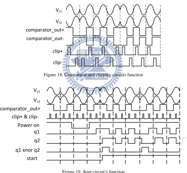
Figure 18 shows waveform of first block. BPSK modulation converts baseband
data 0 and 1 into two in-phase waveforms. It converts analog signals to digital signals
through comparator and clipping circuit. When the Vc1 > 0 and Vc2 < 0, the
comparator_out+ is high and comparator_out- is low. When Vc1 > 1.05V, the
clip_out+ is high and clip_out- is low. When the Vc2 > 0 and Vc1 < 0, the
comparator_out- is high and comparator_out+ is low. When Vc2 > 1.05V, the clip_out-
is high and clip_out+ is low. Once these four signals are obtained, the later circuit will
start by detecting these signals.
Figure 18. Comparator and clipping circuits function
Figure 19. Start circuit’s function
The right symbol edge should be detected in order to recover the data. There are
two circuits to generate the enable signal. The first is a circuit named start circuit, one
of the differential outputs of the clipping circuit (clip+ or clip-) is used to extract the
clock frequency and trigger the start signal. Figure 19 shows the functionality of the Vc1 Vc2 comparator_out+ comparator_out-clip+ clip-Vc1 Vc2 comparator_out+ clip+ &
clip-Power on q1 q2 q1 xnor q2 start
start circuit. An external power on signal is switched to enable the detection process.
The second circuit is named enable circuit. Because the start circuit is triggered at the
clip_out edge, which will make the enable signal is leading for a half cycle. We use a
3-bit counter which counts to 7 to start the enable signal as shown in Figure 20. The
counter counts to 7, so the signal is triggered leading for a half cycle also. The final
enable signal is triggered at symbol edge correctly.
Figure 20. Enable circuit’s function
The third block is the reset generator, as shown in Figure 21. After digital signals
are extracted, there is an edge detection circuit to detect rising or falling edges. When
two falling edges are detected, the reset signal is pulled to high. The reset signal goes
down if a rising edge is detected. The reset generator is working until the enable
signal is pulled to low.
Figure 21. Reset circuit’s function
Vc1 Vc2 comparator_out+ start q0 q1 q2 enable Vc1 Vc2 comparator_out+ clip+ clip-enable reset
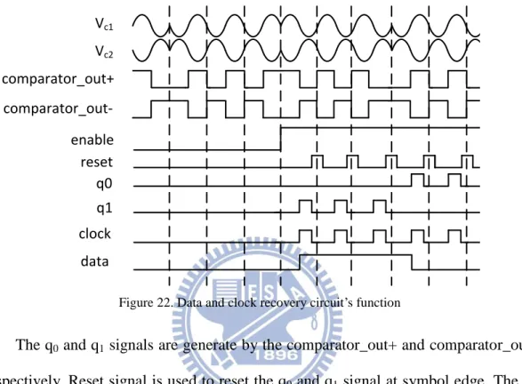
We propose an area-efficient circuit implementation for data-and-clock recovery
(DCR). It consists of two D flip-flops whose clocks come from the differential outputs
of the comparator and data input is connected to high. Timing diagram of the key
signals are shown in Figure 22.
Figure 22. Data and clock recovery circuit’s function
The q0 and q1 signals are generate by the comparator_out+ and comparator_out-
respectively. Reset signal is used to reset the q0 and q1 signal at symbol edge. The q0
and q1 generate a clock. Frequency of this clock is the same as carrier from the coil.
Once the reset signal goes high, an edge detector generates right signals to DCR.
3.4 System Level Simulation
We simulation the coil and demodulator circuit simultaneously by h-spice. If we
transmit the same power to the external coil, the received coil amplitude changes with
different data rate as shown in Figure 23. The last line is the received waveform at
13.56 Mbps data rate, and it’s clearly that the power is not transmitted to the internal
at all. Figure 23 shows that the data rate higher than channel capacity. It’s clearly that
the received input waveform’s distortion is too large to detect by our BPSK
demodulator. We estimate that comparator_out+ is wrong at every symbol edge. The Vc1 Vc2 comparator_out+ enable reset comparator_out-q0 q1 clock data
data is impossible to be recovery.
Figure 23. Received waveform in internal coil at data rate higher than 678 kbps with PRBS
Primary data Vin Vc1 Primary data Vin Vc1 Primary data Vin Vc1 Primary data Vin Vc1 13.56 Mbps 1.356 Mbps 452 kbps 135.6 kbps 0 1u 2u 3u 4u 5u 6u 7u 8u
Chapter 4
Circuit Design and Implementation
_________________________________________
4.1 Comparator and Clipping Circuit
As introduced in Chapter 3, we have to digitize the modulated signals. In the
beginning, comparator and clipping circuits are needed. The most important issue of
comparator and clipping circuit is to make sure that the transitions of these two
circuits occur on different input voltage.
A common mode DC voltage in the comparator circuit is 0 volt. We assume that
the differential input varies from -4 volt to 4 volt. In this part, we separate the DC and
transient analysis into 4 regions, as shown in Figure 25 (a).
Figure 24. (a) Transient analysis of comparator (b) Direct current analysis of comparator
Region I: when Vc1 = -4 volts and V c2 = 4 volts, |VsgM1| > |Vthp| and |VsgM1- Vthp |
> |Vsd|. M1 is operating in saturation region. M2, M3 and M4 are in cut off region.
The point V1 is at high level, and V2 pulls to low, as shown in Figure 25 (b). I II III IV
V
c1 -4 -4 -3 -3 -2 -2 -1 -1 0 0 1 1 2 2 3 3 4 4 VOLTS(volt) (lin) -4 4 v(vc1) -4 4 v(vc2) -700u -300u0 i(mx1) -700u 0 i(mx2) 100u 700u i(mx3) 100u 700u i(mx4) 0.2 1 1.8 v(1) 0.2 1 1.8 v(2)Region II: When V c1 decreases and Vc2 increases, as |VsgM2| > |Vthp| and |VsgM2-
Vthp | < |Vsd|, M2 is going to operate at triode region. Once current of M2 is not 0 volt,
V2 and VdsM4 increaseto conduct M4. When |VgsM3| < |Vthn|, M3 is still in cut off
region, as shown in Figure 25 (c).
Region III: When V2 continues to increase, as |VgsM3| > |Vthn|, M3 is operating at
triode region. Once V1 decreases simultaneously, as |VgsM4| < |Vthn|, M4 is in cut off
region, as shown in Figure 25 (d) .
Region IV: When V c1 still increases, as |VsgM1| < |Vthp|, M1 is cut off, and current
of M3 is 0 volt. We can derive that V1 is at 0 volt and V2 is at 1.8 volt, as shown in
Figure 25 (e).
Figure 25. States of the comparator (a) comparator circuit (b) region I (c) region II (d) region III (e) region IV M1 M2 M3 M4 Vc1 Vc2 comparator_out+ 1 2 comparator_out-M1 M2 M3 M4 Vc1 Vc2 1 2 0 1.8 M1 M2 M3 M4 Vc1 Vc2 1 2 0 1.8 M1 M2 M3 M4 Vc1 Vc2 1 2 0 1.8 M1 M2 M3 M4 Vc1 Vc2 1 2 0 1.8
(a)
(b)
(c)
(d)
(e)
The other circuit is clipping. According to chapter 3, we know that the output
spec of clipping and comparator. Clipping pulls differential output to high when input
signal is larger than 1 volt, as shown in Figure 26. We separate the transient and DC
analysis into 5 regions, as shown in Figure 27 (a).
Region I: when V c1 = -4 volt and V c2 = 4 volt, as |VsgM1| > |Vthp| and |VsgM1- Vthp |
>|Vsd|, M1 is operating at saturation region. When |VsgM2| < |Vthp|, M2 is cut off.
Current of M4 and M6 are zero. When V2 is 0 volt, we can derive that |VgsM3| < |Vthn|.
|VgsM5| is smaller than |Vthn|, as shown in Figure 27 (b).
Region II: When V c1 increases and V c2 decreases, as |VsgM2| > |Vthp|, M2 is at
triode region. However, V2 is still too low to make M4 and M6 to operate in triode
region, as shown in Figure 27 (c).
Region III: In this region, V2 is still larger than 2 Vthn. M3 and M5 is operating at
saturation region. We can see that M1 to M6 are at saturation region. V1 and V2 are
1.8 volt right now. If we connect a small size inverter to V1 and V2, clipping
differential outputs will be 0 volt at the same time, as shown in Figure 27 (d).
Figure 26. (a) Transient analysis of clipping (b) Direct current analysis of clipping
Region IV: Once Vc1 increase and Vc2 decrease, M1 is going to operate in triode
region. With the decreasing current of M1, V1 will be smaller than 2 Vthn. M4 and M6 I II III IV V IV III
V
c1 -4 -3 -2 -1 0 1 2 3 4 VOLTS(volt) (lin) -4 4 v(vc1) -4 4 v(vc2) -30u 0 i(mx1) -30u 0 i(mx2) 5u 30u i(mx3) 5u 30u i(mx4) 5u 30u i(mx5) 5u 30u i(mx6) 0.2 1.8 v(1) 0.2 1.8 v(2) -4 -3 -2 -1 0 1 2 3 4are in cut off region, as shown in Figure 27 (e).
Region V: In final region, VsgM2= VDD-V c1. When |VsgM2| < |Vthp|, M1 is cut off.
V1 is at 0 volt and V2 is at 1.8 volt, as shown in Figure 27 (f).
Figure 27. States of the clipping (a) clipping circuit (b) region I (c) region II (d) region III (e) region IV (f) region V
4.2
Power and Data Distinguish
This paper shows the telemetry which transmits power and data simultaneously,
so it’s important to distinguish the power and data. When the data is prepared to
deliver, we must sure that the signal which starts the whole demodulator circuit will
be triggered at symbol edge. First, there is a start circuit which uses two DFFs to
ensure the correctness of start signal. If a transition of data occurs, comparator
M1 M2 M3 M4 Vc1 Vc2 clip+ clip-1 2 M1 M2 M3 M 4 Vc1 Vc2 clip+ clip-0 1.8 M1 M2 M3 M4 Vc1 Vc2 clip+ clip-0 1.8 M1 M2 M3 M4 Vc1 Vc2 clip+ clip-1.8 1.8 M1 M2 M3 M4 Vc1 Vc2 clip+ clip-0 1.8 M1 M2 M3 M4 Vc1 Vc2 clip+ clip-1.8 0
(a)
(b)
(c)
(d)
(d)
(e)
M5 M6 M5 M6 M5 M6 M5 M6 M5 M6 M5 M6positive end output will be zero or one for a cycle as shown in Figure 28.
Figure 28. Waveform of received analog signal and comparator output
The input of the first stage DFF is comparator single end output named
comparator_out+. Power on signal which is triggered by user will be the reset input of
these two DFFs, as shown in Figure 29. The second stage output will delay half cycle
compared to first stage. Once data transition occurs, the output of these DFFs will be
the same (all 0 or all 1). We use a XOR gate and an inverter to detect the transition. A
signal where q0 XNOR q1 is obtained, it will be a clock of the last DFF. Once the
DFF is triggered, the start will be high until the power on signal reset it.
Figure 29. Start circuit in this work
After start signal is triggered, a 3-bit counter is used to enable the data
demodulator. The enable signal is given by power on circuit, as shown in Figure 30.
Once we start to transmit data, the counter counts to 7 to enable the whole
demodulator circuit. The initial value of this counter is reset to zero by and gate and
XOR gate. Once the counter counts to 7. q0、q1and q2 are all high, at this time, if power on signal is low, the XOR gate output will be low. The initial value is set.
1 0 0 1 0 Baseband data Received signal Comparator_out+ Q Q SET CLR S R RST Q Q SET CLR D RST SET Comparator_out+ Q Q SET CLR S R RST Q Q SET CLR D RST SET Q Q SET CLR S R RST Q Q SET CLR D RST SET Power on clip+ &
Figure 30. Enable circuit in this work
These DFF clock signal are comparator output. In this section, transmit bit data
which is zero, it means that the first half cycle of comparator output is 1.8 volt, and
the last half cycle is 0 volt. If we transmit data one, the output will be opposite to zero.
One thing is sure that the start signal is triggered at symbol edge. As we can see
(Figure 31), if DFF is positive triggered, the start signal will be right when data is one,
but it will be error when data is zero. We have to use two sets counter to fixed it, one
counter is positive edge triggered, and another one is triggered by negative edge. The
two counters input are comparator_out+ and comparator_out- separately. The enable
signal will be trigger at symbol edge, as shown in Figure 32.
Figure 31. Waveform of positive triggered enable circuit
Figure 32. Waveform of positive and negative triggered enable circuit
4.3
Reset Generator
Q Q SET CLR S R RST Q Q SET CLR D RST SET Q Q SET CLR S RRST Q Q SET CLR D RST SET Q Q SET CLR S RRST Q Q SET CLR D RST SET Comparator_out+ Reset Start Enable Initial data 0 Initial data 1 0 0 Start Enable Comparator_out+ Initial data 1 Initial data 1 0 0 Start Enable Comparator_out+After the enable signal is triggered, the reset generator starts to work. It’s
important to produce a reset signal at symbol edge. A cycle of received data will
output one clip+ and clip- signals no matter the data is one or zero. The circuit detects
two falling edge of clip+ and clip-, and it means one cycle is received, and then the
rest signal is pulled to high. Inter symbol transitions will be reset.
We use two DFFs to divide frequency of clip+ and clip-. The enable pulls to high
at symbol edge, but the clip+ and clip- signal have a little delay. We assume that the
clock (clip+ and clip-) will trigger after delay compared to enable as shown in Figure
33 and Figure 34. We separate the flow to four parts.
Part I: When enable is low, DFF is set to be high using set=1 and reset=0.
Part II: When enable is high, but the clip+ and clip- is not going to high yet. At
this time, enable exclusive or Q will be zero.
Part III: clip+ or clip- pulls to high, DFF will pass value zero from D to Q, and it
will make the enable exclusive or Q signal become one. Then the state will be keeping
until the next positive edge trigger.
Part IV: the clock trigger again, the D value one will pass to Q.
D is twice period of clock as shown in Figure 34. The signal which is enable
exclusive or Q becomes zero. And the D value will be zero.
Part III and Part IV will be a loop until the enable become low again.
Figure 33. DFF cell of reset circuit Q Q SET CLR S R RST Q Q SET CLR D RST SET Clock Enable Enable Clock
Figure 34. DFF function of the reset circuit
The whole reset generator circuit shows in Figure 35. The upper DFF is used to
detect the rising edge. And the lower DFF is used for falling edge detecting. The
lower DFF clock input will be opposite to the upper DFF.
After we obtained the str and stf signals, as shown in Figure 36. We can use these
two signals to construct the signal we want. We know that these two signals will be
high simultaneously at one symbol end to the start of the next symbol. We can
successfully produce a reset signal, as shown in Figure 36.
Figure 35. Reset circuit in this work
enable 0 0 0 1 1 1 1 1 1 1 1 1
clock 1 1 0 0 1 1 0 0 1 1 0 0
D 1 1 1 0 1 1 1 1 0 0 0 0
Q 1 1 1 1 0 0 0 0 1 1 1 1
set D=1 one cycle one cycle
t Q Q SET CLR S R RST Q Q SET CLR D RST SET Q Q SET CLR S R RST Q Q SET CLR D RST SET Enable Clip+ Clip-Stf Str Reset
Figure 36. Waveforms of the reset circuit
4.4
Data and Clock Recovery
A data and clock recovery system is introduced here, as shown in Figure 37. First,
we want to get the clock signal. The data input D of these two DFFs are high, and the
clock input will be comparator differential output respectively. The reset signal is
generated by the reset circuit. If data which we transmit is one, the upper DFF output
q_bar will be pull to low when the positive edge occurs, and q_bar will pull to high
when reset signal is high. If data which we transmit is zero, the lower DFF is working
like the upper one. After the q1_bar and q2_bar are obtained, a NAND gate is used to
recover a periodic clock. The clock frequency will be the same as carrier frequency.
At last, baseband data must be generated. The last stage DFF data input is Q1. If data
is one, the first half cycle of symbol is low, and after the half cycle is high. If data is
zero, the whole cycle is low. When the last DFF clock is triggered at the later cycle of
symbol, data is obtained. enable ~(clip+ & clip-)
clip+ & clip-str
stf reset
Figure 37. Data and clock recovery circuit in this work
4.5
Transistor Level Simulation
We use radio-frequency h-spice to simulate our BPSK demodulator. In this
section, we show the simulation results of each part which we mention in 4.1 to 4.4.
At first, transistor size of comparator and clipping circuits are showed in Figure 38.
We have to sure that the common mode DC value of these two circuits. When input
Vc1 and Vc2 common mode DC is ground, the comparator differential output 0 and 1
transition will occur at 133mV which is near to 0 volt, as shown in Figure 39 (a).
Table 4 shows the input offset versus the comparator and clipping transition. If the
input offset is higher than 0.6 volts, the comparator and clipping output transition will
be at the same input voltage. This situation will make the later circuit malfunction.
Figure 38. Comparator and clipping circuit with transistor size Q Q SET CLR D Q Q SET CLR S R Q Q SET CLR S R RST RST RST Comparator_out+ Comparator_out+ Reset Clock Data SET Q Q SET CLR D RST SET Q Q SET CLR D RST SET M1 M2 M3 M4 Vc1 Vc2 comparator_out+ comparator_out-1 2 M1 M2 M3 M4 Vc1 Vc2 clip+ clip-1 2 12.2/0.37 1.5/0.2 7/0.35 m=5 0.3/0.2 0.3/0.2 (a) (b) M5 M6
Figure 39. (a) Pre-simulation waveforms of comparator and clipping DC analysis at 0V offset (b) 0.6 V offset
Table 4. DC offset versus comparator and clipping transition voltage
offset (V) comparatot_out+(mV) comparatot_out- (mV) clip+ (V) clip- (V)
0 0.133 0.133 1.05 -1.06
0.6 1.11 1.11 1.11 -0.126
After the comparator and clipping circuit is determined, we have to ensure that
the later circuit delay is smaller than our function limitation. There are four states
-4 -4 -3 -3 -2 -2 -1 -1 0 0 1 1 2 2 3 3 4 4 v1(volt) (lin) -4 -2 0 24 v(vc1) -4 -2 0 24 v(vc2) 0.2 0.6 1.2 1.8 v(comparator_out+) 0.2 0.6 1.2 1.8 v(comparator_out-) 0.2 0.6 1.2 1.8 v(vclip_bf+) 0.2 0.6 1.2 1.8 v(vclip_bf-) (a) -3 -3 -2 -2 -1 -1 0 0 1 1 2 2 3 3 4 4 v1(volt) (lin) -2 0 2 4 v(vc1) -3 -2 0 2 4 v(vc2) 0.2 0.6 1.2 1.8 v(comparator_out+) 0.2 0.6 1.2 1.8 v(comparator_out-) 0.2 0.6 1.2 1.8 v(vclip_bf+) 0.2 0.6 1.2 1.8 v(vclip_bf-) (b)
when we transmit data. They were one to zero、zero to zero、zero to one and one to
one.
Case I: Symbol edge at transition of data from 1 to 1 is shown in Figure 40 (a).
The enable circuit delay from comparator output to enable is less than 1.04ns. As we
can see that the clip- is 4.3ns far from comparator output. The enable will be triggered
before the transition of clip+. The reset generator circuit latency is less than 0.425ns.
The comparator output transition is 3ns from clip+. So the reset signal is working at
the right time here. Once the enable and reset signal are ready, data and clock will be
right.
Case II: Symbol edge at transition of data from 0 to 0 is shown in Figure 40 (b).
The enable circuit delay is less than 1.02ns. The clip- is 4.6ns far from comparator
output. Enable is triggered before the transition of clip+. The reset generator circuit
latency is less than 0.425ns. The comparator output transition is 0.8ns from clip+.
Reset signal is working at the right time here. Once the enable and reset signal are
ready, data and clock will be right.
Case III: Symbol edge at transition of data from 0 to 1 is shown in Figure 40 (c).
Start circuit’s latency is 0.64ns. The enable circuit delay is less than 1.04ns. The clip-
transition is 7.4ns far from clip+ transition. The enable will be triggered after the
transition of clip-. Correctness of the reset generator circuit is sure. Reset generator
circuit output will be wrong if the comparator transition is complete before clipping
transition, but the comparator transition won’t happen in this case. So the reset signal
is always right. Once the enable and reset signal are ready, data and clock will be
right.
Case IV: Symbol edge at transition of data from 1 to 0 is shown in Figure 40 (d).
transition is 7ns from clip+ transition. Enable is triggered after the transition of clip-.
It is sure that the correctness of the reset generator circuit. The reset generator circuit
output will be wrong if the comparator transition is complete before clipping
transition, but the comparator transition won’t happen in this case. Reset signal is
always right. Once the enable and reset signal are ready, data and clock will be right.
Figure 41 shows that the transient simulation of comparator and clipping output.
Once the data transition occurs, one end of clipping differential output is low, and the
other end has two pulses. One end of comparator differential output is high, and the
other end is high.
Figure 40. (a) Transition of data from 1 to 1 (b) Transition of data from 0 to 0 (c) Transition of data from 0 to 1 (d) Transition of data from 1 to 0
14.9u 14.92u 14.94u 14.96u 14.98u 15u 15.02u 15.04u
TIME(sec) (lin) v(vc1) v(vc2) v(comparator_out+) v(comparator_out-) v(vclip_bf+) v(vclip_bf-)
15.06u 15.08u 15.1u 15.12u 15.14u 15.16u 15.18u
(a) (b) TIME(sec) (lin) -4 -2 0 2 4 -4 -2 2 4 0.8 1.4 1.8 0 0.8 1.4 1.8 0.2 0.6 1.2 1.8 0.2 0.6 1.2 1.8 0 -4 -2 0 24 -4 -2 2 4 0.8 1.4 1.8 0 0.8 1.4 1.8 0.2 0.6 1.2 1.8 0.2 0.6 1.2 1.8 0
14.98u 15u 15.02u15.04u 15.06u15.08u 15.1u 15.12u 15.86u 15.88u 15.9u 15.92u 15.94u 15.96u 15.98u 16u
TIME(sec) (lin) v(vc1) v(vc2) v(comparator_out+) v(comparator_out-) v(vclip_bf+) v(vclip_bf-) (c) (d) -4 -2 0 2 4 -4 -2 2 4 0.2 0.8 1.4 1.8 0 0.8 1.4 1.8 0.2 0.6 1.2 1.8 0.2 0.6 1.2 1.8 0 -4 -2 0 2 4 -4 -2 2 4 0.8 1.4 1.8 0 0.8 1.4 1.8 0.2 0.6 1.2 1.8 0.2 0.6 1.2 1.8 0 TIME(sec) (lin)
Figure 41. Pre-simulation waveforms of differential input, comparator and clipping output
At the beginning, we simulate the delay between power on signal and start signal.
As we introduce in 4.2, when the power on is triggered by user, the start signal is
triggered at the data transition (0 to 1 or 1 to 0). Table 5 shows the gate delay of this
circuit. When the data is from zero to one, we can know that the start signal pulls to
high after 0.64ns delay from clip+ and clip-. Figure 42 (a) shows the simulation
waveform. When the data is from one to zero, we can know that the start signal pulls
to high after 0.6ns delay from clip+ and clip-. Figure 42 (b) shows the simulation
waveform.
Table 5. Delay of the start circuit with data from 1 to 0 or 0 to 1
Data=1-0 Data=0-1
input output rise_delay (ns) input output rise_delay (ns)
clip start 0.64 clip start 0.6
13.5u 14u 14.5u 15u
TIME(sec) (lin) -4 -2 0 2 4 v(vc1) -4 -2 0 2 4 v(vc2) 0 0.4 0.8 1.4 1.8 v(comparator_out+) 0 0.4 0.81 1.4 1.8 v(comparator_out-) 0 0.4 0.8 1.4 1.8 v(vclip_bf+) 0 0.4 1 1.4 1.8 v(vclip_bf-)