國立交通大學
電子工程學系 電子研究所
碩 士 論 文
三維積體電路關鍵技術
於先進背照式感光元件應用之研究
Key Technologies of 3-D ICs for Advanced BSI-CIS
Application
研 究 生:呂典融
指導教授:陳冠能 博士
三維積體電路關鍵技術
於先進背照式感光元件應用之研究
Key Technologies of 3-D ICs for Advanced BSI-CIS
Application
研 究 生:呂典融
Student: Dian-Rong Lyu
指導教授:陳冠能 博士
Advisor: Prof. Kuan-Neng Chen
國立交通大學
電子工程學系 電子研究所
碩士論文
A Thesis
Submitted to Department of Electronics Engineering & Institute of Electronics College of Electrical & Computer Engineering
National Chiao Tung University in Partial Fulfillment of the Requirements
for the Degree of Master
in
Electronics Engineering & Institute of Electronics November 2013
Hsinchu, Taiwan, Republic of China
三維積體電路關鍵技術
於先進背照式感光元件應用之研究
研究生:呂典融 指導教授:陳冠能 博士 國立交通大學 電子工程學系 電子研究所碩士班摘 要
背面照射互補示電晶體影像感應元件為下一世代的感光影像元件,相較於傳統 的前面照射元件,背面照射有許多好處,像是減少雜訊、降低楊氏干涉現象、 增加感光亮以及減少色彩的失真…等等。在現今的背面照射互補示電晶體影像 感應元件的製程中大多會使用銅錫凸塊和點膠(underfill)兩種技術。銅錫凸塊被 用來做為晶片和基板之間的電性連接,並且搭配點膠技術來提升其整體的可靠 度。然而,由於銅錫凸塊接合技術在微縮上的困難,以至於限制了整個晶片的 微縮。在本篇論文中提出縮減銅鎳錫接合的厚度,以達到次微米級的應用,並 且配合其他三維積體電路關鍵技術:金屬接合及晶圓薄化技術,完成背面照射互 補式電晶體影像感應元件的測試結構。為了確保在電性上的可靠度,我們在銅 i錫對銅錫凸塊的接合上進行克爾文測試結構(Kelvin test structure)及凸塊鏈接 (daisy chain)的電性分析。而傳統的點膠,可能會在銅錫凸塊間留下許多的空洞 及孔隙,在之後的可靠度測試中會造成相當程度的問題。因此,我們利用三維 積體電路中的混合接合技術,使用其中的高分子部份取代了點膠,以解決點膠 不完全所造成的可靠度問題。因此先研究其中的高分子接合作為前導研究,並 以聚醯亞胺(polyimide, PI) 當作主要材料,研究聚醯亞胺的基本性質,並且利 用材料分析和一連串的拉力及切割測試找出適合的接合條件並探討其機制。 ii
Key Technologies of 3-D ICs for Advanced BSI-CIS
Application
Student: Dian-Rong Lyu Advisor: Prof. Kuan-Neng Chen
Department of Electronics Engineering & Institute of Electronics National Chiao Tung University
Abstract
Backside illumination CMOS image sensor (BSI-CIS) has many advantages such as
reducing the noise beyond low illumination to lighten color distortion, enhancing the
sensor current, and lowering the effect of Young's interference. Cu/Sn to Cu/Sn bump
with under-fill is proposed to use in BSI-CIS fabrication. However, current Cu/Sn bump
and under-fill technologies limit the scaling of the CIS chip. In this thesis, we reduce
the Cu/Sn thickness successfully by novel Cu/Ni/Sn bonding and fabricate the test
structure of BSI-CIS by wafer thinning and wafer bonding technologies. In addition,
we evaluate the correspodning electrical characteristics and reliabilities in Kelvin test
structure and daisy chain. On the other hand, during the under-fill filling, there are some
issues like the micro-gap or voids between the Cu/Sn bumps. The concept of hybrid
bonding can be used to solve these problems. In order to study the feasibility of hybrid
bonding by Cu/Ni/Sn and polymer, we first evaluate polyimide dielectric bonding under
different bonding temperature, and study the correlation between different parameters
such as curing, time and temperature by FTIR. We also investigate the mechanical
properties by pulling test and dicing test. These results of Cu/Ni/Sn bonding and
polyimide bonding have provided the guideline for using hybrid bonding in BSI-CIS
applications.
誌謝
研究所的過程中,最感謝當然就是指導我的陳冠能老師,在老師充滿美式 風格的帶領之下,3DIC Lab 總是跟其他實驗室不同,永遠充滿了笑聲,除此之 外,在研究上,老師也總是不遺餘力的支持我們在實驗室的研究,因為陳冠能 老師的細心指導,讓我在研究所的生涯中學到很多很多,在實驗之外,老師也 教導了其他東西,不斷提醒著我們應該有的態度和作事情的方法。除了老師之 外,也感謝實驗室的大家,一起奮鬥的小予、妤珊和若寧,跟你們一起做實 驗、一起八卦、一起桌遊,真是這兩年內非常重要的一部分,耀仁學長和星翰 學長不厭其煩的跟我討論實驗,在我整個實驗中扮演了相當重要的角色,彥斌 學長、珽崵學長、建宇學長、毓宸學長、世偉學長以及荃安學長,在我煩悶的 時候,能給我適時的鼓勵及幫助,也感謝各位學弟妹,能幫我處理許多實驗室 的事,讓我能夠專心的在研究上。 室友俊宏、晨明、順盛,雖然我們都在不同的領域,但彼此卻能互相打 氣、互相體諒,真是非常得開心,如果我有什麼做不好的地方,也請你們多多 包涵了。也相當感謝單單、美蘭、鐿瀞、群群和旂豪,認識你們是我在碩士生 涯中一段重要的意外,和你們當室友的日子裡,T-building 總是充滿了笑聲, 一起看電視一起大笑,而在難過時,我們也能一起打氣一起走過,就像一家人 一樣,在我最後的碩士生活裡,真的非常謝謝你們。 感謝口試委員鄭晃忠老師、侯拓宏老師,在口試時給予的建議及指導,並 讓我的口試順利結束。最後,最重要的感謝就是我的父母了,因為有你們,所 以我才能無後顧之憂的在研究上,順利完成碩士學位。 v 電子工程學系 電子研究所碩士班 國立交通大學Contents
摘 要... i Abstract ... iii 誌謝... v Contents ... vi List of Tables ... ix List of Figures ... x Chapter 1 Introduction ... 1 1.1 Background ... 1 1.2 Motivation ... 41.3 Organization of the Thesis ... 6
Chapter 2 Experimental Instruments ... 12
2.1 Introduction ... 12
2.2 Process Instruments ... 13
2.2.1 Oxford Plasma Enhanced Chemical Vapor Deposition System... 13
2.2.2 Sputter ... 14
2.2.3 Flip Chip Bonder... 15
2.2.4 EVG520HE ... 16
2.3 Material Analysis Instruments ... 17
2.3.1 Scanning Electron Microscopy Hitachi S-4700I ... 17
2.3.2 Scanning Acoustic Tomography ... 18
2.3.3 Fourier-Transform Infrared Spectrometer... 18
2.4 Electrical Analysis Instrument ... 21
2.4.1 4156C ... 21
2.5 Reliability Test Instrument ... 22
2.5.1 Pulling Force Tester 1220S ... 22
Chapter 3 Reliability Investigation on Cu/Sn to Cu/Sn Bump Bonding ... 30
3.1 Introduction ... 30
3.2 Experimental Procedure ... 31
3.3 Results and Discussion ... 32
3.3.1 Contact Resistance Measurements ... 32
3.3.2 Daisy Chain Measurements ... 32
3.3.3 Current Cycling Test ... 33
3.3.4 Thermal Cycling Test ... 33
Chapter 4 Investigation on Cu/Ni/Sn Bonding and Wafer Thinning Applied on Fabrication of BSI-CIS ... 40
4.1 Introduction ... 40
4.2 Fabrication of BSI-CIS Testing Structure ... 42
4.3 Results and Discussion ... 43
4.3.1 Wafer Bonding ... 43
4.3.2 Wafer Thinning and Stop Layer Selection ... 43
Chapter 5 Investigation of Polymer Bonding with Polyimide ... 55
5.1 Introduction ... 55
5.2 Experimental Procedure ... 57
5.3 Results and Discussion ... 58
5.3.1 Material Analysis ... 58
5.3.2 Chip-Level Polyimide Bonding with High Temperature Curing . 59 5.3.3 Polyimide Bonding with Low Temperature Curing ... 60
Chapter 6 Conclusion and Future Work ... 73
6.1 Conclusion ... 73
6.2 Future Work ... 75
References ... 76
List of Tables
Chapter 1 Introduction
Table 1-1 Classification of 3D IC Processes and Integration Techniques ... 11
Chapter 3 Reliability Investigation on Cu/Sn to Cu/Sn Bump
Bonding
Table 3-1 Resistance of the Daisy Chain ... 36
Chapter 4 Investigation on Cu/Ni/Sn Bonding and Wafer Thinning
Applied on Fabrication of BSI-CIS
Table 4-1 The Etching Rate of KOH ... 50 Table 4-2 Etch Rate of TMAH ... 52
Chapter 5 Investigation of Polymer Bonding with Polyimide
Table 5-1 Cure Condition of Different Temperature ... 64 Table 5-2 SAT Image of Polyimide Bonding Cured at 300 °C ... 65 Table 5-3 SAT Image of Polyimide Bonding Cured at 320 °C ... 65 Table 5-4 SEM Image of Polyimide Bonding Cured at 200°C, 30 min and
320°C, 60min ... 68 Table 5-5 Polyimide Bonding at Low Temperature Curing and Bonding ... 68 Table 5-6 Pulling Test with Different Curing and Bonding Temperature .... 68 Table 5-7 Results of Polyimide Bonding with Two Steps Curing ... 72 Table 5-8 Results of Polyimide Bonding with One Step Curing ... 72
List of Figures
Chapter 1 Introduction
Figure 1-1 Roadmap of Semiconductor ... 7
Figure 1-2 Concept and Fabrication of 3DIC [2]... 7
Figure 1-3 3D-IC Technology Integrate Different Function Chips by Heterogeneous Stack ... 8
Figure 1-4 Development of 3D IC Scheme ... 8
Figure 1-5 Comparison between FSI-CIS and BSI-CIS ... 9
Figure 1-6 Comparison between (a) C4 Solder Interconnect and (b) Low-Volume Lead-Free Solder Interconnect [4] ... 9
Figure 1-7 Hybrid Bonding Chip ... 10
Chapter 2 Experimental Instruments
Figure 2-1 Outlook of Plasma Enhanced Chemical Vapor Deposition ... 23Figure 2-2 Outlook of Sputter ... 23
Figure 2-3 Outlook of Flip Chip Bonder ... 24
Figure 2-4 Illustration of Different Alignment Methods [9] ... 25
Figure 2-5 Outlook of EVG 520 ... 26
Figure 2-6 Outlook of Scanning Electron Microscopy ... 26
Figure 2-7 Outlook of Scanning Acoustic Tomography (SAT) ... 27
Figure 2-8 Range of FTIR Measurement [10] ... 27
Figure 2-9 Outlook of Fourier-Transform Infrared Spectrometer ... 28
Figure 2-10 Four-probe measurement system ... 28
Figure 2-11 Setup before the Tensile Test and Samples after the Curing in the Tester before the Tensile Test ... 29
Figure 2-12 Outlook of Pulling Force Tester 1220S ... 29
Chapter 3 Reliability Investigation on Cu/Sn to Cu/Sn Bump
Bonding
Figure 3-1 (a) Cross Section (b) Measurement of Kelvin Structure ... 34Figure 3-2 (a) Cross Section (b) Measurement of Daisy Chain ... 34
Figure 3-3 Specific Contact Resistance of Kelvin Structure with Cu/Sn Bump Bonded ... 35
Figure 3-4 Equivalent Circuit in Our Structure ... 35
Figure 3-5 Resistance of Daisy Chain ... 36
Figure 3-6 AC Current Stressing of Daisy Chain (-0.1 A to 0.1 A) ... 37
Figure 3-7 AC Current Stressing of Kelvin Strucutre (-0.1 A to 0.1 A) ... 37
Figure 3-8 Contact Resistance after Thermal Cycling Test ... 38
Figure 3-9 Specific Contact Resistance of Thermal Cycling Test ... 38
Figure 3-10 Resistance of Daisy Chain of Thermal Cycling Test with 20 Bumps ... 39
Chapter 4 Investigation on Cu/Ni/Sn Bonding and Wafer Thinning
Applied on Fabrication of BSI-CIS
Figure 4-1 Process of BSI CIS Testing Structure proposed by ITRI ... 47Figure 4-2 Process of BSI CIS Testing Structure ... 47
Figure 4-3 SAT Analysis of Blanket Wafer Bonding Result... 48
Figure 4-4 SAT Analysis of Blanket Wafer Bonding Result... 48
Figure 4-5 SEM Images of Cu/Ni/Sn to Cu/Ni/Sn Bonded at 250 °C for 30min ... 49 Figure 4-6 SEM Images of Cu/Ni/Sn to Cu/Ni/Sn Bonded with 1 μm Poly
Silicon at 250 °C for 30min ... 49
Figure 4-7 The SEM Image of Etching Procedure ... 50
Figure 4-8 Morphology of Wafer after 49% HF Etching ... 51
Figure 4-9 Morphological Measurement of P-10 after 49% HF Etching .... 51
Figure 4-10 The SEM Image of Etching Procedure ... 52
Figure 4-11 (a) Grinded Wafer with 10μm Residual Substrate (b) Removed the Substrate after the TMAH Etching (c) Stop Layer Removed ... 53
Figure 4-12 Wafer of BSI-CIS Testing Structure ... 53
Figure 4-13 Morphology by AFM (a) Standard Silicon Wafer (b) Wafer of BSI-CIS Testing Structure ... 54
Chapter 5 Investigation of Polymer Bonding with Polyimide
Figure 5-1 Dianhydride and Diamine [23-24] ... 62Figure 5-2 Molecule of Polyamic Acid [24] ... 62
Figure 5-3 Chemical Formula of Polyimide Formation [25] ... 62
Figure 5-4 FTIR Analysis of Polyimide [26] ... 63
Figure 5-5 Symmetrical C=O Bond Formation [26]... 63
Figure 5-6 Polyimide Structure ... 63
Figure 5-7 FTIR of Curing at Different Temperature ... 64
Figure 5-8 SEM Image of Polyimide Bonding at 200 °C ... 66
Figure 5-9 SEM Image of Polyimide Bonding at 250 °C ... 66
Figure 5-10 SEM Image of Polyimide Bonding at 200 °C ... 67
Figure 5-11 SEM Image of Polyimide Bonding at 250 °C ... 67
Figure 5-12 SEM Image of Polyimide Bonding at 300°C and 350°C ... 67
Figure 5-13 Polyimide Bonding with Two Wafer Cured at 150°C for 90 min ... 69
Figure 5-14 Dicing Test of Polyimide Bonding with Two Wafer Cured at 150°C for 90 min (a) bonded at 150°C (b) bonded at 250°C ... 69 Figure 5-15 Polyimide Bonding with Two Wafer Cured at 200°C for 90 min
... 70 Figure 5-16 Dicing Test of Polyimide Bonding with Two Wafer Cured at
200°C for 90 min (a) bonded at 150°C (b) bonded at 200°C (c) bonded at 250°C ... 70 Figure 5-17 Polyimide Bonding with Two Wafer Cured at 250°C for 90 min
... 71 Figure 5-18 Dicing Test of Polyimide Bonding with Two Wafer Cured at
250°C for 90 min (a) bonded at 150°C (b) bonded at 200°C (c) bonded at 250°C ... 71
Chapter 1
Introduction
1.1
Background
With the development of semiconductor industry, the chip functionalities are
enhanced by scaling down the transistors. However, scaling cannot keep going.
Due to the lithography and physical limitations, the scaling technology will meet
the bottleneck in the future [1]. To overcome the challenges and improve the chip
performance, the three-dimensional integrated circuits (3DIC) is one of the
promising solutions. The roadmap of semiconductor by Fairchild (Figure 1-1)
indicates 3D IC can extend Moore’s Law and keep the semiconductor product
toward the high-density, high performance, short wiring, and low power
consumption (Figure 1-2) [2]. Therefore, 3D IC is very important for
semiconductor industry.
Three-dimensional integration is an advanced approach using several mixed
technologies including through silicon via (TSV), wafer bonding and chip stacking,
wafer thinning, wafer handling, etc. Wafer bonding and chip stacking are common
methods for stacking various devices (Figure 1-3), and then, through–silicon via
(TSV) connects the thinning wafers and chips to accomplish integrated
heterogeneous applications. It can transform the traditional 2D IC to 3D IC and
the development is shown in Figure 1-4.
In spite of advantages of stacking, thermal budget of each process should be
focused to ensure 3D IC working normally. Chip fabrication includes many
different processes. The temperature of the later process needs to be lower than
the former one so that degradation of devices’ performance can be avoided because
of high temperature. Therefore, the bonding temperature is a critical issue, which
restricts many transistor applications like the waveguide transistors and the
integration of traditional CMOS [3]. But now these problems can be resolved by
optimized design of the chip bonding, and the heterogeneous integration of 3D IC
can meet future demands.
Due to its attracting merits, 3D IC technology will subvert traditional 2D IC.
And it is closely linked to IC design, process techniques, instruments, packaging,
testing methods, terminal product application and performance. In addition, 3D IC
involves using different substrate materials, bonding materials and stuffing
materials. Many derivative phenomena of material and physics need to be resolved.
Under many kinds of process selections, developing 3D IC with low cost, high
yield and high performance is the key point.
With the development of 3D IC technologies, the 3D IC technologies are
applied to CMOS image sensor and MEMS now. The CMOS image sensor (CIS)
is an attracting technology to apply for mobile application. The type of CMOS
sensor is divided into front-side illumination CMOS image sensor (FSI-CIS) and
backside illumination CMOS image sensor (BSI-CIS). The differences between
FSI-CIS and BSI-CIS are the metal wiring and photo diode, which are shown in
the Figure 1-5. For FSI-CIS, light transmits into the front side of the IC and passes
through metal wiring before the photo diode. For FSI-CIS, in contrast, light
transmits into the back side of the IC and passes through photo diode before the
metal wiring with BIS-CIS. The advantages of BIS-CIS are reducing the noise
signal beyond low illumination and lightening color distortion, enhancing the
sensor sensitivity, lowering the effect of Young's interference, etc. The 3D IC
technology is important for fabricating the BSI-CIS. It can scale down the chip
size, enhance the performance and so on.
1.2
Motivation
The advanced CMOS image sensor (CIS) is an important device for mobile
application while recent studies of cell phone point out some drawbacks of common
front-side illumination CMOS image sensor including large light noise, low
symmetric aperture, low incident light dose and large pixel area. To solve the
problems mentioned above, we cooperate with ITRI to develop backside
illumination CMOS image sensor (BSI-CIS) using advanced three-dimensional
integrated circuits technology in this work. In our part, we propose the design
method and provide key technologies of 3D IC and ITRI fabricate it by using their
novel equipment. Finally, we measure the fundamental electrical properties of
simplified test structure.
However, the process of BIS-CIS cooperated with ITRI has to use Cu/Sn bump
and under-fill. The Cu/Sn bump bonding has been widely used in mass production
but it needs a larger spacing between bumps [4]. The spacing between bumps limits
the scaling of the whole chip. To reach the application of sub-micron scale, reducing
the Cu/Sn thickness is important and necessary (Figure 1-6). On the other hand,
during the under-fill filling, some problems like the micro-gap and voids between
the Cu/Sn bumps are needed to overcome. The hybrid bonding can be used to solve
the problems [5-7]. It has the ability to combine metal bonding with oxide or
adhesive, such as BCB, SU-8 and polyimide (Figure 1-7), which is able to achieve
native metal interconnection with adhesive isolation. Because the adhesive is used
to play the role of bonding material and under-fill filling, it effectively improves the
bonding strength. The most important thing is that the electrical interconnect and
inner-gap filling can be fabricated at the same time [8]. Thus, the process flow can
be simplified and avoid the micro-gap filling change.
The purposes of the study reported here are (a) the investigation of the
electrical characteristics and reliabilities of Cu/Sn to Cu/Sn bump bonding (b)
reducing the Cu/Sn thickness and accomplishing the BSI-CIS testing structure
with metal bonding and wafer thinning (c) the polyimide bonding conditions and
its corresponding mechanism.
1.3
Organization of the Thesis
In Chapter 2, the major characteristics of all instruments which are used in
this thesis will be literally introduced.
In Chapter 3, we measure the Cu/Sn to Cu/Sn bump bonding electrical
characteristics including Kelvin structure and daisy chain. In addition, we also
work on the reliability tests about current stressing and thermal cycling test.
In Chapter 4, we develop the procedure to do Cu/Ni/Sn bonding and wafer
thinning.
In Chapter 5, after the studies of Cu/Ni/Sn bonding and wafer thinning, we
investigate the polymer bonding. The property of polyimide, various bonding
conditions and bonding mechanism are included in this thesis.
In Chapter 6, we will give a conclusion for this thesis and some suggestions.
The future work for this study will be mentioned as well.
(Fairchild)
Figure 1-1 Roadmap of Semiconductor
Figure 1-2 Concept and Fabrication of 3DIC [2]
(Zycube, MNCN)
Figure 1-3 3D-IC Technology Integrate Different Function Chips by
Heterogeneous Stack
(Yole Développement, 2007)
Figure 1-4 Development of 3D IC Scheme
(Sony, 2008)
Figure 1-5 Comparison between FSI-CIS and BSI-CIS
Figure 1-6 Comparison between (a) C4 Solder Interconnect and (b)
Low-Volume Lead-Free Solder Interconnect [4]
Figure 1-7 Hybrid Bonding Chip
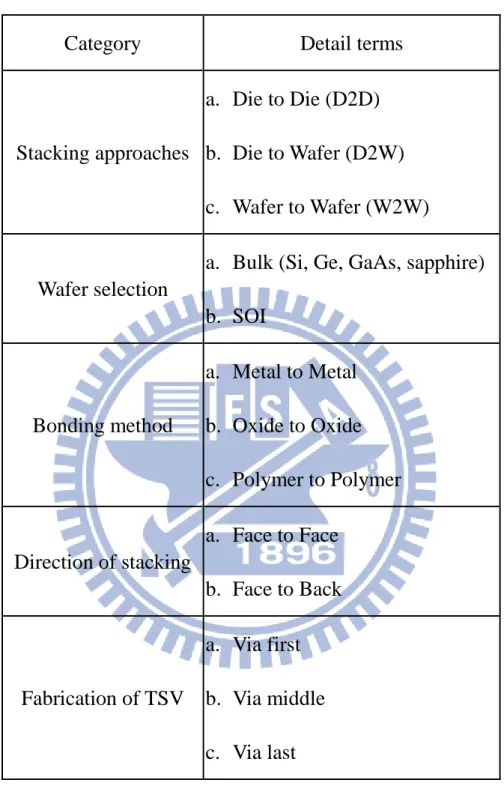
Table 1-1 Classification of 3D IC Processes and Integration Techniques
Category
Detail terms
Stacking approaches
a. Die to Die (D2D)
b. Die to Wafer (D2W)
c. Wafer to Wafer (W2W)
Wafer selection
a. Bulk (Si, Ge, GaAs, sapphire)
b. SOI
Bonding method
a. Metal to Metal
b. Oxide to Oxide
c. Polymer to Polymer
Direction of stacking
a. Face to Face
b. Face to Back
Fabrication of TSV
a. Via first
b. Via middle
c. Via last
11Chapter 2
Experimental Instruments
2.1
Introduction
In this chapter, some of the equipment instruments are been described. They
play an important role in our research. It is divided into three parts: process
instruments, material analysis instruments and reliability test instrument.
All the samples studied in this work are prepared in Nano Facility Center
(NFC), Center for Nanotechnology, Materials Science, and Microsystems
(CNMM) and National Nano Device Laboratories (NDL).
The material analysis conducts in Material Analysis Technology (MA-tek),
Integrated Service Technology (iST) and Center of Nanoscience and Technology
in NCTU. Material analysis and microscope instruments are used to let us
understand the related and the corresponding properties of the process condition.
Scanning electron microscopy (SEM), scanning acoustic tomography (SAT) and
the Fourier-transform infrared spectrometer (FTIR) are used. All the instruments
will be introduced as follows.
2.2
Process Instruments
2.2.1 Oxford Plasma Enhanced Chemical Vapor Deposition
System
Plasma enhanced chemical vapor deposition (PECVD) is usually used for the
thin film deposition, and make material source change from gas state into plasma
state to accelerate chemical reactions. The outlook of PECVD shows at Figure 2-1.
The plasma is filled by process gases and generated by two electrodes which are
biased with RF signal or DC signal. Processing plasmas are usually operated at the
pressures of a few mTorr to a few Torr, so the atoms and ions can reach enough
mean free path. Ionized atoms or molecules are accelerated towards or leave the
neighboring surface in sheath region (depends on their charges); therefore, all
surfaces exposed to the plasma receive ion bombardment. The potential across the
sheath layer is typically 10–20 V. The sheath layer is naturally generated because
those electrons move faster than atoms or molecules, and can produce much higher
sheath potential by modified reactor geometry. Ion bombardment leads to
increases in density of the film and removes contaminants that cover the sample
surface to improve the film quality. Ion bombardment density can be high enough
to do thin film planarization. Silicon dioxide can be deposited by using different
silicon precursor gasses like dichlorosilane or silane and oxygen precursors.
Silicon nitride can be formed by using silane and nitrogen or ammonia. Silicon
dioxide can also be deposited from a tetra-ethyl-ortho-silicate (TEOS) silicon
precursor in oxygen or oxygen-argon plasma. Silicon dioxide deposited by
high-density plasma can create a nearly hydrogen-free film with good conformity.
2.2.2 Sputter
Ion Tech Microvac 450CB was used for depositing metal materials. The
outlook of sputter shows at Figure 2-2.The sputtering system is composed of: (1)
Sputtering chamber (2) vacuum pumps, consisting of one cryo pump and
mechanical pump (3) DC power (4) 4-inch magnetron gun (5) gas flow meter (6)
pressure gauges (7) film thickness monitor. The 4-inch or 6-inch Si substrates are
placed in the spin holder driven by a motor. The targets (metals such as Cu, Ti,
Fe, etc.) are 4-inch. The DC source can provide power up to 200 W. Normally
the base pressure is around 3.0 × 10⁻⁶ torr and the working pressure is around 7.6
mtorr. The flow rate of Ar is around 24 sccm. The sputtering DC source is kept at
160W for our experiments.
Its basic principle is physical vapor deposition. PVD is driven by
momentum exchange between the ions and atoms in the materials. The incident
ions set off collision cascades in the target. When such cascades recoil and reach
the target surface with energy higher than the surface binding energy, an atom
can be ejected out of the target surface.
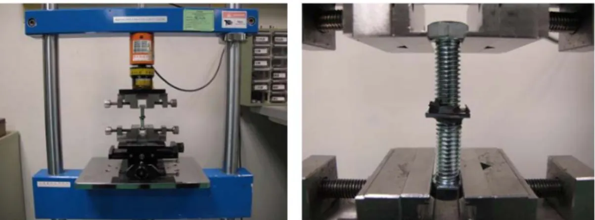
2.2.3 Flip Chip Bonder
This multipurpose bonding platform FINEPLACER Pico MA for advanced
assembly can process bonding step with 5 μm accuracy shown at Figure 2-3. And it has high magnification to do alignment procedure. Advanced device packaging
like assembly of MEMS, sensors, RFID, embedded components and surface
mount photonics can be completed with this bonder. Also, it can execute precise
die attach, flip chip bonding, LED bonding and chip to wafer (6”) bonding. Some
high technologies have been adopted on this instrument such as thermo
compression, thermo sonic, ultrasonic bonding, soldering (AuSn, C4, Indium),
face-up/face-down assembly, flip chip on flex, chip on glass (CoG) and adhesive
technologies (ACF/ACP/NCP). Some features are spotlighted like vision
alignment system ensures placement accuracy within 5μm, larger field of view and working area (6”), shifting module for bigger chip sizes, quick and easy setup of
new applications, manual & motorized configuration available, hands-off
operation in motorized configuration, high resolution video optics with fiber optic
lighting, process observation and monitoring and independent substrate handling
without tool change. Its software “WinFlipChip” can do advanced process
recording and reporting functions, control of all connected process modules,
advanced force control, drag & drop function to adjust profiles, options to capture
pictures and graphical user interface. The picture and schematic of the bonder are
shown in Figure 2-3 and Figure 2-4 [9].
The alignment method of this bonder is type 3 inter-substrate microscopes,
with two set of microscopes capturing the image of top and bottom bonding samples.
The spec of the bonder is as follows:
Placement accuracy 5 μm
Components from 0.125 mm × 0.125 mm to 100 mm × 100 mm
Working area up to 450 mm × 234 mm
Supporting wafer/substrate sizes up to 8"
Supporting bonding force up to 100 N
Can be configured as a hot air rework system
Manual and semi-automatic configurations
2.2.4 EVG520HE
The EVG520HE is a thermo-compression bonding tool shown at Figure 2-5;
the theory of thermo-compress bonding is using pressure and heat to make the
contact area between these two wafers distort slightly to increase contact area. At
a certain temperature that is high enough at the wafer surface, these wafers will
diffuse between each other to make the bonding process complete. This method
does not require strict surface cleaning and high vacuum condition.
Because thermo-compression bonding process is simpler and less cost, it is
more attractive to industry and academic circle. The most important parameter in
this method is temperature. Wafer level bonding is used at 3D-IC device and
application, so the bonding temperature should be compatible with BEOL
(back-end-of-line) to avoid influencing device performance and reliability.
EVG520HE is a single chamber tool that the maximum size of processed
wafer is 4 inch. Besides, it can handle 2 × 2 cm2 chip. It is a semi-automatic tool
that can heat or cool upper and bottom wafer at the same time. And EVG520HE
has individual ramp system to provide different process temperature to upper and
bottom wafer. The maximum process temperature is 350℃, besides, it can
provide compression force up to 12000Nt for 4 inch wafer to enhance bonding
and does not require vacuum environment to do bonding process.
2.3
Material Analysis Instruments
2.3.1 Scanning Electron Microscopy Hitachi S-4700I
SEM provides a convenient way to inspect the surface morphology and the
cross section image of the critical layer. The outlook of SEM shows at Figure 2-6.
We need to coat a thin Pt layer on the samples to enhance conductivity and get a
high quality image before sending the samples into the chamber. The accelerated
electron beam is emitted from a cold-cathode electron gun with the extract voltage
ranging from 0.5 kV to 30 kV. The electron will collide with DUT, and the
secondary electrons originate within a few nanometers from the surface of the
DTU. The electrons are detected and rendered into a bright SEM image.
2.3.2 Scanning Acoustic Tomography
SAT is the abbreviation of Scanning Acoustic Tomography and it is also
called SAM (Scanning Acoustic Microscope) shown at Figure 2-7. The SAT
examinations were performed at frequency above 20 kHz, with a point to point
resolution of 10 nm. The principle of detection of SAT is transmitting the
ultrasonic to the sample, and analyzing the reflection and transmission of
ultrasonic with software. By the software, we can check the line and layer inside
the chip that cannot be seen by naked eye. In the SAT image, the dark region
indicates good bonding interface without voids, whereas the white region
represents the bonding interface with voids. During the SAT examination, the
sample was placed in the water because the ultrasonic is very sensitive to air.
2.3.3 Fourier-Transform Infrared Spectrometer
When the molecular vibration occurs in the atoms, it will absorb a specific
energy, which will form IR spectrum. Unlike the ultraviolet or visible light, the
IR cannot cause electronic transitions. The absorption of IR radiation would be
limited in the molecule generally (Figure 2-8) [10]. Since each vibration or
rotation of molecules has special energy, the specific wavelength will be
absorbed. So we can understand the molecular structure by the IR spectrum.
We can use the interferometer to produce interference wave irradiated the
samples, and then we can get the interference spectrum by Fourier transform.
The advantage is the measurement speed and sensitivity are more accurate and
higher resolution. The FTIR can detect the wafer, film, liquid and solid sample
and the FTIR spectrum can be divided into three types including reflection,
transmission and absorption. In the three types of spectrum, the reflection
spectrum can be divided into attenuated total reflection (ATR), diffuse reflection
(DRIFT), 75° grazing incident angle reflectance and specular reflection (SR).
The FTIR consists of five units: optics module, electronic unit, water cooling
unit, vacuum system and PC data station. The picture and schematic of the FTIR
are shown in Figure 2-9
The spec of the FTIR is as follows:
Range of measurement: 500~700 1/cm (1.43~20.00 μm) Sample size: 8 mm × 8 mm~20 mm × 20 mm
Sample thickness: < 10 mm
At first, we need to measure the background sample before we measure the
sample and let the spectrum of sample divided by the spectrum of background
sample, and then we can get the spectrum. The FTIR can only detect the relative
intensity, which it is not the quantity analysis.
2.4
Electrical Analysis Instrument
2.4.1 4156C
Agilent 4156C precision semiconductor analyzer is used to measure the
electrical properties of the bonded structure. The 4156C provides highly accurate
laboratory bench top parameter analyzers for advanced device characterization.
The superior low-current and low-voltage resolution and built-in quasi-static CV
measurement capability of the 4156C provide a firm foundation for future
expansion with other measurement instruments, as shown in Figure 2-10.
The 4284A precision LCR meter is a cost-effective solution for component
and material measurement. The wide 20 Hz to 1 MHz test frequency range and
superior test-signal performance allow the 4284A to test components to the most
commonly-used test standards, such as IEC/MIL standards, and under conditions
that simulate the intended application. Whether in research and development,
production, quality assurance, or incoming inspection, the 4284A will meet all of
your LCR meter test and measurement requirements.
2.5
Reliability Test Instrument
2.5.1 Pulling Force Tester 1220S
The Pulling Force Tester 1220S are used to measure the tensile. In this
work, it is used to measure the bonding strength. Before the tensile test, the
sample was stick to screw by thermosetting resin adhesive at 150℃ for 2 h as
shown in Figure 2-11.
After the curing, the sample was set in the auto inserting pulling force
tester. The picture and schematic of the pulling force tester are in Figure 2-12
The spec of the pulling force tester is as follows:
Maximum measurement: 175 kgf
Sample size: 1.5 cm × 1.5 cm
(National Nano Device Laboratories)
Figure 2-1 Outlook of Plasma Enhanced Chemical Vapor Deposition
(Nano Facility Center)
Figure 2-2 Outlook of Sputter
(Fine Tech)
Figure 2-3
Outlook of Flip Chip Bonder
Figure 2-4 Illustration of Different Alignment Methods [9]
(Center for Nanotechnology, Materials Science, and Microsystems)
Figure 2-5 Outlook of EVG 520
(The University of California Riverside)
Figure 2-6 Outlook of Scanning Electron Microscopy
(Hitachi FS300II, Japen)
Figure 2-7 Outlook of Scanning Acoustic Tomography (SAT)
Figure 2-8 Range of FTIR Measurement [10]
(Center of Nanoscience and Technology)
Figure 2-9 Outlook of Fourier-Transform Infrared Spectrometer
Figure 2-10 Four-probe measurement system
Figure 2-11 Setup before the Tensile Test and Samples after the Curing in
the Tester before the Tensile Test
(SE TESTSYSTEMS CO, Taiwan)
Figure 2-12 Outlook of Pulling Force Tester 1220S
Chapter 3
Reliability Investigation on
Cu/Sn to Cu/Sn Bump Bonding
3.1
Introduction
Cu/Sn to Cu/Sn bump bonded interconnect is an important technology [13],
which can be used in flip chip packaging process. It plays the role of connecting the
image sensor and substrate, so the reliability is very important. In order to verify
the capability of Cu/Sn to Cu/Sn bump bonded interconnect for commercial use and
mass production, reliability investigation on Cu/Sn to Cu/Sn is strongly required.
In this chapter, the daisy chain and Kelvin structure of the Cu/Sn to Cu/Sn
bump bonded interconnect was designed to verify electrical characterization and
reliability assessment including: contact resistance measurement, AC current
stressing test and thermal cycling test. Four-probe Agilent 4156C analyzer was
adopted for electrical measurement. The electrical characteristics of the 3D
integration scheme were evaluated through the bond chain structures, where a series
of Cu/Sn bumps was included.
3.2
Experimental Procedure
In the integration scheme, daisy chain and Kelvin structures were designed in
the test vehicle for investigation. Kelvin structure is a design to investigate the
electrical property of contact resistance. Figure 3-1 (a) shows the cross section of
Kelvin structure. Figure 3-1 (b) shows the measurement of Kelvin structure. Figure
3-1 (c) is the Kelvin structure. Daisy chain is a design to evaluate the stability of
series number of bumps. Figure 3-2 (a) shows the cross section of daisy chain.
Figure 3-2 (b) shows the measurement of daisy chain. Figure 3-2 (c) is the daisy
chain. To avoid loading effect on SMU and cable line, the method was modified
and measured in four-probe SMU system. One current injection and outflow
another SMU and then we measure delta V between two pads.
To evaluate the stability of bonded structure and electrical performance, the
current cycling test was performed and the current sweeping range was -0.1 A to
0.1 A. To evaluate the thermal reliability of bonded structures, a temperature cycling
test ranging from -55 °C to 125 °C was conducted and the demonstrations of the
test were based on the JEDEC standard.
The resistance values of the samples were measured by 4-point measurement
with Kelvin structure. The current stressing tests and thermal cycling tests were
conducted on the Cu/Sn to Cu/Sn samples.
3.3
Results and Discussion
3.3.1 Contact Resistance Measurements
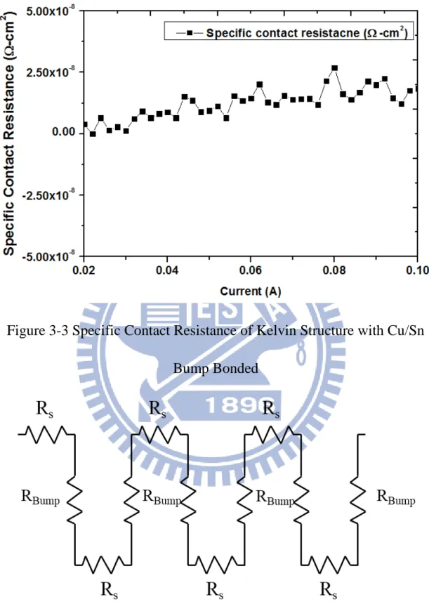
The contact resistance of Cu/Sn bump bonded interconnect was evaluated by
fabricating and measuring a Kelvin structure of a bonding area subjected to 1960
μm2. We calculate the specific contact resistance of the bonded structure with the
following equation:
ρ
c= R
c× A
c(1)
In the equation (1),
ρ
c is specific contact resistance, Rcis contact resistance
and Acis contact area. In this work, the specific contact resistance
ρ
cis 1.24 ×
10-8 Ω-cm2, the result is shown in Figure 3-3.3.3.2 Daisy Chain Measurements
Daisy chain is used for evaluating the stability of series number of bumps.
We measured the number of bumps: 0, 12 and 20. The resistance without bumps
shows the resistance of the metal line, which can be used to remove the loading
effect. As the Figure 3-4 illustrated, the resistance without bumps is Rs. In the
Table 3-1, the Rs is 1.78 Ω, the resistance with 12 bumps is 0.44 Ω, and the
resistance with 20 bumps is 0.7 Ω. So we can know the resistance of a bump is about 0.35 Ω. The result of measurement is shown in Figure 3-5.
3.3.3 Current Cycling Test
The stability of the bonding is significant for 3D integration applications,
especially its electrical performance after multiple operations. Therefore, the
current cycling tests of Cu/Sn bump bonded interconnect were evaluated. The
AC current stressing test for 1000 cycle was applied to the Cu/Sn bump, with
each cycling consisting of a current sweeping from -0.1 A to 0.1 A. The result of
daisy chain is shown in Figure 3-6, and the result of Kelvin structure is shown in
Figure 3-7. The result implies that the bonded structure is stable and it can also
endure a long term electrical current.
3.3.4 Thermal Cycling Test
To evaluate the thermal reliability of bonded structures, a temperature
cycling test for 1000 cycles and 2000 cycles was conducted. The test condition
are ranging from -55 °C to 125 °C and ramp rate is 15 °C/min. The results of
Kelvin structure were shown in Figure 3-8, and the specific contact resistances
were shown in Figure 3-9. The resistance after thermal cycling test is more stable
than initial. The results of daisy chain are shown in Figure 3-10, the resistance
decreases from 2.48 Ω to 2.38 Ω. It may come from the improvement of bonded interface, like the grain growth and removal of defects.
Figure 3-1 (a) Cross Section (b) Measurement of Kelvin Structure
(c) Structure of Kelvin Structure
Figure 3-2 (a) Cross Section (b) Measurement of Daisy Chain
(c) Structure of Daisy Chain
Figure 3-3 Specific Contact Resistance of Kelvin Structure with Cu/Sn
Bump Bonded
Figure 3-4 Equivalent Circuit in Our Structure
Figure 3-5 Resistance of Daisy Chain
Table 3-1 Resistance of the Daisy Chain
Number of bumps 0 12 20 Resistance (ohm) 1.78 2.22 2.48
Figure 3-6 AC Current Stressing of Daisy Chain (-0.1 A to 0.1 A)
Figure 3-7 AC Current Stressing of Kelvin Strucutre (-0.1 A to 0.1 A)
37Figure 3-8 Contact Resistance after Thermal Cycling Test
Figure 3-9 Specific Contact Resistance of Thermal Cycling Test
38Figure 3-10 Resistance of Daisy Chain of Thermal Cycling Test with 20
Bumps
Chapter 4
Investigation on Cu/Ni/Sn
Bonding and Wafer Thinning
Applied on Fabrication of
BSI-CIS
4.1
Introduction
The BSI-CIS is the next generation image sensor since it has many
advantages compare to front side illumination CMOS image sensor (FSI-CIS)
[11-12], like reducing the noise signal beyond low illumination to lighten color
distortion, enhancing the sensor current, lowering the effect of Young's
interference so that the sensor can further scale down and so on. However,
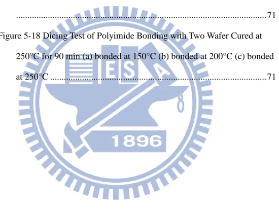
process proposed by ITRI has to use the Cu/Sn bump, handling wafer and
under-fill, which is shown in Figure 4-1. In addition, the Cu/Sn to Cu/Sn bump bonded
interconnect has been widely used in package process. It needs a larger spacing
between bumps. The spacing between bumps limits the scaling of the whole
chip. To reach the application of sub-micron scale, reducing the Cu/Sn thickness
is necessary and important.
In this chapter, we design a new process flow of BSI-CIS. We use Cu/Ni/Sn
to Cu/Ni/Sn bonding to accomplish the BSI-CIS testing structure with metal
bonding and wafer thinning. In addition, we don’t use handling wafer in the
whole process, the bonded substrate can be served as a support to avoid wafer
bow, warpage and so on. Scanning electron microscope (SEM) was applied for
the image and the Scanning Acoustic Tomography was used to inspect the
bonding area uniformity.
4.2
Fabrication of BSI-CIS Testing Structure
P-type (100) 4-inch Si wafers were adopted in the study. The silicon dioxide
with 3000 Å were deposited on bare silicon wafers after RCA clean (SPM + SC1
+ SC2 + DHF) by furnace. The wafers would be divided into two parts.
One part of the wafers deposited poly-silicon with thickness of 1μm on silicon dioxide as device layer by LPCVD, and then deposited silicon dioxide with
3000 Å as isolation layer by PECVD. The Ti 100 Å, Cu 3000 Å, Ni 100 Å and Sn
2000 Å were deposited on the silicon dioxide respectively by sputter and E-gun.
After deposition of metal, we deposited silicon nitride or silicon dioxide by furnace
as stop layer to resist wet etching.
The other part of the wafers only deposited Ti 100 Å, Cu 3000 Å and Sn 2000
Å by sputter and E-gun. After the wafer preparation, we bonded the two kinds of
wafers for 30 min at 250 °C. The bonded wafers would be grinded on the
poly-silicon side, and then we used wet etching to remove the residual poly-silicon substrate
and let the stop layer exposed.
Finally, we used the wet etching with different solution to remove the stop
layer to complete the BSI-CIS testing structure. The detailed process is shown in
Figure 4-2.
4.3
Results and Discussion
4.3.1 Wafer Bonding
To reduce the thickness of bonding layer, we deposited Niwith thickness of
100 Å as diffusion barrier layer. The bonding results are shown in Figure 4-3 and
Figure 4-4 with different stop layer. From the SAT image, the bonding quality of
Cu with 3000 Å/Ni with 100 Å/Sn with 2000 Å is pretty well. Figure 4-5 gives
the SEM images of Cu/Ni/Sn to Cu/Ni/Sn bonded at 250 °C for 30min. Figure
4-6 shows the 1μm poly silicon on silicon dioxide as device layer.
4.3.2 Wafer Thinning and Stop Layer Selection
After the wafer bonding, we grinded the bonded wafer to 10~30μm, and then we used different solution to remove the residual silicon substrate.
4.3.2.1 Stop Layer: Nitride
Nitride was deposited as stop layer to resist the etching during the
removing the residual silicon substrate. We grinded the wafer to 35μm and used KOH to etch the residual substrate. The wafer was soaked in 45%
KOH at 70 °C with 20 min, and the thickness of residual substrate
decreased from 34.47μm to 23.77μm. As time increased to 30 min and 40 min, the thickness was 18.61μm and 15.76μm respectively. The SEM image of etching procedure is shown in Figure 4-7. So the etching rate of 45%
KOH at 70 °C is about 32μm~34μm per hour (Table 4-1). The residual silicon substrate can be completely etched in 1 hour.
After removing the residual silicon substrate completely, the wafer was
soaked in the 49% HF to remove the stop layer. The 49% HF can etch
nitride, but the morphology of the wafer after stop layer removed is very
bad as shown in Figure 4-8. In the Figure 4-9, the result of P-10 shows the
over etching found on the wafer. The result shows that there was stress on
the interface between nitride and poly-silicon. The stress would cause the
lattice deformation of poly-silicon, and causing the oxidation. So the stop
layer would be changed from nitride to silicon dioxide to avoid the stress
issue.
4.3.2.2 Stop Layer: Silicon Dioxide
Because the stress issue, we changed the stop layer from nitride to
silicon dioxide. The wafer was deposited with thickness of 5000 Å oxide as
stop layer, and then grinded to 10μm. After grinding, the wafer was soaked in 45% KOH at 70 °C for 20 min. The residual silicon substrate was etched
completely, but the stop layer at somewhere was also etched by KOH at the
same time. The SEM image is shown in Figure 4-10. The selectivity
between poly-silicon and silicon dioxide in KOH is about 200~250, which
is not enough to resist the KOH etching. So we changed the etching solution
from KOH to TMAH [14-16].
The selectivity of silicon dioxide to silicon in TMAH is very good
shown in Table 4-2, the etch rate of silicon dioxide is three orders of
magnitude lower than silicon. After grinding to 10μm, the SEM image is shown in Figure 4-11 (a). The wafer would be soaked in the TMAH with
weight percentage 25% for 160min at 80°C. The residual silicon substrate
was removed completely.
The result is shown in Figure 4-11 (b). After the substrate was removed
completely, we soaked the wafer in BOE to etch the stop layer of silicon
dioxide and the image is shown in Figure 4-11 (c) and Figure 4-12. In
Figure 4-11 (c), the stop layer with silicon dioxide was removed. Figure
4-12 shows the photo of blanket poly silicon wafer by the process of the
testing structure.
From Figure 4-12, we can see the yield of the testing structure is very
well. And we also did the morphology analysis compared with standard
silicon wafer by atomic force microscope (AFM), which is shown in the
Figure 4-13. In Figure 4-13 (a), the RMS of standard silicon wafer is 0.315
nm. And in Figure 4-13 (b), the RMS of Wafer of BSI-CIS Testing Structure
is 0.369 nm. The results is very good and it shows the roughness of wafer
for testing structure could be acceptable.
Figure 4-1 Process of BSI CIS Testing Structure proposed by ITRI
Figure 4-2 Process of BSI CIS Testing Structure
Figure 4-3 SAT Analysis of Blanket Wafer Bonding Result.
Cu/Ni/Sn to Cu/Ni/Sn with 1000Å Nitride Configuration
Figure 4-4 SAT Analysis of Blanket Wafer Bonding Result.
Cu/Ni/Sn to Cu/Ni/Sn with 5000Å Silicon Oxide Configuration
Figure 4-5 SEM Images of Cu/Ni/Sn to Cu/Ni/Sn Bonded at 250 °C for
30min
Figure 4-6 SEM Images of Cu/Ni/Sn to Cu/Ni/Sn Bonded with 1
μm Poly
Silicon at 250 °C for 30min
Figure 4-7 The SEM Image of Etching Procedure
with Nitride as Stop Layer
Table 4-1 The Etching Rate of KOH
Figure 4-8 Morphology of Wafer after 49% HF Etching
Figure 4-9 Morphological Measurement of P-10 after 49% HF Etching
Figure 4-10 The SEM Image of Etching Procedure
with Oxide as Stop Layer
Table 4-2 Etch Rate of TMAH
Figure 4-11 (a)
Grinded Wafer with 10μm Residual Substrate (b) Removed
the Substrate after the TMAH Etching (c) Stop Layer Removed
Figure 4-12 Wafer of BSI-CIS Testing Structure
Figure 4-13 Morphology by AFM (a) Standard Silicon Wafer (b) Wafer of
BSI-CIS Testing Structure
Chapter 5
Investigation of Polymer
Bonding with Polyimide
5.1
Introduction
The process of BSI-CIS chip proposed by ITRI needs to use the under-fill
last. The under-fill can enhance the reliability of thermal cycling test and
mechanical strength. But during the under-fill filling, there are some issues like
the micro-gap between the under-fill and chip. So the concept of hybrid bonding
can be used to solve the problems.
The hybrid bonding is one of the most attractive technologies for 3D IC. It
has the ability to combine metal bonding with oxide or adhesive, such as BCB,
SU-8 and polyimide [17, 19], which is able to achieve native metal interconnection
with adhesive isolation. Because the adhesive plays the role of bonding material
and under-fill filling, it effectively improves the bonding strength. The most
important thing is that the electrical interconnect and inner-gap filling can be
fabricated at the same time. The process flow can be simplified and avoid the
micro-gap filling change. Before the hybrid bonding, we must study the polymer
bonding first [21].
In the chapter, we study the polymer bonding with polyimide. The polyimide
is a macromolecular compound which can endure high temperature and have high
chemical resistance [18, 20]. The mechanical strength of polyimide is also very
excellent [22]. And the polyimide was used in semiconductor industry with a for
a long time. In addition, the cost of polyimide is very cheap compared with other
polymers such as BCB or SU-8. So we would study the material and bonding
mechanism of polyimide in this chapter.
5.2
Experimental Procedure
In this research, we divided it into several parts. The first part is material
analysis. The second part is bonding with high temperature curing. The third part
is bonding with low temperature curing.
In the first part, the polyimide was cured for 90 min at different
temperatures ranging from 150 °C to 250 °C. We did the FTIR analysis after
curing to find the composition of polyimide. This research is to find the basic
relationship between temperature and curing.
In the second part, we cured the polyimide at high temperature and bonded
the polyimide sample at different temperatures for 30 min after curing.
According to the recommendation of supplier, the curing consists of two steps:
the first step is 200 °C for 30 min and the second step is 300 °C and 320 °C
respectively for 60 min.
In the third part, for lowering the thermal budget, we tried to lower the
curing temperature. The curing temperatures we set were 150°C, 170°C, 190°C,
210°C, 230°C and 250°C. After the chip-level bonding, we also did the
wafer-level bonding and pulling test for reliability.
5.3
Results and Discussion
5.3.1 Material Analysis
The polyimide consists of dianhydride and diamine as shown in Figure 5-1
[23]. The dianhydride and diamine would form polyamic acid in the polar
solvent as shown in Figure 5-2 [24], and then the polyamic acid would be cured
at different temperatures and time. The objective of curing is to remove the
residual solvent and complete the imidization process. During the curing process,
the polyamic acid would dehydrate one molecule of water, and the polyamic acid
would transfer to polyimide [25]. The chemical formula is shown in Figure 5-3.
The process of curing would make the polyimide endure high temperature and
have high chemical resistance.
The polyimide sample was cured at 250°C for 90 min. After curing, the
sample was analyzed by the FTIR. The result was shown in Figure 5-4. In Figure
5-4, we could find some peaks in the figure. The peak of 1739 means the
symmetrical C=O bond formation (Figure 5-5) [26]. The peak of 1780 means the
unsymmetrical C=O bond formation. At the 1400, the peak means the C-N bond.
The peaks of 1400 and 1780 show the structure of imide acid was formed. The
imide acid is the most important structure in the polyimide, which can enhance
the strength, chemical resistance and thermal stability. The peak of 1260 means
the C-O-C bond, and the peak near the 1300 means the symmetrical S=O bond.
The two peaks can help us to find the whole structure of polyimide, which is
shown in Figure 5-6.
We also studied the relationship among temperature, time and imidization.
The results of FTIR are shown in Figure 5-7 and Figure 5-8. In Figure 5-7, the
intensity of the peak at 1739 becomes stronger as the temperature rises.
According to Figure 5-7, the process of imidization will be completed when the
temperature is above 200 °C. In Figure 5-8, the intensity of the peak at 1739 also
becomes stronger as time increases. But the increasing rate is not so obvious
compared with temperature. By Figure 5-7, the temperature is the most important
factor about the imidization.
5.3.2 Chip-Level Polyimide Bonding with High Temperature
Curing
The polyimide samples were divided into two groups. According to the
suggestions of supplier (Table 5-1), the samples were cured with two step curing.
The first step of cuing is at 200 °C for 30 min used for removing the residual
solvent, and the second step of curing is at 300 °C and 320 °C for 60 min
respectively, which is used for imidization.
After the curing, the polyimide samples were bonded at different
temperatures for 30 min, the bonding temperatures were 200 °C, 250 °C, 300 °C,
350 °C and 400 °C. From the SAT images shown in Table 5-2 and Table 5-3, all
of the samples were partially bonded. The samples bonded at 200 °C and 250°C
would be observed by SEM. In Figure 5-8, the bonding interface of sample
bonded at 200°C existed. On the other hand, the SEM image of Figure 5-10
shows an excellent PI bonding quality. In Figure 5-9, the bonding interface of
sample bonded at 250°C is eliminated completely. In Figure 5-10, we also can
see the bonding interface in the SEM image. But in Figure 5-11 and Figure 5-12,
the bonding interface is eliminated. The samples with two steps curing can be
bonded at high temperature, but at the low temperature, the bonding quality is
very bad (Table 5-4).
5.3.3 Polyimide Bonding with Low Temperature Curing
Because of the thermal budget, lowering the curing temperature and
bonding temperature are important and necessary. We lowered the curing
temperature to 150 °C, 170°C and 250°C. In this research, the temperature of
curing was only one step for 90 min. At the same time, the bonding temperature
was lowered to 150 °C, 170 °C and 250 °C. From the SAT images, the samples
were also partially bonded shown in Table 5-5. After the bonding, we did the
pulling test. The samples could sustain 175 kgf of pulling force. The results of
pulling test are shown in Table 5-6. According to the experiments, the polyimide
bonding with low temperature can be achieved at 150 °C.
After the chip-level test, we did the polyimide bonding with wafer-level.
The wafers coated with polyimide were cured at 150 °C for 200°C and 250°C for
90 min respectively, and then bonded at 150 °C, 200°C and 250°C for 30 min.
We can see the results of wafer bonding are very well from the SAT images, and
the yield of the dicing test were very high. The SAT image is shown in Figure
5-13, Figure 5-15 and Figure 5-17. The results of dicing test are shown in Figure
5-14, Figure 5-16 and Figure 5-18. From the results of SAT image and dicing
test, we can give a conclusion that the polyimide bonding with one step curing
can be bonded at low temperature and be suitable for the metal bonding. The
results of polyimide bonding are shown in Table 5-7 and Table 5-8
Figure 5-1 Dianhydride and Diamine [23-24]
Figure 5-2 Molecule of Polyamic Acid [24]
Figure 5-3 Chemical Formula of Polyimide Formation [25]
Figure 5-4 FTIR Analysis of Polyimide [26]
Figure 5-5 Symmetrical C=O Bond Formation [26]
Figure 5-6 Polyimide Structure
Figure 5-7 FTIR of Curing at Different Temperature
Table 5-1 Cure Condition of Different Temperature
Table 5-2 SAT Image of Polyimide Bonding Cured at 300 °C
Table 5-3 SAT Image of Polyimide Bonding Cured at 320 °C
Figure 5-8 SEM Image of Polyimide Bonding at 200 °C
Cured at 200 °C, 30 min and 300 °C, 60min
Figure 5-9 SEM Image of Polyimide Bonding at 250 °C
Cured at 200 °C for 30 min and 300 °C for 60min
Figure 5-10 SEM Image of Polyimide Bonding at 200 °C
Cured at 200 °C, 30 min and 320 °C, 60min
Figure 5-11 SEM Image of Polyimide Bonding at 250 °C
Cured at 200 °C, 30 min and 320 °C, 60min
Figure 5-12 SEM Image of Polyimide Bonding at 300°C and 350°C
Cured at 200°C, 30 min and 320°C, 60min
Table 5-4 SEM Image of Polyimide Bonding Cured at 200°C, 30 min and
320°C, 60min
Table 5-5 Polyimide Bonding at Low Temperature Curing and Bonding
Table 5-6 Pulling Test with Different Curing and Bonding Temperature
Figure 5-13 Polyimide Bonding with Two Wafer Cured at 150°C for 90 min
Figure 5-14 Dicing Test of Polyimide Bonding with Two Wafer Cured at
150°C for 90 min (a) bonded at 150°C (b) bonded at 250°C
Figure 5-15 Polyimide Bonding with Two Wafer Cured at 200°C for 90 min
Figure 5-16 Dicing Test of Polyimide Bonding with Two Wafer Cured at
200°C for 90 min (a) bonded at 150°C (b) bonded at 200°C (c) bonded at
250°C
Figure 5-17 Polyimide Bonding with Two Wafer Cured at 250°C for 90 min
Figure 5-18 Dicing Test of Polyimide Bonding with Two Wafer Cured at
250°C for 90 min (a) bonded at 150°C (b) bonded at 200°C (c) bonded at
250°C
Table 5-7 Results of Polyimide Bonding with Two Steps Curing
Table 5-8 Results of Polyimide Bonding with One Step Curing
Chapter 6
Conclusion and Future Work
6.1
Conclusion
Cu/Sn to Cu/Sn bump bonded interconnect has been developed and evaluated
for BSI-CIS chip. In this work, the specific contact resistance has achieved ~10-8
Ω-cm2, and the Cu/Sn to Cu/Sn bump bonded exhibits great electrical properties
and reliability against current stressing to the bump bonded. The reliability tests
of the bumps have high resistance against current stressing and thermal stress. The
thickness of Cu/Sn to Cu/Sn bonding has been reduced to sub-micro level by wafer
bonding technology. We combine the wafer thinning and wafer bonding
technology to propose a new process of fabricating BSI-CIS test structure. The
handling wafer is not used in the process of Cu/Ni/Sn to Cu/Ni/Sn bonding we
proposed, which can reduce the cost efficiently. To avoid the micro-gap during the
under-fill filling, the hybrid bonding is a good solution. In addition, the electrical
interconnect and inner-gap filling can be fabricated at the same time. The process
flow can be simplified and avoid the micro-gap filling change. So we study the
polyimide bonding first. We also study the characteristics of polyimide and the
relationship among time, temperature and imidization by FTIR. To find the
bonding condition, we try to bond wafers under different temperatures. We can
achieve polyimide bonding at high temperature with two steps curing, but at the
low temperature, the bonding quality is bad. On the other hand, the low
temperature of polyimide bonding with one step curing can be achieved at 150 °C.
The reliability tests of the polyimide bonding have high resistance against the
dicing test and pulling test.
6.2
Future Work
The investigation of Cu/Sn to Cu/Sn bump bonding has been explored. But
the failure analysis for reliability test can be further studied like
electro-migration test and humidity test. In addition, we can further integrate the device
on the test structure.
The electrical characterization of Cu/Ni/Sn to Cu/Ni/Sn pad bonding is not
studied in this work, but it is a key factor to fabricate the BSI-CIS chip, which
needs to be studied. Also, the test to enhance the reliability is required to study.
After the reliability test, we can further design a compatible process to integrate
BSI-CIS on the test structure.
To find the relationship among time, temperature, imidization and bonding
quality is very important. It can enhance the quality and yield of polyimide
bonding. And then we can further integrate the polyimide bonding and Cu/Ni/Sn
to Cu/Ni/Sn bonding to achieve the hybrid bonding. If the hybrid bonding can be
achieved, then this bonding technology will have a lot of applications for 3D-IC.
![Figure 1-2 Concept and Fabrication of 3DIC [2]](https://thumb-ap.123doks.com/thumbv2/9libinfo/8037365.161715/22.892.148.755.116.979/figure-concept-and-fabrication-of-dic.webp)
![Figure 1-6 Comparison between (a) C4 Solder Interconnect and (b) Low- Low-Volume Lead-Free Solder Interconnect [4]](https://thumb-ap.123doks.com/thumbv2/9libinfo/8037365.161715/24.892.202.741.107.1016/figure-comparison-solder-interconnect-volume-lead-solder-interconnect.webp)

![Figure 2-4 Illustration of Different Alignment Methods [9]](https://thumb-ap.123doks.com/thumbv2/9libinfo/8037365.161715/40.892.149.729.115.790/figure-illustration-different-alignment-methods.webp)